Microvia aspect ratio can look acceptable in a PCB layout while still creating manufacturing risk. If the microvia is too deep for its diameter, drilling, plating, filling, and bonding margin decreases. The result may be a stackup change, lower yield, or failure during thermal cycling.
This guide explains how to calculate the ratio from the actual stackup and prepare the right information for fabricator review. EBest Circuit (Best Technology) can support PCB manufacturability review, HDI fabrication, sourcing, PCBA, and agreed inspection and testing. The customer owns circuit performance, released files, and final acceptance criteria.
What Is Microvia Aspect Ratio?
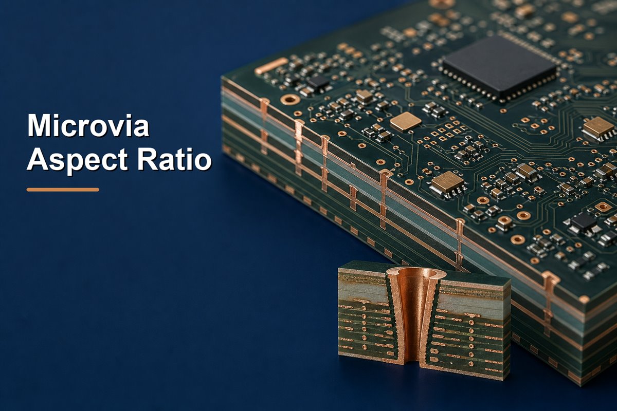
Microvia aspect ratio describes the relationship between the depth of a microvia and its diameter. In its simplest form:
Microvia aspect ratio = microvia depth ÷ microvia diameter
For example, a 75 μm deep microvia with a 100 μm diameter has an aspect ratio of 0.75:1. A 100 μm deep microvia with the same diameter has a ratio of 1:1.
Confirm the fabricator’s conventions before calculating:
- Does depth mean dielectric distance only, or does it include relevant copper?
- Does diameter mean the drilled opening or finished opening?
- Do CAD, fabrication drawings, and CAM use the same values?
IPC-linked definitions commonly use a maximum ratio of 1:1 and total depth of 0.25 mm. This identifies the structure; it does not guarantee that every 1:1 design is easy to produce or reliable.
Calculating early prevents the team from completing BGA escape routing around a hole geometry that cannot be produced with enough margin.
How Do You Calculate Via Aspect Ratio?
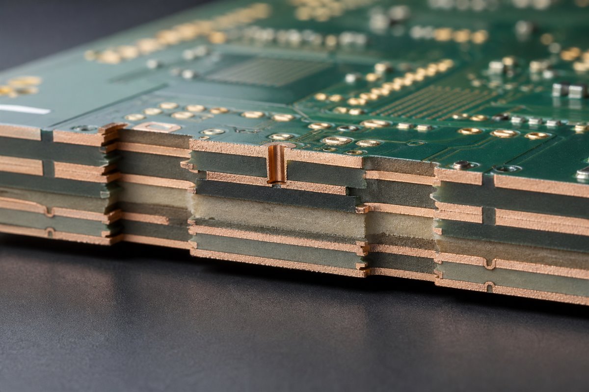
Start with the production stackup, not the nominal finished board thickness. A through-hole via crosses most or all of the board, but a laser microvia normally connects a much shorter layer span. Its depth should therefore be taken from the actual build-up dielectric and land construction for that layer pair.
Use this calculation sequence:
- Identify the microvia start and stop layers.
- Record the actual dielectric thickness between the relevant lands.
- Confirm whether the fabricator includes outer or target copper in the depth calculation.
- Confirm whether the denominator is the drilled opening or finished diameter.
- Divide the confirmed depth by the confirmed diameter.
- Repeat the calculation for every microvia family rather than assuming one value covers the entire board.
Example: an L1–L2 microvia with an 80 μm depth and 100 μm diameter is 0.8:1. A second layer pair with a 100 μm depth and the same diameter is 1:1. Calculate them separately even if their CAD pad stacks look identical.
Record the result beside the drill definition or stackup note so every reviewer uses the same geometry.
What PCB Aspect Ratio Is Suitable for Microvias?
No single production number suits every PCB. Check the ratio against:
- Material and dielectric tolerance.
- Via profile and target-pad preparation.
- Plating, filling, and lamination capability.
- Assembly exposure and reliability requirements.
A 1:1 ratio is widely cited in IPC-linked definitions. Industry guidance often prefers about 0.75:1 or below because a shallower, wider structure gives drilling, plating, and filling more margin. These are design references, not universal guarantees.
Treat the ratio as a decision gate:
- Below the supplier’s established production target: proceed with normal DFM confirmation.
- Near the supplier’s limit: review tolerances, via profile, plating, fill, registration, and reliability evidence.
- Above the supplier’s confirmed limit: increase the diameter, reduce the dielectric depth, or change the HDI construction before release.
Confirm that any published maximum applies to the selected material, copper, quantity, and inspection level. Prototype feasibility is not automatically a production rule.
How Does Microvia Size Change the Result?
For a fixed depth, a smaller diameter increases the ratio and reduces process margin. Use the largest microvia that still completes the required escape routing.
Consider an 80 μm depth:
| Microvia diameter | Calculated ratio | Design implication |
|---|---|---|
| 125 μm | 0.64:1 | Wider geometric margin, if pad and routing space allow |
| 100 μm | 0.80:1 | Requires confirmation against the selected process |
| 80 μm | 1.00:1 | At the commonly cited definition limit and needs close review |
Also confirm:
- Capture and target-pad size.
- Registration tolerance and BGA pitch.
- Via-in-pad treatment and copper filling.
- Component pitch, fanout approach, and affected layer pairs.
EBest Circuit can review manufacturability and assembly interfaces. The customer retains responsibility for component selection, electrical fanout, and the released layout.
How Do You Check Blind Via Aspect Ratio?
First identify whether the feature is a laser microvia or a mechanically drilled blind via. They use different processes and may use different ratio conventions.
For a laser blind microvia, use the controlled depth of its specific build-up layer pair. For a mechanically drilled blind via spanning a thicker section, use the actual controlled drilling depth and the diameter convention stated by the fabricator. Do not calculate either feature from the full board thickness unless it actually passes through that thickness.
Check these items together:
- Via type and drilling method.
- Start and stop layers.
- Nominal and tolerance-controlled depth.
- Drilled and finished diameter definitions.
- Capture and target-pad dimensions.
- Filling, plugging, capping, or planarization requirements.
- Sequential lamination stage.
- Inspection and acceptance method.
This classification prevents quotation errors and late CAM questions about the required drilling process.

When Should You Use a Via Aspect Ratio Calculator?
A calculator quickly flags via families moving toward a process limit. Use it:
- During stackup planning.
- Before BGA fanout is frozen.
- After a dielectric or layer-pair change.
- Before design release.
A calculator cannot approve the design because it does not know the supplier’s actual process or the product’s reliability requirements. Use its result to trigger engineering review, not replace supplier confirmation.
Save the formula convention, source dimensions, layer pair, revision, and supplier response with the result.

Stacked Microvias vs Staggered Microvias
The main trade-off is:
- Stacked microvias: save routing area but add interfaces, filling, planarization, alignment, and sequential processing.
- Staggered microvias: use more area but avoid placing every interface on one vertical load path.
Calculate every microvia level separately. Do not divide the full stack height by one hole diameter. Also review the interfaces, lamination count, filling, planarization, and required thermal-stress evidence.
Use stacked construction only when its density benefit is necessary and the fabrication and qualification plan supports it. Otherwise, staggered structures may offer a more controllable production path.
A Calculation Example Before PCB Release
Consider a compact control board with a fine-pitch BGA. The preliminary layout uses 80 μm laser holes through a 100 μm build-up depth. The calculated ratio is 1.25:1, which is above the commonly cited 1:1 microvia definition boundary and outside the comfortable range described by much industry guidance.
If routing is completed first, a later stackup change may affect impedance, BGA escape, cost, and delivery.
The engineering team evaluates three options:
- Increase the laser diameter where the BGA pad and routing space allow.
- Reduce the build-up dielectric depth using an approved manufacturable stackup.
- Change the layer-transition strategy, including selective use of staggered structures.
The team selects a 100 μm hole with an 80 μm depth, producing 0.8:1. Before freezing the layout, it sends the revised stackup, drill table, pad geometry, fill requirement, impedance information, and reliability expectations to the fabricator.
This is an illustrative scenario. The key sequence is:
- Calculate the ratio.
- Compare it with the supplier’s process window.
- Revise before routing is frozen.
- Document supplier confirmation.
What Should You Send for DFM Review?
A manufacturer cannot confirm feasibility from the ratio alone. The review package must show the complete PCB construction and acceptance needs.
Prepare these files and decisions:
- Gerber or ODB++ data and NC drill files.
- Controlled stackup with layer numbers and dielectric thicknesses.
- Drill table identifying every via family and start/stop layer.
- Drilled versus finished diameter convention.
- Copper weights and plating requirements.
- Pad stacks, target lands, and critical BGA footprints.
- Via-in-pad filling, capping, and planarization requirements.
- Impedance requirements and test-coupon needs.
- Material requirements and acceptable alternatives.
- Prototype and production quantities.
- Inspection, thermal-stress, electrical-test, and acceptance requirements.
- BOM and placement files if PCBA review is also required.
EBest Circuit (Best Technology) can use the released information to review PCB manufacturability, align fabrication and PCBA requirements, and coordinate agreed inspection or testing. If a value is still open, mark it as requiring supplier confirmation rather than allowing CAM assumptions to become an uncontrolled design decision.
For an HDI DFM review or PCB quotation, send the available project files and requirements to sales@bestpcbs.com.
FAQs About Via Aspect Ratio
Is 1:1 always a safe microvia aspect ratio?
No. It is commonly cited as an IPC-linked definition limit, but actual production suitability depends on materials, geometry, process controls, assembly exposure, and reliability requirements. Many design guides prefer additional margin below 1:1.
Should microvia depth include copper thickness?
Use the fabricator’s documented convention. Some calculations focus on dielectric depth, while others include relevant foil or land construction. Record the convention beside the result so every reviewer uses the same inputs.
Can one aspect ratio cover all microvias on a PCB?
Only if every microvia family has the same confirmed depth and diameter convention. Different layer pairs or stackup regions should be calculated separately.
Does a lower ratio guarantee microvia reliability?
No. A lower ratio generally improves geometric process margin, but material properties, target-pad preparation, copper deposition, fill quality, registration, lamination, assembly cycles, and qualification testing also matter.
When should the fabricator confirm the ratio?
Before the stackup and BGA fanout are frozen, and again after any change to dielectric thickness, hole size, copper construction, via type, or reliability requirement.
Need help checking your microvia aspect ratio before PCB release? Send your stackup, drill information, and available project files to sales@bestpcbs.com for DFM review and quotation support.