VCC vs VDD vs VSS are common labels for IC power-supply pins, but the names do not define a fixed voltage. VCC and VDD usually refer to an upper supply rail, while VSS usually refers to a lower rail or voltage reference. Depending on the device, VCC or VDD may be 5 V, 3.3 V, 1.8 V, or another voltage, while VSS may be 0 V or a negative rail.
The labels help you understand the likely role of a power pin, but the actual connection must come from the datasheet. Before assigning a rail, check the pin function, recommended voltage range, reference node, power domain, and sequencing requirements.
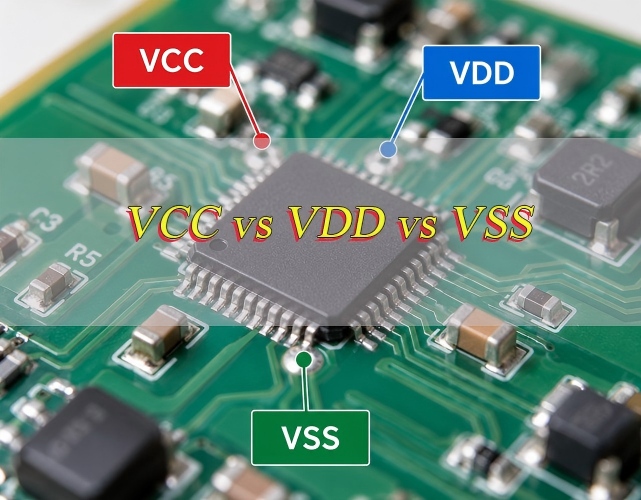
What Do VCC, VDD, and VSS Mean?
VCC, VDD, VSS, and VEE originated from transistor terminology, but modern ICs use them mainly as supply-rail names. Their historical meaning helps explain the letters, but it does not determine the voltage a device requires.
- VCC — collector supply: historically associated with bipolar-transistor collectors and now commonly used for an upper supply rail.
- VDD — drain supply: derived from MOS transistor drain notation and commonly used for an upper CMOS supply.
- VSS — source supply: derived from MOS source notation and usually used for the lower rail or reference.
- VEE — emitter supply: historically associated with bipolar-transistor emitters and often used for a lower or negative rail.
A modern IC may use VCC even though it contains CMOS circuitry, while another device may use several VDD rails for different internal blocks. Names such as VDDIO, VDDCORE, AVDD, and VDDPLL often tell you more about the required connection than VCC or VDD alone.
The complete pin name and its electrical specification matter more than the historical meaning of CC, DD, or SS.
VCC vs VDD vs VSS: What Is the Practical Difference?
For PCB design, the most useful difference is the role and position of each supply rail. VCC and VDD usually identify upper supplies, while VSS usually identifies a lower supply or reference.
| Aspect | VCC | VDD | VSS |
|---|---|---|---|
| Usual role | Upper supply | Upper supply | Lower supply or reference |
| Common connection | Positive board rail | Positive board rail | 0 V return |
| Typical use | Logic, I/O, general supply | Core, I/O, analog, general supply | Ground, return, or negative rail |
| Main check | Voltage and current | Voltage, domain, sequencing | Relationship to GND |
On a simple 3.3 V board, a sensor with a VCC pin and a microcontroller with a VDD pin may both connect to +3V3. That is acceptable because both devices support the same voltage, not because VCC and VDD are automatically interchangeable.
The difference becomes more important in multi-rail ICs. A processor may use VDDCORE at 1.0 V while VDDIO operates at 3.3 V. An analog rail may use the same nominal voltage as a digital rail but still require separate filtering or decoupling.
For VCC vs VDD vs VSS, use the labels to identify the general rail role, then check the device specification before deciding how the pins should be connected.
Are VCC and VDD the Same?
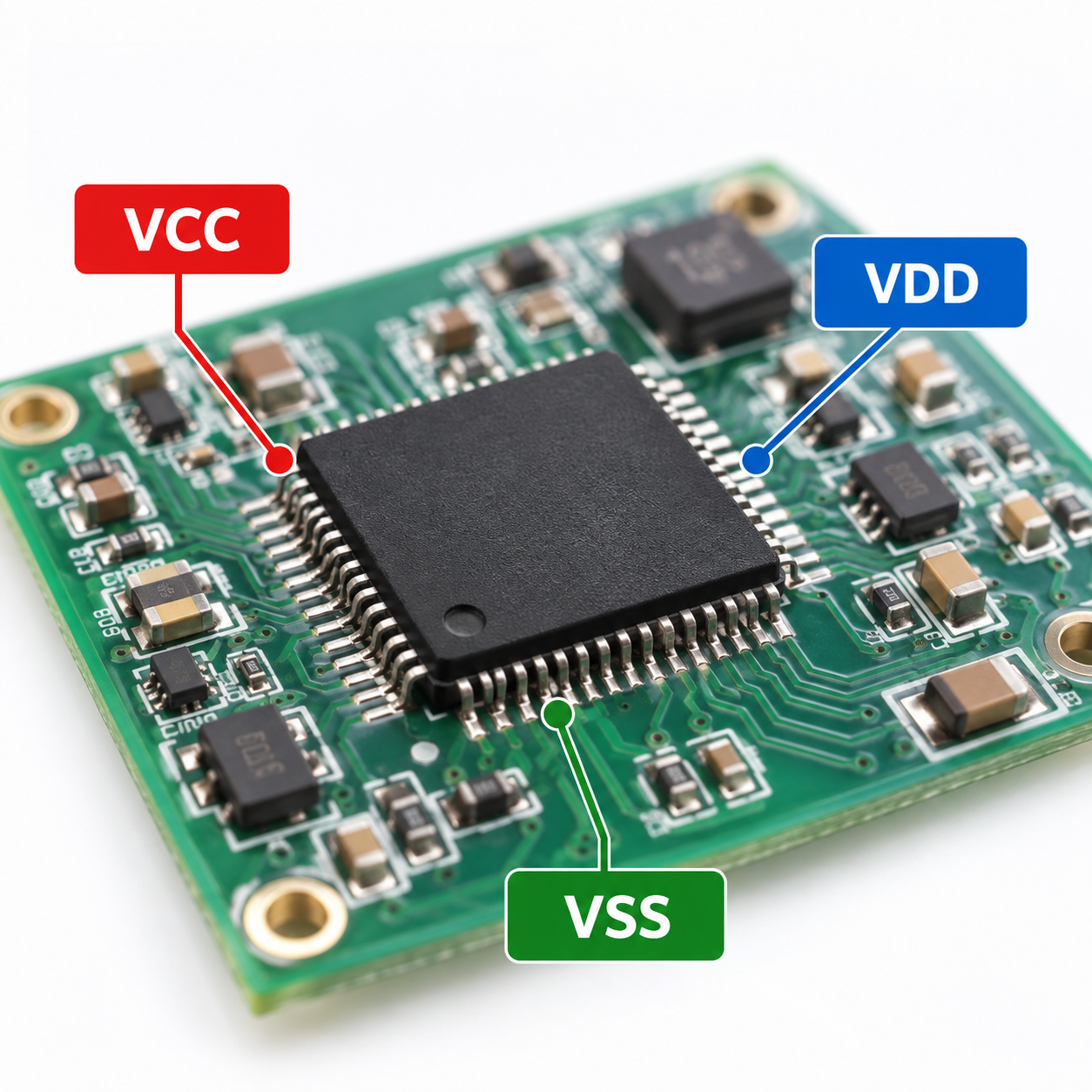
VCC and VDD can serve the same general purpose, but they are not always electrically equivalent.
If a 3.3 V sensor uses VCC and a 3.3 V microcontroller uses VDD, both may connect to the same +3V3 rail when their datasheets allow it. A different device, however, may separate VDDCORE, VDDIO, and AVDD because each domain has its own voltage, noise, or startup requirements.
Before connecting VCC and VDD to the same source, verify:
- Their allowed voltage ranges overlap.
- The regulator can supply the combined current.
- Neither rail requires separate filtering.
- Their startup and shutdown requirements are compatible.
- One powered domain cannot back-power another through signal pins.
Even when two rails use the same nominal voltage, the reference design may still require separate ferrites, local capacitors, or controlled sequencing.
Treat VCC and VDD as interchangeable only when the datasheet shows that their electrical requirements are compatible.
Is VSS the Same as Ground?
VSS often connects to ground, but it is not always the same electrical node.
In many single-supply digital circuits, VSS connects directly to the 0 V ground plane. This is common in microcontrollers and logic ICs, which is why VSS is often treated as ground in simple schematics.
A split-supply circuit is different. For example:
- VDD = +3.3 V
- GND = 0 V
- VSS = -3.3 V
In this arrangement, VSS is a negative supply rather than ground.
The same caution applies to AGND, DGND, chassis ground, exposed pads, and other return pins. They may ultimately share a reference, but the datasheet can specify where and how those connections should be made.
Connect VSS to ground only when the device documentation defines VSS as the 0 V reference.
What Voltage Should VCC, VDD, and VSS Be?
There is no standard voltage for VCC, VDD, or VSS. The correct value depends on the exact component and power domain.
Common arrangements include:
- 5 V logic: VCC = 5 V, VSS or GND = 0 V
- 3.3 V CMOS: VDD = 3.3 V, VSS = 0 V
- Low-voltage core: VDDCORE = 1.0 V or 1.2 V
- Split-supply analog circuit: VDD = +3.3 V, VSS = -3.3 V
These are examples, not default values.
For the actual operating voltage, check the recommended operating conditions for the exact part number and package. Do not use the absolute maximum rating as a normal design target; that table describes stress limits rather than the preferred operating point.
Also check how the voltage is referenced. If a datasheet specifies VDD relative to VSS, the voltage difference between those rails matters. For example, VDD = +2.5 V and VSS = -0.8 V produces a 3.3 V difference across the device.
The pin label tells you the rail’s likely role; the datasheet tells you the voltage.
Why Do ICs Use Multiple Power Rails?
Modern ICs often contain digital logic, analog circuits, I/O banks, memories, PLLs, and other blocks with different voltage or noise requirements. Separate power names make those domains easier to identify and control.
Common examples include:
- AVDD / AVSS: analog supply and return
- DVDD / DVSS: digital supply and return
- VDDIO / VCCIO: I/O supply
- VDDCORE / VCCINT: internal core supply
- VDDPLL / AVSSPLL: PLL or clock supply
- VBAT: backup or retention supply
Some rails operate at different voltages. Others use the same nominal voltage but require different filters or local decoupling because their noise requirements are different.
Large IC packages may also provide several pins with the same supply name. These pins can distribute current, reduce connection impedance, or feed different sections of the die.
Do not leave a repeated supply pin unconnected simply because another pin has the same name. Follow the connection requirements for the exact device and package.
How Do You Check VCC vs VDD vs VSS in a Datasheet?
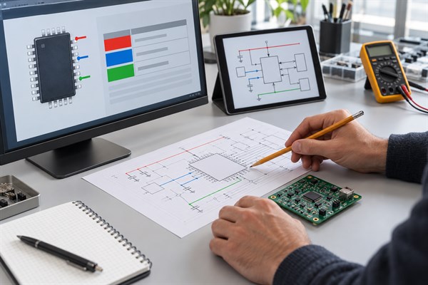
The pin name is only the starting point. To determine the correct VCC vs VDD vs VSS connection, check the datasheet in a consistent order.
1. Check the pin description.
Confirm whether the pin is a supply input, return, reference, regulator output, or exposed pad.
2. Check the recommended operating conditions.
Find the normal voltage range and identify the reference node used for that specification.
3. Check the power or block diagram.
Determine whether the rail supplies the core, I/O, analog circuitry, memory, PLL, or another domain.
4. Check the typical application circuit.
See whether the manufacturer joins the rail to another supply, filters it separately, or places dedicated decoupling nearby.
5. Check power sequencing.
Some devices require one rail to rise before another, while others limit external signals until a supply is stable.
Each section answers a different question. A pin table may tell you that VDDIO is a supply input, while the electrical table gives its permitted voltage range. The application circuit then shows how that rail should be connected and decoupled.
This process also tells you whether VCC and VDD can share one regulator. Similar names are not enough; the voltage, current, noise, sequencing, and back-power requirements must all be compatible.
Can VCC and VDD Share the Same Power Rail?
Yes, but only when their electrical requirements allow it. The same rule applies whether the rails belong to one IC or to different components.
| Factor | Share One Rail When | Keep Them Separate When |
|---|---|---|
| Voltage | Both support the same voltage range | Their operating ranges differ |
| Function | Both can use the same source | Core, analog, RF, or I/O domains have separate requirements |
| Noise | One source and normal decoupling are sufficient | Filtering or isolation is required |
| Startup | The rails may rise together | A defined sequence is required |
| Back-powering | Signals cannot feed an unpowered domain | Interface pins may drive a rail that is off |
A shared +3V3 rail, for example, is reasonable when both devices support that voltage, the regulator can supply the required current, and there are no conflicting noise or sequencing requirements.
A shared supply should be justified by compatible electrical requirements, not by similar-looking pin names.
What Happens If VCC, VDD, or VSS Is Wired Incorrectly?
Incorrect supply wiring can cause anything from unstable startup to permanent IC damage. The symptom depends on the type of error.
- Voltage too high: may overstress internal junctions or gate oxides and cause overheating or failure.
- Voltage too low: may cause resets, failed startup, incorrect logic levels, or unstable analog performance.
- VCC or VDD reversed with VSS: can force current through internal structures and quickly damage the IC.
- Required power pin left open: may disable part of the device or cause intermittent operation.
- Separate power domains shorted together: can create regulator contention, overvoltage, or unwanted noise coupling.
- Signals applied before the supply is active: may back-power an unpowered domain through input protection paths.
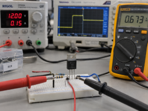
When troubleshooting, measure the voltage at the actual IC power pins, not only at the regulator output. A regulator may show the correct voltage while the device receives the wrong level because of an open trace, voltage drop, wrong net assignment, or missing return connection.
FAQs About VCC vs VDD vs VSS
Q1: Are VCC and VDD the same?
A1: They can perform the same general function, but they are not automatically interchangeable. They may share a rail when their voltage range, filtering, sequencing, and other electrical requirements are compatible.
Q2: Is VSS always ground?
A2: No. VSS commonly connects to 0 V in single-supply circuits, but it may be a negative rail in a split-supply design.
Q3: What is the difference between VDD and VIN?
A3: VDD usually powers an internal device domain, while VIN usually refers to an incoming supply or functional voltage input.
Q4: What is the difference between VSS and VEE?
A4: VSS comes from MOS source terminology, while VEE comes from bipolar emitter terminology. Both are commonly used for lower supply rails, but their actual voltage depends on the circuit.
Q5: Can one circuit use both VCC and VDD?
A5: Yes. Different components may use different naming conventions, and one IC may include several independently named supply domains.
Q6: Do all VDD and VSS pins need to be connected?
A6: Usually yes when the datasheet identifies them as power pins. Multiple pins may distribute current or supply different sections of the die, so follow the connection requirements for the exact device and package.
If you are unsure whether your VCC, VDD, and VSS rails are assigned correctly, it is better to catch the issue before PCB fabrication or assembly. EBest Circuit can review your schematic, BOM, component datasheets, intended rail voltages, and power-sequencing requirements to help identify unclear or potentially incorrect power-net connections.
Would you like to get a PCB or PCBA quote with design review support? Send your project files and requirements to sales@bestpcbs.com.