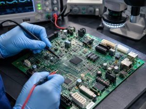
USB hub PCB board is the core circuit board inside a USB hub device. It connects one upstream USB port to multiple downstream USB ports, allowing computers, industrial controllers, embedded systems, docking stations, test equipment, and smart devices to connect several USB peripherals through one board.
For engineers and buyers, a USB hub PCB board is not only a connector board. It involves USB data routing, power distribution layout, ESD protection layout, controller IC footprint and placement review, connector reliability, SMT assembly, and functional testing. EBest Circuit (Best Technology) supports custom USB hub PCB manufacturing, FR4 PCB fabrication, component sourcing based on the approved BOM, PCBA assembly, DFM review, and testing support. If you are developing a USB hub PCB board, send your Gerber data, ODB++ files, fabrication drawing, approved BOM, assembly notes, impedance requirements, or technical specifications to sales@bestpcbs.com for engineering review before production.
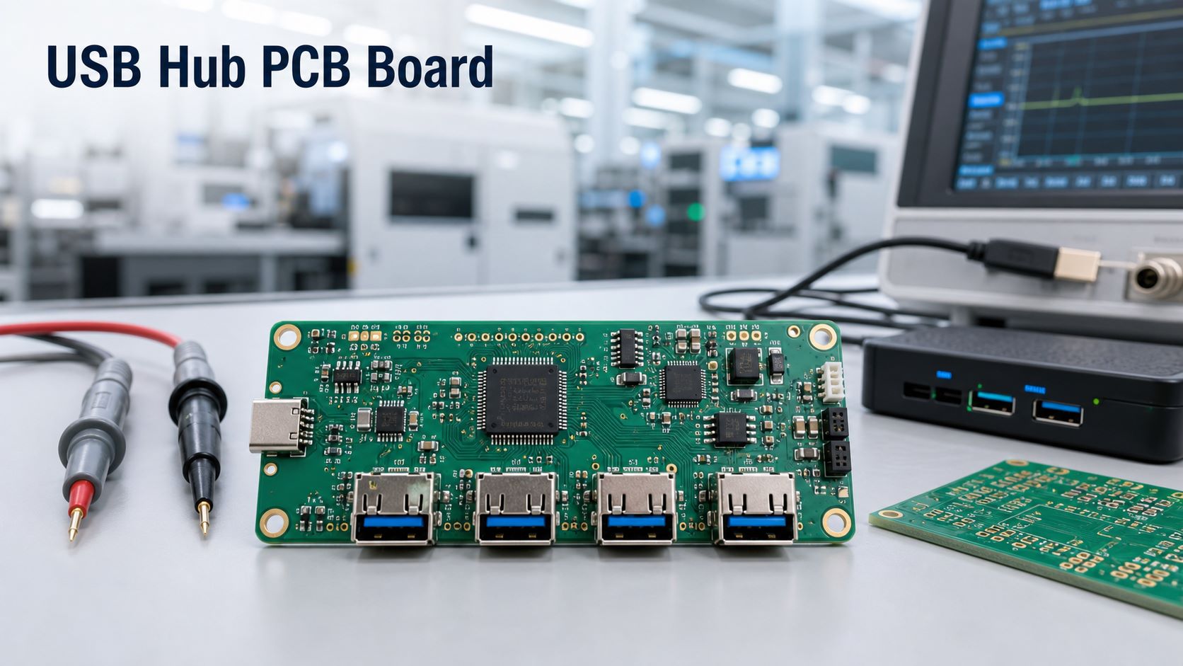
What Is a USB Hub PCB Board?
A USB hub PCB board is a printed circuit board that expands one USB connection into multiple USB ports. It usually contains a USB hub controller IC, upstream connector, downstream connectors, power management circuit, ESD protection devices, and supporting passive components.
The USB hub controller IC, power circuit, and protection circuit are usually defined by the customer’s engineering team. EBest Circuit focuses on PCB layout manufacturability, PCB fabrication, component sourcing based on the approved BOM, PCB SMT assembly, and testing support.
Common USB hub PCB board applications include:
| Application | Typical Need |
|---|---|
| Consumer USB hub | Multiple USB-A ports |
| Industrial controller | Stable embedded USB expansion |
| Docking station | Data and power integration |
| Test equipment | Reliable peripheral connection |
| Medical device | Stable signal and documentation |
| Smart terminal | Compact custom board shape |
| Embedded system | OEM board integration |
The key point is that a USB hub board must handle both data and power correctly. Poor routing, weak grounding, missing ESD placement review, or unstable power distribution layout can cause connection failures, unstable device detection, or signal loss.
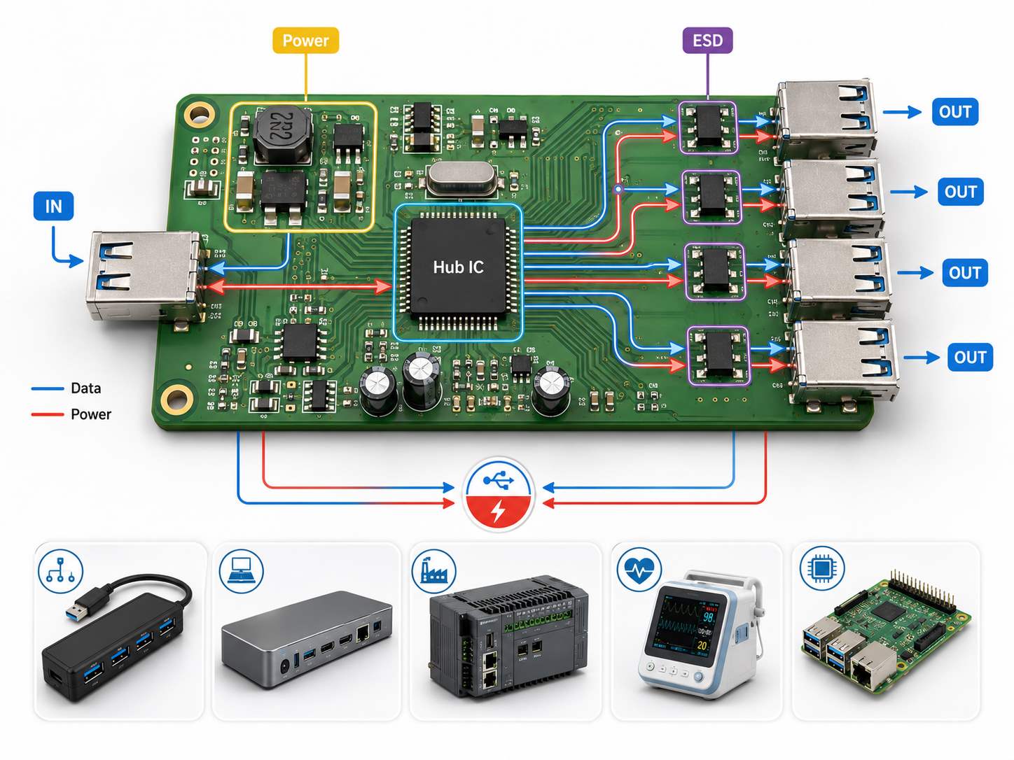
USB Hub PCB Board Structure and Key Components
A USB hub PCB board usually includes several important functional blocks.
| Component | Function |
|---|---|
| USB hub controller IC | Manages upstream and downstream USB communication |
| Upstream port | Connects to host computer or main system |
| Downstream ports | Connect to USB devices |
| Crystal or oscillator | Provides clock reference |
| ESD protection | Protects USB lines from static discharge |
| Power switch / current limit IC | Controls downstream port power |
| Voltage regulator | Provides stable voltage to ICs |
| LED indicators | Show power or port status |
| Connectors | USB-A, USB-B, Micro USB, USB-C, board-to-board connector |
| PCB stackup | Supports routing, grounding, and impedance control |
For a custom USB hub PCB board, the component layout must consider connector direction, enclosure fit, cable insertion force, thermal behavior, test access, and SMT PCB assembly process.
A good manufacturer should not only check whether the board can be fabricated. The PCB and PCBA team should also review connector footprint, solder joint strength, copper clearance, ESD placement, and final inspection requirements.
FR4 USB Hub PCB Board Material and Layer Options
Most USB hub PCB boards use FR4 material because it offers a practical balance of cost, mechanical strength, dielectric performance, and manufacturing availability.
Common layer choices include:
| PCB Type | Suitable For |
|---|---|
| 2 layer FR4 PCB | Simple USB 2.0 hub boards |
| 4 layer FR4 PCB | Better grounding, impedance, and power distribution |
| 6 layer PCB | High-density or more complex USB 3.0 / Type-C designs |
For simple USB 2.0 boards, 2 layers may be enough if routing is not crowded and power distribution is simple. For USB 3.0, compact products, multiple ports, or EMI-sensitive applications, 4 layers are often more practical because they allow better ground reference and cleaner routing.
Important FR4 USB hub PCB board specifications include:
- Board thickness
- Tg value
- Copper thickness
- Surface finish
- Solder mask color
- Connector footprint
- Impedance requirement
- Via structure
- Panelization requirement
- Assembly and test plan
If the product will be used in industrial equipment, enclosed devices, or higher-temperature environments, Tg150 or Tg170 material may be preferred over standard Tg130 FR4.
USB Hub Circuit Board Layout Checks for Data and Power Paths
From a PCB layout and manufacturing view, a USB hub circuit board should keep two paths clear and reliable: the USB data path and the power distribution path.
Data path
For the data path, the customer’s schematic and selected USB hub controller define the circuit. During PCB layout and manufacturing review, the focus is whether the USB signal paths can be routed cleanly and manufactured reliably.
Key layout checks include:
- USB 2.0 D+ / D- differential pair routing
- USB 3.0 SuperSpeed TX/RX differential pair routing
- Short and clean routing between connector and controller IC
- Continuous reference plane under USB signal lines
- Proper spacing from noisy power areas
- ESD device placement close to connectors
- Avoiding unnecessary vias or stubs on high-speed lines
Power path
For the power path, the customer usually defines the power circuit, protection components, and current requirements. EBest Circuit reviews the PCB layout and manufacturing details that affect power stability and assembly reliability.
Important checks include:
- Copper width for USB port power
- Ground return path
- Thermal relief around power components
- Footprint and placement of customer-specified protection devices
- Connector current rating and soldering reliability
- Decoupling capacitor placement according to the customer’s design files
- Clearance around high-current areas
A stable USB hub PCB board should not treat power routing as an afterthought. If the downstream ports draw current, copper width, copper thickness, thermal relief, and connector current rating should be checked before production.
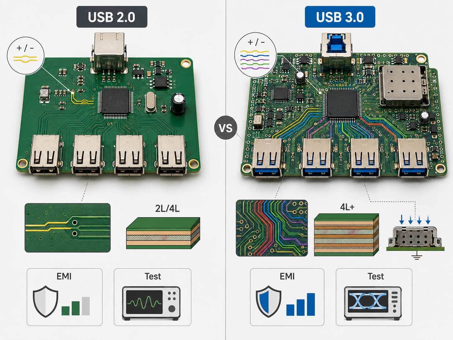
USB 2.0 and USB 3.0 Hub Board Manufacturing Differences
USB 2.0 and USB 3.0 hub boards have different PCB manufacturing concerns.
| Item | USB 2.0 Hub Board | USB 3.0 Hub Board |
|---|---|---|
| Signal speed | Lower | Higher |
| Routing | D+ / D- differential pair | Multiple high-speed differential pairs |
| Layer count | 2L or 4L common | 4L or more often preferred |
| Impedance | Important | More critical |
| EMI control | Moderate | More demanding |
| Connector routing | Simpler | More complex |
| Testing | Basic functional test | Signal and functional test more important |
For USB 2.0, routing and grounding still matter, but the board is usually more forgiving. For USB 3.0, impedance control, differential pair matching, reference planes, connector breakout, via transitions, and shielding become more important.
From a manufacturing point of view, USB 3.0 hub boards often need closer review of stackup, trace width, spacing, solder mask, and test requirements.
4-Port USB Hub Board Layout and Assembly Checks
A 4-port USB hub board is one of the most common USB hub PCB formats. It usually has one upstream port and four downstream ports, but the actual layout can vary depending on enclosure, cable direction, and product application.
Important layout and assembly checks include:
- USB connector alignment
- Downstream port spacing
- Upstream connector position
- Controller IC placement according to customer design files
- Short and balanced differential pair routing
- ESD protection close to connectors
- Customer-specified power switch and fuse placement
- Sufficient copper for port power
- Ground continuity
- SMT solderability of connectors
- Mechanical strength under insertion force
- Test point access
Connectors are one of the most important reliability points. A USB hub PCB board may pass electrical testing, but if connector solder joints are weak or mechanical stress is not considered, field reliability can still be poor.
For PCBA assembly, connector type, solder paste volume, reflow profile, AOI inspection, and manual inspection should be reviewed before production.
USB Hub PCB Board Signal Integrity and Impedance Control
USB signals rely on differential pair routing. This makes signal integrity important, especially for USB 3.0 and compact hub boards.
Key PCB layout points include:
- Differential pair width and spacing
- Controlled impedance
- Length matching
- Continuous reference plane
- Minimal stubs
- Careful via transitions
- Good connector breakout
- ESD component placement
- Avoiding splits under high-speed lines
For many USB designs, the differential impedance target is around 90 ohms, but the exact requirement should follow the USB controller IC reference design and customer specification.
Impedance control depends on:
| Factor | Why It Matters |
|---|---|
| PCB stackup | Defines dielectric spacing and reference plane |
| Copper thickness | Affects final trace width |
| Trace width/spacing | Controls impedance value |
| Solder mask | Can affect impedance slightly |
| Material | Affects dielectric constant |
| Manufacturing tolerance | Affects repeatability |
EBest Circuit can review stackup, impedance notes, and manufacturing feasibility before production. If the customer requires impedance reporting, the test coupon and report should be planned before fabrication.
USB Hub PCBA Testing and Quality Control
USB hub PCBA testing should confirm that the assembled board works as a real product, not only as a bare PCB.
Common quality checks include:
| Test / Check | Purpose |
|---|---|
| Visual inspection | Checks solder joints, connectors, polarity, and cleanliness |
| AOI | Detects SMT placement and soldering defects |
| X-ray if needed | Checks hidden solder joints |
| Electrical test | Confirms bare PCB connectivity |
| Functional test | Confirms USB hub operation |
| Port detection test | Checks each downstream USB port |
| Power test | Checks current and voltage stability |
| ESD-related review | Confirms protection device placement |
| Cleaning inspection | Reduces contamination risk |
| Packing control | Protects connectors and assembled boards |
For USB hub PCB assembly, functional testing is especially important. Each port should be checked, because a board can look acceptable after SMT but still have data, power, or connector-related issues.
If the product will be installed inside industrial equipment, medical devices, smart terminals, or custom enclosures, the inspection plan should also match the final application.
USB Hub PCB Board Manufacturing Case Study
A European customer developed a custom USB hub PCB board for an embedded control device used inside industrial equipment. The board needed compact size, stable USB connection, reliable via filling, and good assembly quality.
Project snapshot
- Customer: Europe
- Application: Embedded USB expansion board for industrial equipment
- Board type: 4L FR4 PCB
- Material: FR4 Tg170
- Finished thickness: 0.8mm +/-0.1mm
- Copper thickness: 1oz inner and outer copper
- Solder mask / silkscreen: Green solder mask, no silkscreen
- Surface finish: ENIG, Au 1u”
- Special process: Copper paste filling for vias <=0.6mm
- Main focus: Thin 4-layer structure, via filling reliability, solderability, and assembly readiness
Main challenge
This USB hub PCB board was thinner than a standard 1.6mm board, so the stackup and manufacturing tolerance needed to be reviewed carefully. The customer also required copper paste filling for all vias smaller than or equal to 0.6mm. This requirement was important for reliability, surface flatness, and downstream assembly control.
EBest Circuit solution
- Reviewed the 4L FR4 Tg170 stackup before production
- Checked whether 0.8mm +/-0.1mm thickness was feasible with the required copper structure
- Confirmed 1oz inner and outer copper for manufacturing stability
- Controlled via copper paste filling for vias <=0.6mm
- Checked ENIG Au 1u” for solderability and connector contact reliability
- Reviewed the no-silkscreen requirement to avoid unwanted marking
- Prepared the board for reliable SMT assembly and inspection
Customer value
For the customer, this was not just a USB hub PCB board order. The value was early manufacturing review: board thickness, Tg170 material, via filling, ENIG finish, and assembly requirements were checked before production. This helped reduce avoidable risks and made the board more suitable for an embedded industrial USB hub application.
How to Choose an OEM USB Hub Board Manufacturer
When choosing an OEM USB hub board manufacturer, do not only compare the bare PCB price. A USB hub project usually involves PCB fabrication, component sourcing based on an approved BOM, SMT assembly, connectors, power testing, and functional validation.
A practical OEM supplier should support:
- FR4 PCB manufacturing
- 2L, 4L, or multilayer PCB production
- Controlled impedance review
- USB connector assembly
- ESD and power protection component placement based on customer files
- Component sourcing based on approved BOM
- SMT assembly
- Functional testing
- DFM review before production
- Packaging protection for connectors
EBest Circuit supports one-stop PCB and PCBA service, including PCB fabrication, component sourcing, SMT assembly, DFM review, BOM support, testing coordination, and small-batch production. For USB hub PCB board projects, our engineering team can review manufacturability, stackup, connector assembly, surface finish, via process, and testing needs before production starts.
FAQs about USB Hub PCB Board
1. What is a USB hub PCB board?
A USB hub PCB board is the circuit board inside a USB hub. It connects one upstream USB port to multiple downstream USB ports through a USB hub controller IC and supporting power, protection, and connector circuits.
2. Is FR4 suitable for a USB hub PCB board?
Yes. FR4 is commonly used for USB hub PCB boards because it offers good mechanical strength, cost control, and stable manufacturing. For industrial or higher-temperature applications, Tg150 or Tg170 FR4 may be preferred.
3. Does a USB hub PCB board need controlled impedance?
Many USB hub boards need impedance review, especially USB 3.0 or compact high-speed designs. Differential pair routing, stackup, trace width, spacing, and reference planes should be checked before production.
4. What is the difference between USB 2.0 and USB 3.0 hub boards?
USB 2.0 hub boards are usually simpler and may use 2 or 4 layers. USB 3.0 hub boards require more careful high-speed routing, impedance control, connector breakout, grounding, and testing.
5. Can EBest Circuit manufacture and assemble USB hub PCB boards?
Yes. EBest Circuit supports custom USB hub PCB manufacturing, FR4 PCB fabrication, component sourcing based on the approved BOM, SMT assembly, DFM review, and testing coordination for prototype and small-batch production.
Overall, if you are developing a custom USB hub PCB board, OEM USB hub board, USB 2.0 hub board, USB 3.0 hub board, or USB hub PCBA project, send your Gerber data, ODB++ files, fabrication drawing, approved BOM, assembly notes, impedance requirements, or technical specifications to sales@bestpcbs.com. EBest Circuit’s engineering team can help review the PCB layout manufacturability, fabrication process, SMT assembly, and testing path before production.