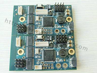
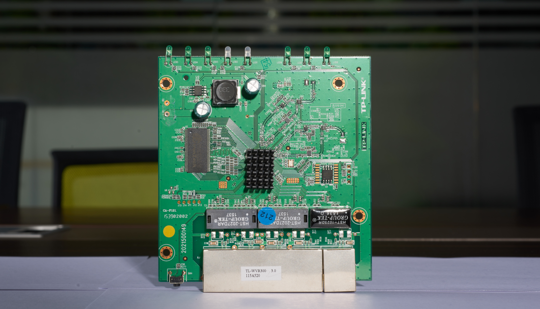
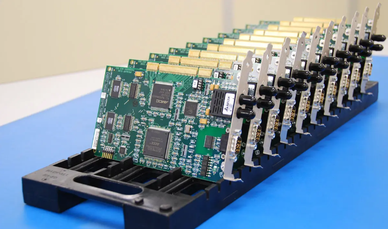
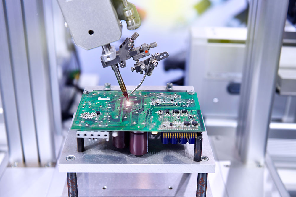
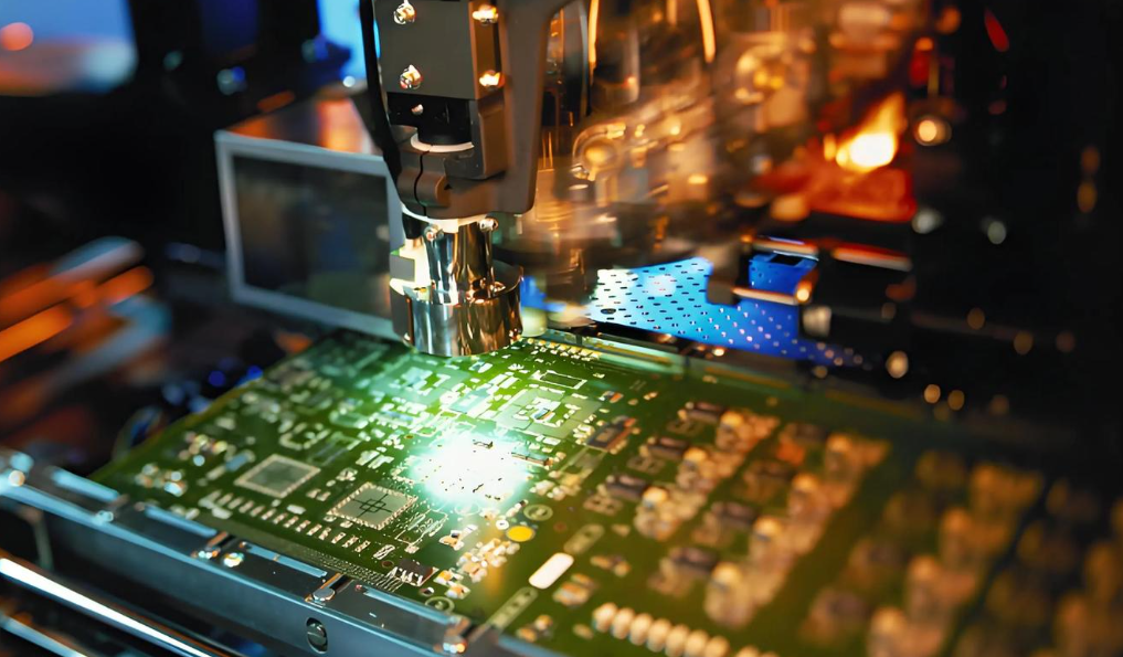
Our surface mount pcb assembly services mounts electronic components directly onto PCB pads using solder paste printing, automated placement, and ref low soldering. At EBest Circuit, we combine assembly-focused design review, component sourcing, SMT production, and inspection for prototypes and production orders. Our documented capabilities include 01005 SMD components and BGA packages down to 0.25 mm pitch, subject to review of the actual package, board layout, and inspection requirements. We can supply SMT-only assemblies or combine SMT with through-hole assembly, programming, and functional testing to match your product requirements.

Key Takeaways
- SMT attaches components to surface pads; a repeatable build depends on paste printing, placement, and ref low working together.
- Our surface mount PCB assembly services cover SMT, mixed SMT/THT builds, consigned parts, partial turnkey, and full turnkey production.
- Documented capabilities include 01005 components and 0.25 mm BGA pitch; the complete board still needs package-specific manufacturing review.
- SPI measures printed paste, AOI checks visible assembly features, and X-ray examines hidden joints. Functional testing checks the defined circuit behavior.
- A SAC305 process may use a peak around 235–245°C, but the selected paste specification and measured board profile determine the actual process.
- Stencil design, component availability, assembly sides, hidden-joint inspection, and test fixtures affect cost and scheduling.
What Does Our Surface Mount PCB Assembly Service Include?
We provide component preparation, stencil fabrication, solder paste printing, SMT placement, ref low, and inspection, with PCB fabrication, sourcing, and testing available within the agreed project scope. You can assign the complete build to us or supply selected components yourself.
Our PCB assembly service supports the following production requirements:
| Assembly Item | Our Supported Scope |
|---|---|
| Small SMD components | Down to 01005; footprint, stencil, handling, and inspection reviewed together |
| Fine-pitch BGA | Down to 0.25 mm pitch; package-specific DFM and inspection planning |
| Assembly types | SMT, through-hole, mixed SMT/THT |
| Package families | Chip resistors, capacitors, diodes, transistors, SOIC, QFP, QFN, BGA |
| Component presentation | Reels, cut tape, tubes, trays, loose parts with handling review |
| Supply models | Consignment, partial turnkey, full turnkey |
| Inspection and testing | 3D SPI, AOI, X-ray, functional testing to the agreed test plan |
A minimum package size is not a blanket guarantee for every layout. For example, placing a 01005 passive next to a tall connector may require a different nozzle-access and inspection arrangement from placing the same passive in an open area. We review the assembled board rather than accepting a project from its smallest component alone.
Which Surface Mount PCB Components Can We Assemble?
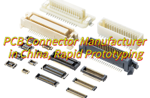
We assemble chip passives, discrete semiconductors, leaded ICs, and leadless or area-array packages such as QFN and BGA. Each family creates different requirements for paste deposition, placement, and joint inspection.
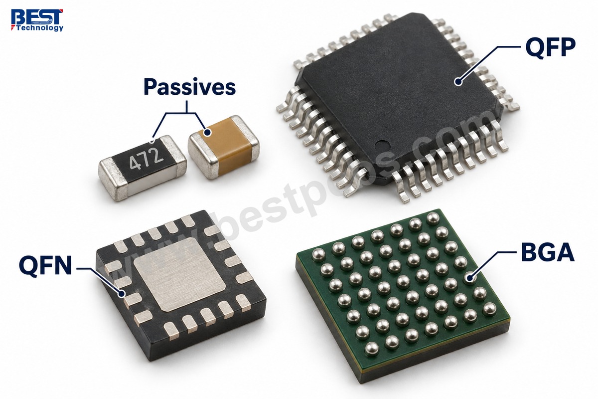
- Chip resistors and capacitors: pad symmetry, paste balance, and heating balance help prevent tombstoning and skew.
- SOIC and QFP: lead coplanarity, fine-pitch paste separation, and placement alignment affect bridging and open joints.
- QFN: the exposed thermal pad and peripheral lands need a package-specific stencil strategy. Excess paste under the center pad can lift the package or disturb perimeter joints.
- BGA: ball pitch, land geometry, board warpage, and ref low behavior determine the process window. Hidden joints require an inspection method beyond ordinary top-side AOI.
We use the exact manufacturer package drawing and approved component part number when checking footprints. Two ICs with the same pin count do not necessarily share the same body dimensions or land pattern.
What Is the Surface Mount Assembly Process?
The surface mount assembly process moves from data and material checks to paste printing, inspection, placement, ref low, and post-solder verification. Finding a printing problem before placement avoids sending the same defect through the rest of the line.
- Review the assembly data. Match the BOM, footprints, placement coordinates, polarity marks, and assembly drawing.
- Prepare components and boards. Verify part identity, packaging condition, and any moisture-sensitive handling requirements.
- Print solder paste. Align the stencil to the PCB and transfer paste through its apertures.
- Inspect the printed deposits. Use SPI to evaluate paste volume, height, area, and positional variation against the process criteria.
- Place the components. Load feeders, verify package orientation, and place parts at the programmed coordinates.
- Reflow the assembly. Heat and cool the board using a profile verified for the actual assembly.
- Inspect and test. Apply AOI, specified X-ray inspection, and the agreed electrical or functional tests.
For double-sided SMT, we plan the assembly sequence around component mass, package restrictions, and exposure to a second ref low cycle. Through-hole parts are added using the selected insertion and soldering process when the board is a mixed assembly.
Which Surface Mount PCB Design Checks Matter Before Production?
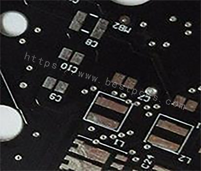
The essential surface mount PCB design checks are footprint accuracy, solder-mask geometry, stencil access, placement clearance, fiducials, and panel support. These features directly affect whether the line can print, place, and inspect the board consistently.
In our PCB design review, a QFN thermal pad receives different attention from a gull-wing QFP. We check the QFN exposed-pad aperture pattern and any via-in-pad construction against the package guidance; for a QFP, we check lead pitch, pad geometry, and paste separation. Open vias in a soldering area can draw solder away from the intended joint.
We also check whether the panel provides reliable conveyor support and whether tooling or board edges interfere with components. Fiducials must remain visible to the placement system. We do not apply one arbitrary rail width, component clearance, or stencil thickness to every product; these dimensions are selected for the actual board and equipment setup.
How Do We Control Solder Paste Printing?
We control solder paste printing by matching the paste and stencil to the package mix, maintaining alignment and stencil condition, and checking deposited paste before placement. Stencil thickness alone does not determine a good print: aperture size, shape, and release behavior matter too.
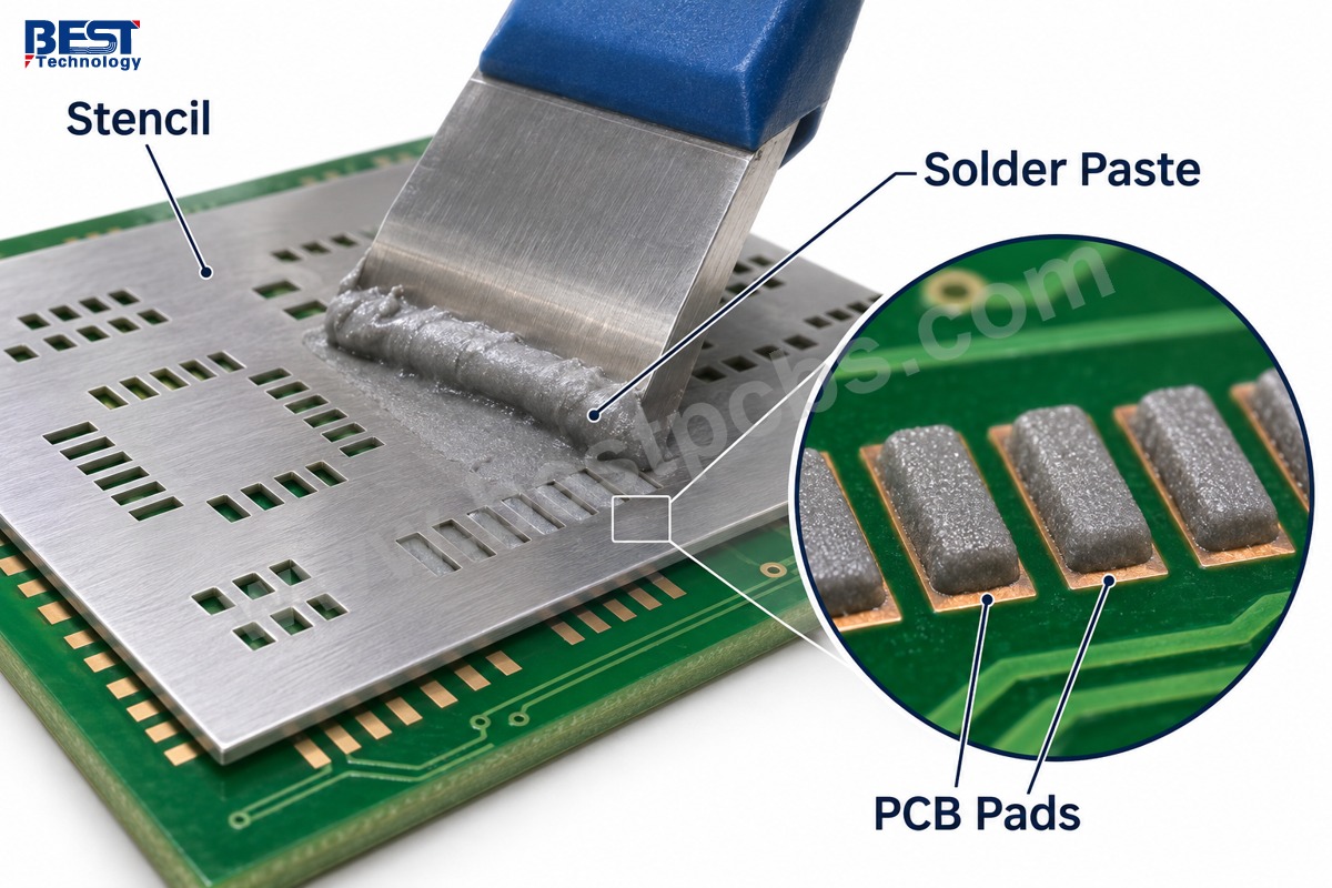
A board combining 01005 passives with a large power connector may need different paste deposits in different areas. Simply choosing a thicker stencil to supply the connector can overload the tiny pads. Aperture changes or a stepped stencil may be evaluated where the package mix requires them.
SPI gives measurable feedback on paste height, area, volume, and offset. Repeated low-volume deposits lead us to investigate aperture release, stencil contamination, support, or printing conditions. Repeated excess paste or bridging calls for a different correction. Inspection is most useful when it directs a process adjustment rather than becoming only a pass/fail gate.
What Reflow Temperature Does SMT Assembly Use?
A typical SAC305 lead-free process may use a solder-joint peak around 235–245°C, but the correct profile comes from the chosen paste specification, component limits, and measured temperatures on the actual board. This range is an example, not a universal oven recipe.
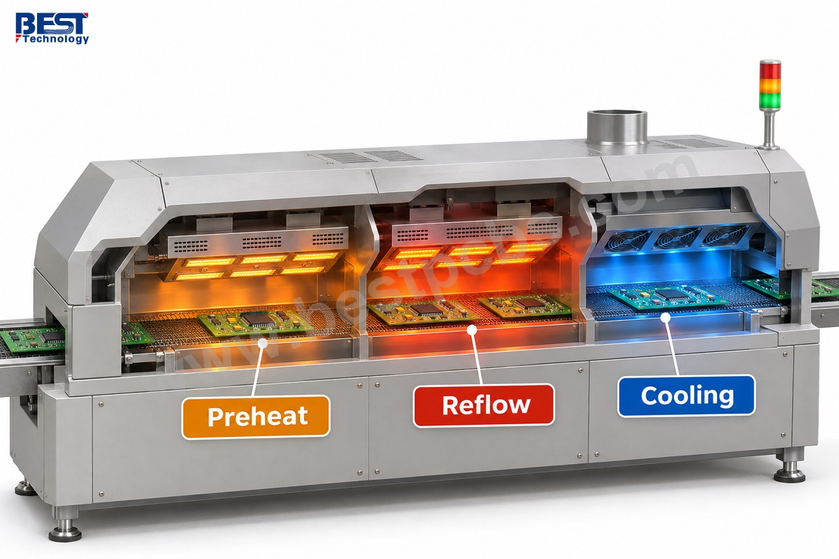
We evaluate the ramp, soak where applicable, time above liquidus, peak, and cooling behavior. Thermocouples at thermally different locations help reveal whether a large copper area or heavy component heats more slowly than a small passive. Raising the oven temperature without checking those locations can overheat sensitive parts while still leaving a difficult joint inadequately processed.
The recorded board temperature is different from an oven-zone setpoint. The selected alloy and flux system may also require a different profile from SAC305, so a lead-free classification by itself is not enough to select process settings.
How Are SMT Assemblies Inspected and Tested?
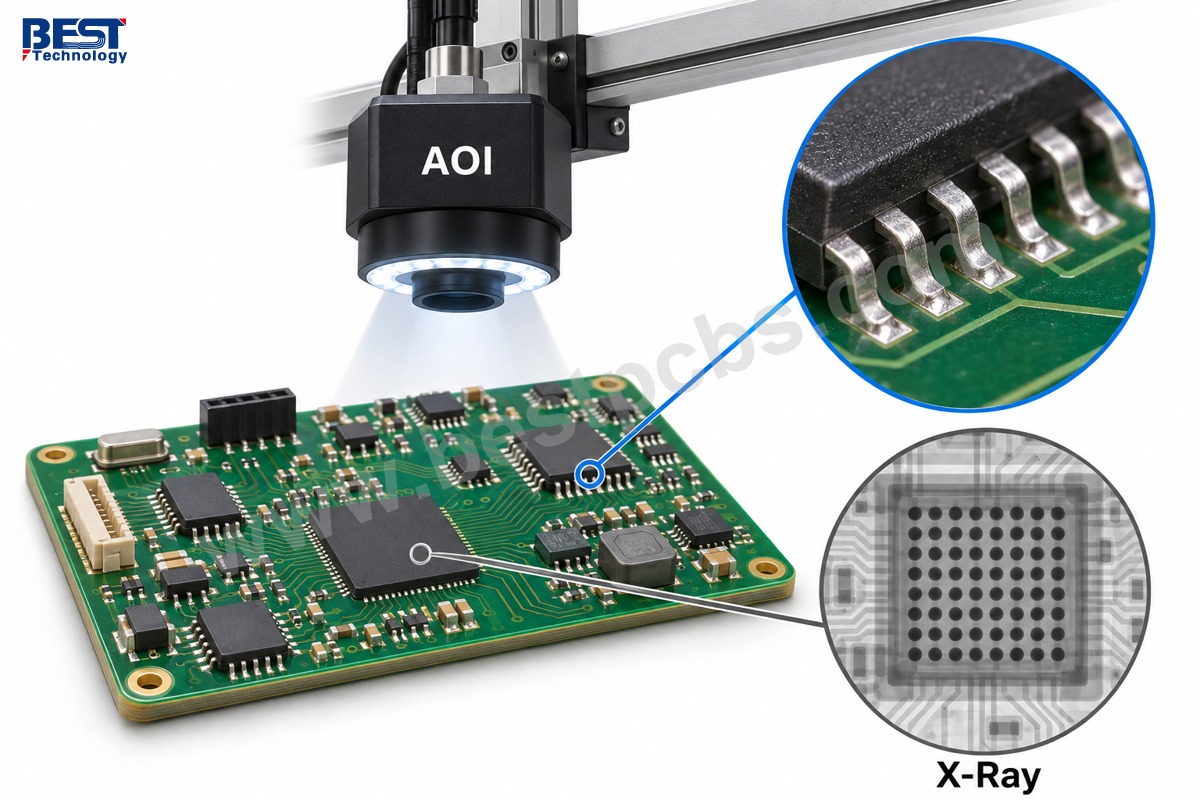
We use SPI for printed paste, AOI for visible assembly features, X-ray for specified hidden-joint checks, and functional testing for the behavior defined in the test plan. These methods address different defect mechanisms and should not be treated as interchangeable.
| Method | Inspection or Test Focus |
|---|---|
| 3D SPI | Paste volume, deposit height, area, offset before placement |
| AOI | Component presence, position, polarity features, visible solder-joint appearance |
| X-ray | Hidden-joint bridging, solder distribution and voiding where detectable with the selected technique |
| Functional testing | Specified power-up, communication, I/O, firmware and operating behavior |
For BGA and QFN builds, we agree on inspection coverage and acceptance criteria before production. A clear top-side image cannot establish the quality of every hidden joint, and a clean X-ray image does not establish that the firmware or circuit functions correctly.
Functional testing needs defined limits and a repeatable setup: supply voltage, current limits, firmware version, fixtures, and expected responses. We align the applicable workmanship requirements and customer criteria with the order rather than assuming every assembly requires the same acceptance class.
What Causes Common SMT Soldering Defects?
Common SMT defects come from incorrect paste deposits, placement errors, uneven heating, poor wetting, or package and board movement during ref low. The corrective action should address the cause, not just the visible solder joint.
| Defect | Typical Contributing Factors | Process Control |
|---|---|---|
| Solder bridging | Excess paste, poor alignment, insufficient separation | Review apertures, print offset, placement and lead condition |
| Tombstoning | Unequal wetting forces, uneven heating, paste imbalance | Review pad symmetry, copper balance, deposits and profile |
| Open joint | Insufficient paste, poor wetting, lifted lead or warpage | Check SPI, solderability, coplanarity and thermal behavior |
| QFN or BGA voiding | Flux outgassing, deposit pattern, pad design and profile interaction | Review stencil design and ref low; evaluate specified X-ray criteria |
A voiding limit must come from the relevant package, application, and acceptance requirements. A single percentage cannot be applied indiscriminately to every QFN thermal pad and every BGA joint.
What Affects SMT Assembly Cost and Lead Time?
Component availability, placement count, package difficulty, assembly sides, stencil requirements, inspection coverage, and test preparation are the main cost and scheduling drivers. A low component count does not automatically make a board easy to assemble if it contains a fine-pitch BGA or needs a custom test fixture.
Prototype orders spread stencil, programming, and setup work across fewer boards. Repeat orders can reuse approved production data and tooling when the design is unchanged. Cut-tape quantities, component attrition allowances, moisture-sensitive handling, and a second-side assembly also affect preparation.
For customers who want one team to coordinate boards, components, and assembly, our turnkey PCB assembly services bring those activities into the same project scope. We confirm the production schedule after reviewing material availability and the required manufacturing and test work.
Ready to Build Your Surface Mount Assembly?
At EBest Circuit, we review the manufacturing details that determine whether your design can move smoothly from prototype to production. Send your Gerber files, BOM, placement data, quantity, and test requirements to sales@bestpcbs.com. Tell us whether you need assembly only, component sourcing, or a complete PCB and PCBA build, and we will define the appropriate production scope with you.
FAQs About Surface Mount PCB Assembly
What is the difference between SMT and SMD?
SMT means surface mount technology, the manufacturing method. SMD means surface mount device, the component mounted using that method. A chip resistor is an SMD; printing paste and reflowing it onto a PCB is part of SMT.
Can one PCB combine surface-mount and through-hole components?
Yes. A mixed assembly can use SMT ICs and passives together with through-hole connectors or other parts. We plan the insertion and soldering sequence around the components and their heat restrictions.
Can I supply components instead of buying a full turnkey service?
Yes. We support consignment and partial turnkey builds. Supplied parts need clear part-number identification, usable packaging, and enough quantity for setup and the agreed attrition allowance.
Does no-clean solder paste mean the assembly never needs cleaning?
No. Cleaning depends on the qualified flux process and the product requirements, including coating compatibility, sensitive circuitry, and residue acceptance. The term no-clean does not override a customer’s cleanliness specification.
Can a prototype use the same SMT process as a production order?
Yes, when the package mix and build requirements support it. Using production-relevant stencil, placement, ref low, and inspection methods makes the prototype more useful for validating manufacturability before volume production.