What Is Solder Wicking in PCB Assembly? Solder wicking in PCB assembly is the unwanted movement of molten solder away from the intended solder joint. It usually happens because of capillary action, heat imbalance, open vias, exposed copper, improper solder paste volume, or unsuitable reflow conditions. When solder leaves the pad, the result may be a weak joint, dry joint, insufficient solder, open connection, or long-term reliability risk.
For EBest Circuit (Best Technology), solder wicking is not only a soldering term. It is a real PCBA quality issue that may appear in PCB SMT assembly, through-hole soldering, BGA assembly, via-in-pad structures, connector areas, and rework. If your PCB assembly project has solder joint, BGA, via-in-pad, SMT, stencil, reflow, or inspection concerns, please feel free to send your Gerber files, BOM, assembly drawing, PCB stackup, or soldering notes to sales@bestpcbs.com. Our engineering team can review the manufacturing path before production starts.
What Is Solder Wicking in PCB Assembly?
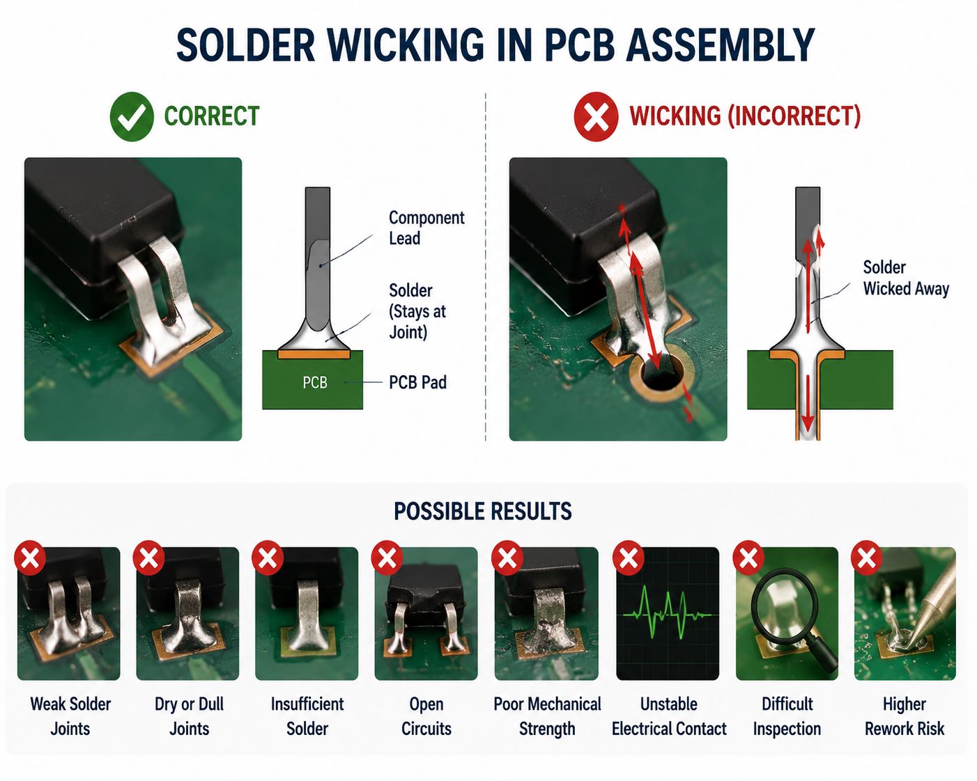
What is solder wicking? Solder wicking means molten solder is pulled away from the place where it should form a joint.
In PCB assembly, solder should stay between the component terminal and the PCB pad. If it flows into a via, up a component lead, along exposed copper, or into stranded wire, the solder volume left at the joint may become insufficient.
Common results include:
- weak solder joints
- dry or dull solder joints
- insufficient solder on pads
- open circuits
- poor mechanical strength
- unstable electrical contact
- difficult inspection results
- higher rework risk
Solder wicking is especially important in high-density PCBA projects because small pads, fine-pitch components, via-in-pad designs, BGA areas, connectors, and compact layouts leave less process margin.
Solder Wick vs Solder Wicking
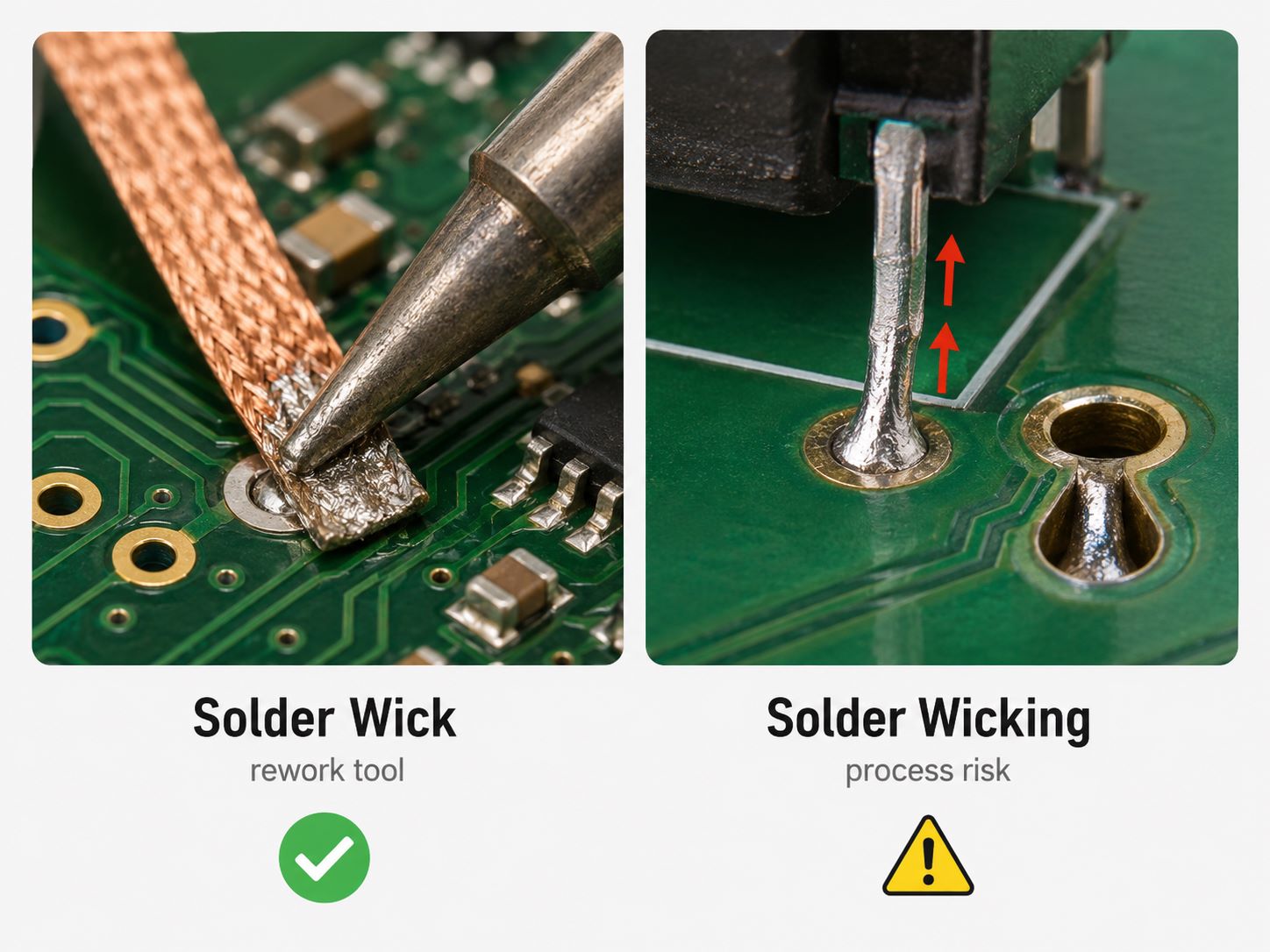
Solder wick and solder wicking sound similar, but they are not the same thing.
| Term | Meaning |
|---|---|
| Solder wick | A desoldering braid used to remove solder |
| Solder wicking | A solder flow defect or process risk |
| Desoldering wick | Another name for solder wick |
| Wicking solder | Solder being pulled away by capillary action |
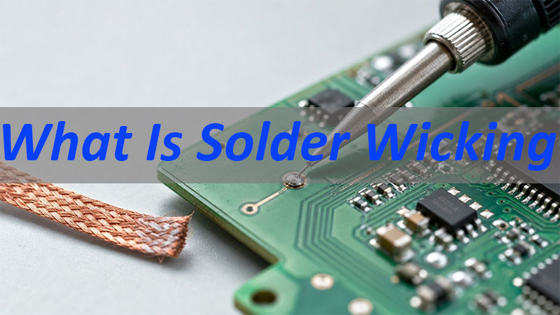
A solder wick is usually a braided copper strip with flux. It is used during rework or repair to remove extra solder from pads, bridges, or component leads.
Solder wicking, however, is usually unwanted. It means solder has moved away from the joint during soldering, reflow, wave soldering, hand soldering, or repair.
For PCB assembly projects, this distinction matters because the solution is different. Solder wick is a rework tool used to remove solder, while solder wicking is a process risk that should be prevented through PCB layout review, via control, solder mask design, stencil planning, and assembly inspection.
What Is Solder Wick Used For?
Solder wick is used to remove solder from a PCB during repair, prototype adjustment, or rework.
It is often used for:
- removing solder bridges
- cleaning pads before replacing components
- correcting excess solder
- removing solder from through-hole pads
- preparing pads for reassembly
- repairing prototype boards
- cleaning fine-pitch IC pads carefully
The basic working principle is simple. The heated solder melts, and the braided copper wick pulls the solder into itself through capillary action. Flux helps improve wetting and solder flow.
However, solder wick should be used carefully. Too much heat, too much pressure, or long contact time can damage pads, solder mask, copper traces, or nearby components. If rework is needed on a prototype or assembled PCB, the process should follow a controlled method for how to use solder wick and should be inspected after repair.
What Causes Solder Wicking on PCB Assemblies?
Solder wicking usually has more than one cause. It may come from PCB layout details, fabrication choices, assembly process settings, or repair conditions.
| Cause | What Happens |
|---|---|
| Open via near pad | Solder flows into the via |
| Via-in-pad not filled | Solder drains away from the component pad |
| Exposed copper path | Solder spreads beyond the joint |
| No solder mask dam | Solder moves toward nearby copper |
| Too much heat | Solder becomes too fluid |
| Long heating time | Solder keeps flowing before solidifying |
| Wrong paste volume | Joint receives too little or too much solder |
| Poor pad design | Solder balance becomes unstable |
| Wire strands | Solder climbs into the wire |
| Rework error | Excessive heat pulls solder away |
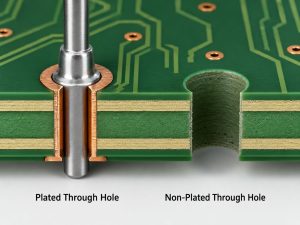
The core issue is usually capillary action. Molten solder is pulled into narrow spaces such as vias, gaps, copper braid, wire strands, or plated holes. If the PCB design or assembly process gives solder an easier path than the intended joint, wicking becomes more likely.
Solder Wicking in Via-in-Pad and BGA Assembly
Solder wicking is a serious concern in via-in-pad and BGA assembly.
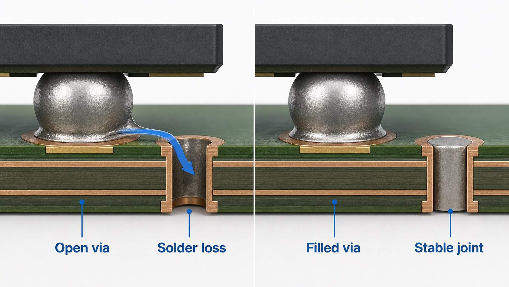
In a BGA area, vias may be placed inside or near pads to support dense routing. If those vias are open, solder can flow into the via during reflow. This may leave too little solder between the BGA ball and the pad.
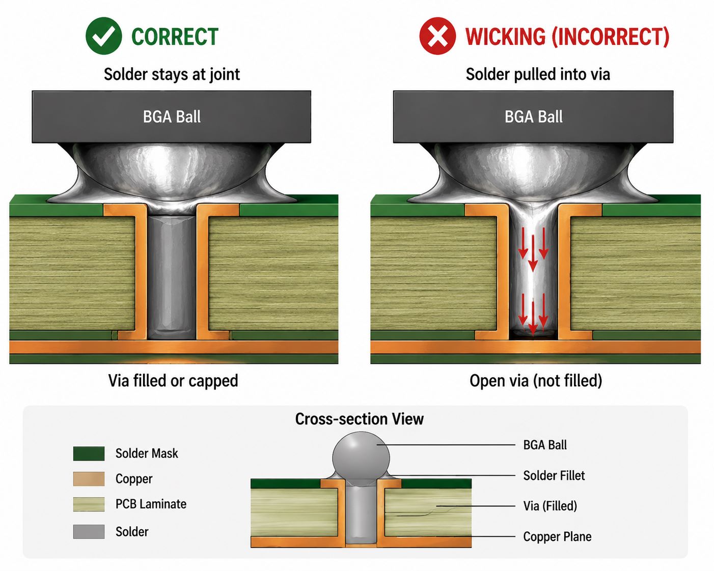
Possible problems include:
- weak BGA joints
- insufficient solder volume
- hidden opens
- poor coplanarity after reflow
- unreliable thermal cycling performance
- difficult X-Ray judgment
For via-in-pad designs, common manufacturing controls include resin-filled vias, plated-over vias, planarization, solder mask control, and proper pad definition. These points should be confirmed before PCB fabrication, not after SMT assembly.
For BGA-related projects, EBest Circuit can review whether the PCB fabrication process, via treatment, surface finish, solder mask opening, and assembly notes match the customer’s production requirements.
You may also refer to our guide on BGA soldering when reviewing BGA assembly risks.
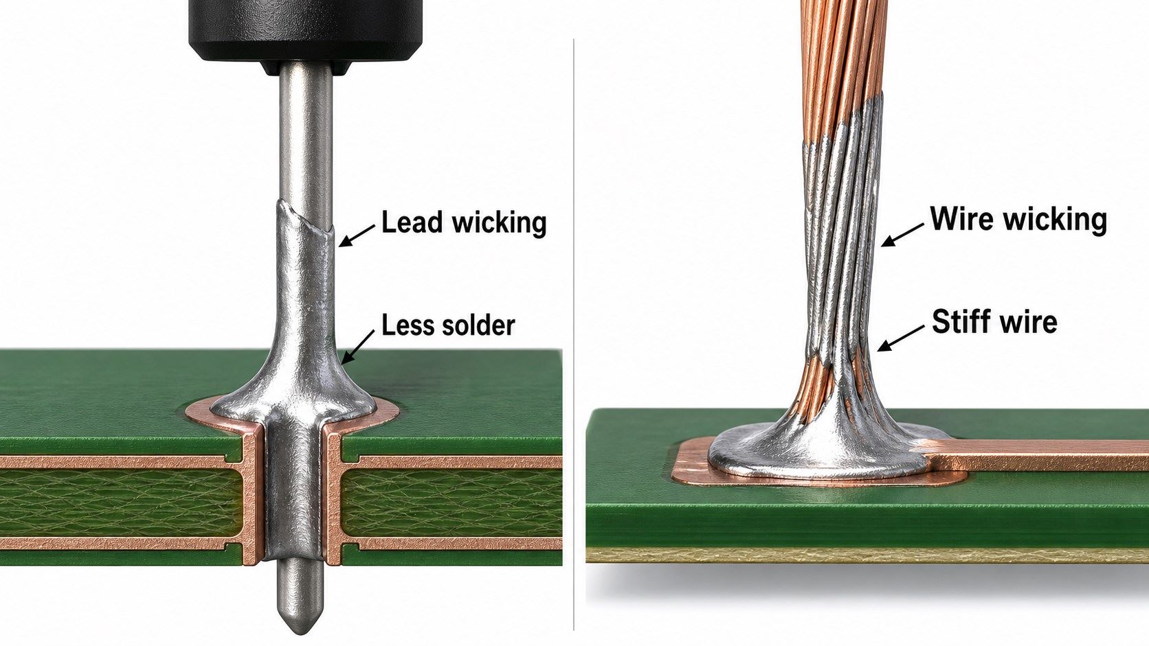
Solder Wicking in Through-Hole Components and Wires
Solder wicking can also happen in through-hole components and wires.
For through-hole components, solder may climb up the lead instead of staying around the plated through hole and pad. This can happen when the lead, hole size, heating time, flux activity, and solder volume are not balanced.
For stranded wires, solder can travel up the wire strands. A small amount of solder flow may be acceptable in some cases, but too much wicking can make the wire stiff. This may create mechanical stress near the solder joint, especially when the wire bends during use.
Areas that need attention include:
- connectors
- terminal blocks
- wire-to-board joints
- power input areas
- hand-soldered components
- reworked pads
- cable assemblies
- high-vibration applications
For PCBA projects with wires or through-hole parts, the assembly notes should clearly define soldering requirements, acceptable solder height, cleaning needs, inspection standard, and packing method.
How to Prevent Solder Wicking During SMT Assembly
Solder wicking prevention should start before production.
Useful checks include:
- keep vias away from pads when possible
- use filled and capped vias for via-in-pad
- maintain enough solder mask dam between pads and vias
- confirm pad size and solder mask opening
- review stencil aperture design
- control solder paste volume
- check reflow profile
- avoid excessive heating during rework
- inspect solder paste printing with SPI
- inspect finished solder joints with AOI or X-Ray when needed
For SMT assembly, the solder paste process is especially important. If paste volume is too low, the joint may be weak. If paste volume is too high, solder may bridge or flow into unwanted areas. The correct stencil design depends on pad size, component type, pitch, paste type, board finish, and assembly risk.
Reflow temperature also matters. A profile that is too aggressive may increase solder flow problems. A profile that is too weak may cause poor wetting. The right profile should match the solder paste, component thermal mass, PCB thickness, copper distribution, and assembly complexity.
You may also find our guide on solder temperature for PCB useful when reviewing soldering process conditions.
How to Inspect and Repair Solder Wicking Defects
Solder wicking defects should be checked at the right process stage.
Inspection methods may include:
- visual inspection
- SPI after solder paste printing
- AOI after reflow
- X-Ray for BGA, QFN, and hidden joints
- electrical testing
- functional testing
- microscope inspection for rework areas
A solder wicking defect may not always be obvious from the surface. In BGA or via-in-pad assembly, the problem may be hidden under the component. That is why X-Ray inspection is important for selected high-risk packages.
Repair depends on the defect type. Some joints can be corrected by controlled rework. Some BGA or via-in-pad issues may require component removal and reballing or replacement. If the root cause is open via-in-pad design or insufficient via filling, repair alone may not solve the problem for future batches.
A good repair process should answer three questions:
- Is the solder joint electrically reliable?
- Is the solder joint mechanically reliable?
- Has the root cause been corrected before the next build?
EBest Circuit PCBA Quality Control for Solder Wicking Risks
EBest Circuit controls solder wicking risks as part of the full PCB and PCBA manufacturing process.
Our support includes:
- DFM review before production
- PCB fabrication process review
- via-in-pad and resin-filled via review
- solder mask opening check
- BOM and assembly file review
- SMT process planning
- solder paste printing control
- SPI, AOI, and X-Ray support when required
- through-hole and hand soldering process control
- rework and inspection support
- prototype and small-batch production
This is important because solder wicking is not only an operator issue. It may come from the PCB structure, via design, pad design, solder mask, stencil, paste volume, reflow profile, component type, or rework method.
EBest Circuit provides one-stop PCB fabrication, component sourcing, PCBA assembly, testing coordination, and engineering review. For projects with BGA, fine-pitch ICs, via-in-pad, connectors, wire soldering, or high-reliability requirements, this integrated workflow helps keep manufacturing details visible from file review to final delivery.
FAQs about Solder Wicking and Solder Wick
1. What is solder wicking?
Solder wicking is the unwanted movement of molten solder away from the intended solder joint. In PCB assembly, it may cause insufficient solder, weak joints, dry joints, or open connections.
2. Is solder wick the same as solder wicking?
No. Solder wick is a desoldering braid used to remove solder. Solder wicking is a solder flow problem or defect where solder is pulled away from the joint.
3. What is solder wick used for?
Solder wick is used for removing solder bridges, cleaning pads, repairing prototype boards, and preparing pads for component replacement during rework.
4. How do you prevent solder wicking in PCB assembly?
Prevention methods include proper via placement, filled via-in-pad, solder mask dams, correct stencil aperture, controlled solder paste volume, suitable reflow profile, and inspection after SMT.
5. Why is solder wicking a problem in BGA assembly?
In BGA assembly, solder wicking may pull solder into open vias or away from pads. This can create weak or hidden solder joints that may require X-Ray inspection.
In summary, if your PCB or PCBA project involves BGA assembly, via-in-pad, fine-pitch SMT, through-hole soldering, connector soldering, rework, or solder joint quality concerns, please feel free to contact sales@bestpcbs.com. EBest Circuit’s engineering team can help review your files and manufacturing notes before production, so soldering risks are addressed earlier instead of discovered after assembly.