A solder fillet is the visible solder profile that joins a component termination to a PCB land. Its shape provides evidence of wetting, solder volume, alignment and process balance, but appearance alone cannot establish the electrical integrity or long-term reliability of every joint. Accurate evaluation depends on the termination type, package construction, product class, customer requirements and applicable acceptance criteria.
A sound evaluation starts with fillet formation and visible heel, toe and side profiles, then accounts for SMT, through-hole and package-specific differences. Pad design, solder volume, wetting and reflow explain many defects; inspection criteria, prevention and corrective action determine what happens next.
What Is a Solder Fillet and How Does It Form?
A solder fillet forms through wetting and solidification. Molten solder wets the PCB land and component termination, then solidifies into a continuous metallurgical connection. The visible curve is only the outside portion of the joint. Its final profile depends on solder volume, surface condition, geometry, gravity, surface tension, component standoff and the heating and cooling cycle.
SMT fillets form during solder-paste reflow. Solder paste is printed onto the lands, components are placed, and the assembly moves through reflow. The flux activates as temperature rises, helping remove light oxides. Solder particles melt, spread over solderable surfaces and pull the termination toward equilibrium. During cooling, the alloy solidifies and preserves the resulting fillet geometry.
Through-hole fillets form around a lead and plated barrel. Solder enters from the solder-source side during wave, selective or hand soldering. Wetting and capillary action help solder rise through the barrel and connect the lead, hole wall and land. The visible soldering fillet on either side must therefore be considered with barrel fill, circumferential wetting and lead condition.
Fillet formation follows a controlled sequence:
- Confirm that the land, finish and component termination are solderable and free of harmful contamination.
- Deposit or deliver the solder volume required by the footprint and termination.
- Align and support the component so its termination overlaps the intended land.
- Apply a thermal cycle that activates the flux and heats both joining surfaces sufficiently.
- Allow molten solder to wet and spread without movement, excessive oxidation or premature cooling.
- Cool the joint under controlled conditions, then inspect it against the correct criteria.
What Do Good Heel, Toe and Side Soldering Fillet Shapes Look Like?
Good fillets show continuous wetting and controlled solder volume. Heel, toe and side evidence must suit the lead and land geometry without hiding the joint or bridging adjacent conductors. A smooth concave transition is useful on many visible SMT joints, but it is not a universal acceptance template.
- Heel fillet: Look for a continuous transition at the inside bend or rear of a gull-wing lead. Gaps, cracks, lifted leads or a visibly starved joint require closer evaluation.
- Toe fillet: Where the termination design permits visible toe wetting, check the lead end and land for continuous coverage without bridges, solder balls or an excessive mound.
- Side fillet: Check both sides for consistent wetting, open edges, dewetting or asymmetry. QFN sidewalls may not wet unless the package has wettable flanks.
Fillet visibility depends on the termination geometry. A toe or side fillet is not equally visible or required for every termination, so package-specific criteria take precedence over a generic shape.
Do not judge a joint only by shine. Lead-free alloys can have a matte surface and still be acceptable, while a glossy joint can conceal incomplete wetting or excessive solder. Inspect the lead, land and solder as one connection. Compare both ends of two-terminal components because unequal fillet volume can indicate paste imbalance, component offset or uneven heating.
Excess solder at an MLCC termination can increase stress during board bending. The largest fillet is not automatically the best. The joint still needs sufficient wetting and solder volume within the component manufacturer’s land-pattern and mounting guidance.
Why Does Solder Fillet Geometry Affect Solder Joint Reliability?
Fillet geometry changes electrical and mechanical load transfer. Too little connected area can reduce mechanical margin or create an intermittent open. Excess solder can obscure evidence, bridge conductors, increase stress on fragile terminations or produce a shape that is difficult to inspect consistently.
A solder joint expands and contracts as the component and PCB cycle through temperature changes. Differences among the package, copper, laminate and solder concentrate strain in the interconnect. Joint height, cross-sectional area, lead compliance, alloy, pad size and package stiffness all affect that strain. Geometry contributes to reliability, but it cannot predict service life by itself.
A controlled CALCE study examined reworked surface-mount assemblies. Uneven and reduced joint heights affected temperature-cycling performance for the tested leadless resistor configuration, but the tested gull-wing package did not show the same response. The result is package- and test-specific; it does not establish a universal fillet-height limit.
Geometry must be evaluated against the assembly’s actual thermal, vibration and current loads. Visual acceptance does not prove service life. Products exposed to severe loads need application-appropriate electrical, mechanical or environmental validation in addition to fillet inspection.
How Do SMT and Through-Hole Solder Fillets Differ?
SMT and through-hole fillets form through different processes. SMT fillets form on surface lands through paste printing and reflow. Through-hole fillets form around leads and plated barrels during wave, selective or hand soldering. Their visible evidence and inspection requirements are not interchangeable.
| Comparison Dimension | SMT Solder Fillet | Through-Hole Solder Fillet |
| Connection geometry | Termination overlaps a surface land | Lead passes through a plated barrel |
| Primary solder source | Printed solder paste | Wave, selective nozzle or solder wire |
| Key design inputs | Land pattern, stencil aperture, mask and component standoff | Hole-to-lead relationship, annular land, barrel plating and lead protrusion |
| Visible evidence | Heel, toe and side wetting where accessible | Fillet, circumferential wetting and lead condition |
| Common defect drivers | Paste release, placement, coplanarity and reflow imbalance | Fluxing, preheat, wave contact, hole design and thermal demand |
| Typical inspection | Visual, AOI, 3D optical measurement and X-ray for hidden joints | Visual inspection plus barrel-fill or sectional evidence when required |
A through-hole joint is not acceptable merely because it forms a rounded mound. A large convex profile can hide poor wetting or incomplete barrel fill. An SMT chip joint should not be rejected simply because it lacks the cone-like shape of a through-hole joint. Use termination-specific acceptance criteria.
How Should QFN, Gull-Wing, J-Lead and Castellated Solder Fillets Be Evaluated?
Evaluate packages by visible surfaces and hidden-joint risk. Gull-wing leads offer relatively clear heel, toe and side views. J-leads hide part of the connection beneath the inward-curved lead. QFNs place most of the joint under the package, while castellated modules expose edge terminations for side-fillet inspection.
| Package or Termination | Visible Fillet Evidence | Hidden or Ambiguous Area | Primary Design/Process Concern | Verification Approach |
| Gull-wing lead | Heel, toe and both sides are often accessible | Interface directly beneath the lead | Lead coplanarity, paste volume and fine-pitch bridging | Controlled visual inspection or AOI with escalation for uncertain joints |
| J-lead | Outer side and portions of the lead-to-land transition | Connection under the curved lead | Placement, land length and limited viewing access | Multiple viewing angles; additional method if acceptance remains uncertain |
| QFN | Side fillet only where the termination design supports wetting | Bottom perimeter lands and exposed thermal pad | Stencil segmentation, paste balance, voiding, standoff and sidewall finish | AOI for visible flanks plus X-ray or other evidence for hidden connections |
| Castellated module | Side wetting along the plated half-hole and host-board land | Interface beneath the module edge | Castellation plating, land extension, coplanarity and paste release | Side-view optical inspection with electrical verification as required |
QFN inspection requires package-specific evidence. Some packages use wettable flanks specifically to promote visible side wetting and improve AOI discrimination. Other QFN sidewalls are not intended to wet in the same way. Limited side solder therefore does not automatically prove that the hidden bottom joint is defective. Check the component datasheet and package drawing before creating a local reject rule.
For a new footprint, compare the land pattern with the component manufacturer’s current recommendation. Confirm the exposed-pad design, paste segmentation, mask clearances and via treatment. A generic QFN footprint can create excess center-pad solder, package float or perimeter opens even when the reflow oven is functioning correctly.
How Do Pad Design, Solder Volume and Reflow Affect Solder Fillet Geometry?
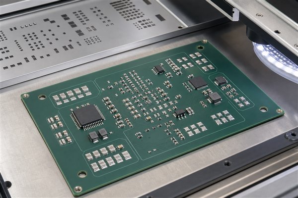
Pad geometry, solder volume and reflow act as one system. The pad defines where solder can spread, the stencil controls the deposited volume, and reflow determines whether the deposit wets and solidifies evenly. Oven settings cannot correct an unsuitable land pattern or blocked aperture.
Use the following sequence during design and process setup:
- Start with the package drawing. Verify termination dimensions, tolerances, standoff and the manufacturer’s recommended land pattern.
- Define the PCB lands. Provide the overlap and inspection access required by the component without creating unnecessary exposed copper or bridge risk.
- Coordinate solder mask. Check mask registration, dams and whether solder-mask-defined or non-solder-mask-defined geometry is appropriate for that feature.
- Design stencil apertures. Set deposit area and volume by package, pitch and thermal demand. Segment large thermal-pad apertures where appropriate instead of printing one uncontrolled mass.
- Verify paste release. Review aperture wall quality, stencil cleanliness, board support, squeegee conditions and paste condition.
- Control placement. Confirm centering, rotation, lead coplanarity and placement force so the part does not squeeze paste away or sit outside the wettable area.
- Develop a board-specific profile. Measure the loaded assembly rather than copying a profile from a different board. Respect solder-paste and component thermal limits.
- Correlate results. Compare SPI, placement, reflow and post-reflow inspection by reference designator before changing limits.
Thermal balance matters at both ends of a chip component. A pad connected to a large copper area may heat differently from a pad connected to a narrow trace. Unequal melting and wetting forces can create uneven fillets or tombstoning. Review thermal relief, copper balance, aperture design and the reflow profile as one system.
What Causes Insufficient, Missing, Excessive or Uneven Solder Fillets?
Fillet defects usually start in delivery, wetting, placement or heat. Joint disturbance can add another failure path. Diagnose the visible symptom by confirming its location, repetition pattern and upstream process changes.
| Observed Fillet Condition | Likely Cause Categories | Evidence to Check | Risk or Limitation | Corrective Direction |
| Insufficient solder fillet | Low paste volume, poor release, undersized aperture, component/land mismatch | SPI volume, stencil opening, paste transfer and joint location pattern | Reduced connection area or intermittent/open behavior | Restore controlled deposit and confirm footprint compatibility |
| Missing fillet | Blocked aperture, severe nonwetting, missing paste or lifted termination | Pre-placement paste image, AOI image, lead coplanarity and surface condition | A hidden joint may still exist on some packages; visibility alone is inconclusive | Separate deposition failure from package-visibility limitation |
| Excessive solder fillet | Oversized aperture, thick stencil, duplicate solder addition or poor drainage | Deposit volume, rework history, bridge clearance and component seating | Can hide wetting, bridge conductors or stress fragile terminations | Reduce or redistribute volume without starving the joint |
| Uneven fillets | Paste imbalance, placement offset, unequal thermal mass or pad asymmetry | Paired-pad SPI data, centroid, copper connections and profile traces | May indicate unequal load transfer or impending tombstoning | Balance design, printing, placement and heating |
Defect patterns help isolate the failing process stage. If the same lead or reference designator is affected on multiple boards, first check the footprint, aperture and local copper. If missing or insufficient deposits occur randomly, examine stencil cleaning, paste roll condition, board support and printer stability. If acceptable SPI is followed by a poor joint, move the investigation to placement, solderability and reflow.
How Do Poor Wetting and Dewetting Affect Solder Fillet Shape?
Nonwetting leaves the basis metal exposed. Molten solder contacted the surface but did not form the required bond. Dewetting occurs after solder initially covers the surface and then recedes, leaving irregular solder mounds separated by thin solder-covered areas.
Wetting barriers are not solved by heat alone. Common causes include oxides, contamination, degraded finishes, insufficient flux activity and inadequate heat at the actual joint. Excessive time or temperature can also damage flux performance or promote surface reactions that worsen the result. Inspect storage history, finish condition, paste handling and measured thermal response before changing the profile.
Contact angle is evidence, not a universal limit. A large angle can warn that solder has not spread effectively, but three-dimensional geometry, viewing direction and component construction affect the measurement. Use it alongside continuous wetting, solder coverage, land/lead geometry and the applicable acceptance document.
Do not repeatedly reflow a poorly wetted joint. Extra heating can damage the pad, laminate or component and may create intermetallic growth without restoring a clean solderable interface. Quarantine the affected material, compare known-good samples, verify surface condition and approve any rework through a controlled instruction.
How Are Solder Fillets Inspected Against IPC Acceptance Criteria?
Inspect each fillet against termination-specific criteria. Apply the required product class, customer requirements and a method capable of seeing the relevant feature. IPC J-STD-001J defines soldered-assembly process and material requirements, while IPC-A-610J defines post-assembly acceptability criteria.

Do not apply IPC criteria from an unrelated package. Before inspection, identify the assembly revision, product class, termination type and any customer-approved deviations. Use the current purchased standard and contract documents for the actual acceptance limits.
| Inspection Method | What It Evaluates | Best-Fit Fillets or Packages | Limitation | Escalation Trigger |
| Controlled visual inspection | Accessible wetting, cracks, bridges, solder quantity and lead position | Through-hole, gull-wing, castellated and accessible chip joints | Cannot prove hidden structure or electrical continuity | Obscured interface, borderline condition or repeat defect |
| 2D/3D AOI | Visible geometry, component placement and programmed anomalies | Production SMT with repeatable visible features | Program limits and lighting can create false calls or escapes | Hidden joint, uncertain side wetting or changing false-call rate |
| X-ray inspection | Hidden solder distribution, opens, bridges and selected void evidence | QFN, BGA, LGA and other bottom-terminated packages | A 2D projection may overlap structures and does not show every interface condition | Ambiguous image, critical defect or root-cause investigation |
| 3D optical measurement | Height, profile, area and repeatable visible geometry | Accessible fillets requiring quantitative comparison | Cannot see beneath an opaque package | Correlation with destructive analysis is needed |
| Cross-section | Internal interface, joint thickness, wetting and defect morphology | Failure analysis and process validation samples | Destructive and limited to the sampled location | Unresolved systemic defect or qualification need |
Inspection records must support traceable disposition. Identify the board, lot, reference designator, method, viewing conditions, applicable criterion and disposition. Store representative images when they support the decision, and correlate them with SPI and process records where possible. The solder joint inspection guide explains how to select visual, AOI, X-ray and destructive methods by defect visibility.
How Can Solder Fillet Defects Be Prevented During PCB Assembly?
Prevent defects by controlling the complete assembly chain. Control the footprint, material condition, solder deposition, placement and reflow, then use inspection feedback to identify recurring variation.
Use this production sequence:
- Review the design. Check component drawings, land patterns, copper balance, mask clearances, thermal pads, vias and through-hole geometry before releasing fabrication data.
- Confirm incoming condition. Protect PCB finishes and component terminations from contamination, moisture and uncontrolled storage exposure.
- Control and measure solder delivery. Verify stencil thickness, aperture design, paste condition, printer setup, board support and cleaning frequency. Use SPI where appropriate to detect missing, low, excessive or offset deposits before placement. The solder paste stencil guide covers recurring printing defects.
- Control component placement. Verify package orientation, centroid data, nozzle selection, placement force and lead coplanarity.
- Develop the thermal process. Profile the populated assembly, including thermally demanding locations, and work within material and component limits.
- Inspect and correlate results. Program AOI by package and product revision, use X-ray or another suitable method for hidden joints, and correlate SPI, placement, reflow and inspection results by board and reference designator.
- Control rework. Use approved materials, tools, temperature limits and verification steps. Repeated heating without root-cause removal can create new damage.
- Close the corrective-action loop. Confirm that the change removes the defect without causing bridging, component stress, voiding or another unintended condition.
Prevention must remain package-specific. Increasing paste may repair an insufficient gull-wing fillet but cause float or voiding under a QFN thermal pad. Raising peak temperature may improve one cold location but exceed a sensitive component’s limit elsewhere. Change one justified variable, verify the result across the board and retain the evidence needed for repeat production.
How Should an Insufficient Solder Fillet Problem Be Corrected in SMT Production?
Find where solder volume is lost before changing the process. Determine whether a recurring insufficient fillet begins during printing, placement, wetting or reflow, then use the following sequence to verify the correction.
- Contain the suspect lot. Identify affected boards and reference designators, then prevent uncertain assemblies from advancing without disposition.
- Confirm the defect definition. Compare the joint with the correct termination criteria and known-good samples. Exclude a package-visibility issue before calling the fillet missing.
- Map the pattern. Determine whether the condition repeats on the same pad, one board region, one stencil cycle or random locations.
- Review pre-reflow evidence. Check paste presence, area, height, volume and offset where SPI or retained images are available.
- Inspect the stencil and support. Look for aperture blockage, damaged walls, contamination, board flex or poor gasketing at the affected land.
- Verify component placement. Confirm centering, rotation, coplanarity and placement force. A lead outside the paste deposit can resemble a printing problem after reflow.
- Check solderability and heat. Compare finish condition, flux performance and measured profile at the affected location.
- Apply the smallest justified change. Clean or repair the stencil, correct support or alignment, adjust the aperture through engineering control, or revise the board-specific profile according to the confirmed cause.
- Run a controlled confirmation lot. Verify deposit and post-reflow fillet evidence at the target location while checking neighboring joints for excess solder, bridging or component movement.
- Update controlled records. Revise the stencil, program, work instruction or inspection limits only after the corrective result is repeatable and approved.
Adding solder does not prevent recurrence. Close the corrective action only after the confirmed cause, controlled change, verification result and repeat-build instruction agree.
FAQs About Solder Fillet
Q1: Can a solder fillet be accepted from a smartphone photo?
A1: Not as the sole acceptance record. An uncontrolled photo may hide scale, viewing angle, lighting and depth. Use controlled magnification, the correct termination criterion and the board’s traceable inspection record.
Q2: Can flux residue be mistaken for a solder fillet defect?
A2: Residue can obscure edges, contamination or fine bridging. Inspect under suitable lighting and magnification. Clean only when the assembly process and materials permit it, then reinspect the same location.
Q3: Should a board with a suspect fillet be electrically tested before disposition?
A3: Contain and assess the risk first. If the condition may create a short, lifted conductor or unstable connection, follow the approved inspection and disposition process before applying power.
Q4: What solder-joint requirements should a purchase order specify?
A4: Specify the governing acceptance requirements. State the standard revision, product class, customer-specific criteria, approved deviations, inspection records and required tests.
Q5: Should solder fillets be inspected before conformal coating?
A5: Inspect before coating obscures the joints. Retain images or machine records for locations that will be difficult to verify after coating.
Q6: How many times can a defective solder fillet be reworked?
A6: There is no universal rework count. The limit depends on the PCB, finish, component and approved repair instruction. Repeated heating can damage pads, laminate, coatings or the component.
Q7: How should AOI limits be established for a new package?
A7: Start with package data, criteria and controlled samples. Validate lighting and viewing angles with known acceptable and defective conditions, then place threshold changes under revision control.
Q8: When should PCB or component solderability be tested?
A8: Test after repeated, unresolved wetting failures. Separate PCB-finish evaluation from component-termination evaluation and use an agreed method.
Q9: Does a cleanliness test prove that a solder fillet is acceptable?
A9: No; cleanliness and joint acceptability are different attributes. Cleanliness testing evaluates residues under its test method, while fillet acceptance still requires termination-specific inspection and any required electrical evidence.
For an engineering review and quotation, send your Gerber or ODB++ files, BOM and placement data to EBest Circuit at sales@bestpcbs.com. Include the quantity, package requirements and acceptance criteria.