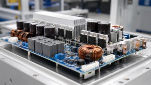
Proto board is often one of the first tools engineers, makers, and product developers use when turning a circuit idea into something they can test on the bench. It gives you a practical way to place components, connect signals, check power paths, and verify whether a circuit behaves as expected before investing in a custom PCB.
For early-stage development, this approach is flexible and cost-friendly. You can adjust wiring, replace components, test different values, and improve the circuit step by step. Once the design becomes stable, the next step is usually a more reliable PCB prototype that can support repeatable testing, better assembly quality, and pilot production.
This guide explains what a proto board is, how it works, how it compares with breadboards and PCB prototypes, how to use and solder it properly, and when it makes sense to move from hand-built wiring to a custom manufactured circuit board.
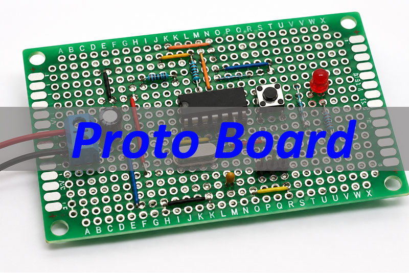
What Is a Proto Board?
A proto board is a board used to build and test electronic circuits before creating a final PCB design. It usually contains a grid of holes, copper pads, or plated-through areas where components can be inserted, soldered, and connected with wires or solder bridges.
It is also commonly called a prototype board, prototyping board, or protoboard. These terms are often used in similar contexts, although the exact board structure can vary. Some boards are plain perfboards with individual pads, while others follow a breadboard-like pattern that makes circuit transfer easier.
A proto board is useful because it sits between two development stages:
| Development Stage | Typical Tool | Main Purpose |
|---|---|---|
| Concept testing | Breadboard | Quick, temporary circuit experiments |
| Functional validation | Proto board | More stable soldered prototype |
| Product verification | Custom PCB prototype | Repeatable layout, dimensions, and performance |
| Production | Fabricated PCB / PCBA | Scalable manufacturing and assembly |
In simple terms, a proto board helps you move from “the circuit works in theory” to “the circuit works in hardware.”
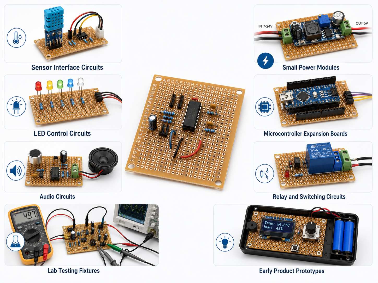
It is widely used for:
- Sensor interface circuits
- Small power modules
- LED control circuits
- Microcontroller expansion boards
- Audio circuits
- Relay and switching circuits
- Lab testing fixtures
- Early product prototypes
For simple circuits, a proto board can be enough for long-term bench use. For commercial products, however, it is usually a development step before a custom PCB prototype.
When Should You Use One in Electronics Prototyping?
A proto board is most valuable when your circuit has moved beyond a quick breadboard test but is not ready for formal PCB fabrication yet. It gives you more mechanical stability than jumper wires on a breadboard while still allowing design changes.
You can use it when:
- The schematic is mostly confirmed
- The circuit needs soldered connections for stable testing
- The prototype will be handled, moved, or tested repeatedly
- The design uses through-hole components
- You want to test connector positions before layout design
- The circuit is small enough for manual wiring
- You are validating a module before creating a full PCB
For example, an engineer may test a temperature sensor circuit on a breadboard first. After confirming the sensor output and microcontroller code, the same circuit can be transferred to a proto board for longer functional testing. This gives stronger connections and fewer loose wire issues.
A proto board is also helpful when evaluating component values. You can test different resistors, capacitors, connectors, or interface parts before locking the design into a PCB layout. That flexibility is one reason it remains popular in engineering labs, schools, repair benches, and product development teams.
For dense circuits, high-speed signals, RF designs, thermal-sensitive power boards, or products that require enclosure fitting, a custom PCB prototype is usually a better next step.
How Does a Proto Board Connect Components?
A proto board connects components through copper pads, plated holes, jumper wires, solder joints, or copper traces depending on the board style.
Most basic boards have individual copper pads around each hole. Components are inserted through the holes and soldered to the pads.
The electrical connections are then created manually with:
- Solder bridges
- Solid-core jumper wires
- Insulated hookup wires
- Bare copper wires
- Pre-designed copper strips
- External connectors
Some boards are designed to imitate a breadboard layout. These make it easier to transfer a working breadboard circuit into a soldered format. Other boards are completely open-grid, giving engineers more layout freedom.
A clean build usually starts with the main components first. Connectors, IC sockets, regulators, switches, and larger capacitors are placed before smaller passive parts. After that, power, ground, and signal paths are wired carefully.
The key is to think of the board as a manual circuit layout.
Even though it is hand-wired, the same engineering logic still applies:
- Keep power paths clear
- Keep ground connections short and stable
- Avoid crossing too many signal wires
- Separate noisy and sensitive areas
- Leave room for test points
- Mark pin functions and polarity
- Inspect each connection before power-on
A proto board may look simple, but poor wiring can affect circuit behavior. A clean layout gives better test results and makes troubleshooting easier.
Breadboard, Perfboard, and PCB Prototype Board: What Is the Difference?
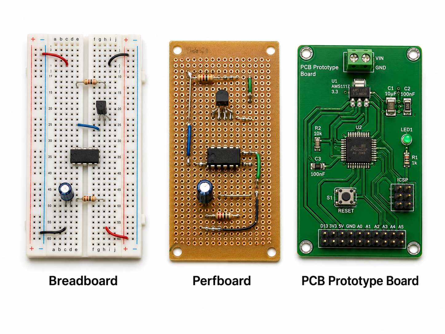
Breadboards, perfboards, proto boards, and PCB prototype boards are all used during development, but they serve different purposes. Choosing the right one depends on where you are in the design process.
| Board Type | Best For | Connection Method | Reusable | Stability |
|---|---|---|---|---|
| Breadboard | Fast circuit experiments | Jumper wires and internal clips | Yes | Low to medium |
| Perfboard | Manual soldered circuits | Point-to-point soldering | Usually no | Medium |
| Proto board | Stable functional prototypes | Soldering, wiring, or copper pads | Usually no | Medium to high |
| PCB prototype board | Pre-production validation | Designed copper traces | No | High |
- A breadboard is best for very early testing. It allows fast changes without soldering. The trade-off is that jumper wires can become loose, contact resistance may vary, and layout control is limited.
- A perfboard is a perforated board with holes and copper pads. It gives a permanent soldered structure, but every electrical connection is usually made by hand.
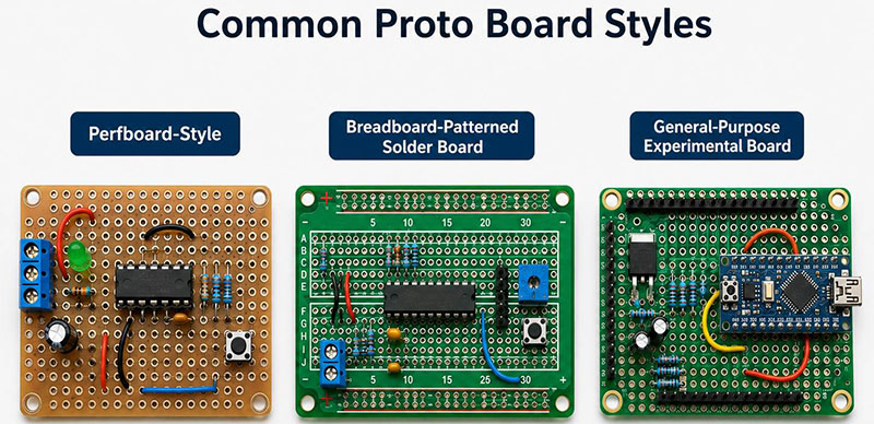
- A proto board can refer to several prototype board styles, including perfboard-like designs, breadboard-patterned solder boards, and general-purpose experimental boards. It gives more stability than a breadboard while keeping flexibility.
- A PCB prototype board is different because it is designed from CAD files and manufactured with defined copper traces, solder mask, drill holes, surface finish, and controlled dimensions. It is the better option when the design needs repeatability, assembly control, and product-level testing.
For early learning or small experiments, a breadboard or proto board works well. For engineering validation, customer samples, pilot runs, or commercial hardware, a custom PCB prototype gives a more dependable result.
Which Type of Prototype Board Should You Choose?
Different prototype boards are designed for different development tasks. Instead of choosing only by size or price, it is better to choose based on the circuit type, component package, wiring density, and testing goal.
- For through-hole circuits, a standard proto board or perfboard is often the easiest choice. It works well for resistors, DIP ICs, headers, switches, connectors, relays, and electrolytic capacitors.
- For surface-mount components, an SMD prototype board is more suitable. These boards include pad patterns for common packages such as SOIC, SOT-23, 0805, 0603, QFN adapters, or other small footprints. They are useful when testing modern ICs that are not available in through-hole packages.
- For development boards, Arduino or Raspberry Pi expansion boards can speed up testing. They provide compatible header spacing and make it easier to connect sensors, modules, displays, or driver circuits.
- For compact circuits, a mini prototype board saves space and works well for small sensor modules, LED circuits, or simple interface boards.
- For lab use, a proto board kit can be practical. It often includes different board sizes, headers, jumper wires, terminal blocks, and small accessories for daily testing.
When the circuit becomes complex, manually selecting a larger proto board is not always the best answer. At some point, the project benefits more from a custom PCB layout with fixed routing, correct footprints, mounting holes, and cleaner assembly.
How to Build a Simple Circuit Step by Step
Building a circuit on a proto board is easier when the process is organized. A good workflow prevents messy wiring and reduces debugging time.
1. Review the schematic first
- Start with a clear schematic. Confirm component values, pin numbers, power input, ground points, connector orientation, and signal direction before placing anything on the board.
2. Place the main components
- Put larger or more important parts first. IC sockets, connectors, switches, regulators, relays, and terminal blocks should be positioned with enough spacing around them.
3. Plan the power and ground paths
- Power and ground should be easy to identify. Use thicker wires for higher current paths and avoid routing power through thin, weak connections.
4. Group related components
- Place supporting resistors, capacitors, and protection parts close to the IC or connector they support. This makes the circuit easier to read and improves electrical behavior.
5. Add signal connections carefully
- Use short and direct wires where possible. For analog or sensitive signals, keep them away from switching nodes, relays, motors, and high-current paths.
6. Solder in stages
- Do not solder everything at once. Complete one section, inspect it, then move to the next. This makes mistakes easier to find.
7. Check continuity before applying power
- Use a multimeter to confirm power, ground, and important signal paths. Check for shorts between power and ground before turning the circuit on.
8. Power up gradually
- If possible, use a current-limited power supply. Start with a low current limit, then verify voltage rails and key signals step by step.
This process turns a hand-built circuit into a more controlled engineering sample. It also creates useful reference information for the later PCB layout stage.
Layout, Wiring, and Soldering Tips for a Cleaner Build
A well-built proto board is easier to test, modify, and convert into a PCB design. The goal is not only to make the circuit work, but to make it understandable.
Keep the layout readable
- Place the circuit in a logical direction. For example, power input can start from one side, signal input from another side, and output connectors near the edge. This makes testing and troubleshooting more efficient.
Use short wiring where possible
- Long jumper wires add clutter and can pick up noise. Shorter wires make the board stronger and cleaner.
Separate power and signal paths
- Power circuits, switching circuits, and motor drivers can introduce noise. Keep sensitive analog lines, sensor signals, and communication traces away from these areas.
Mark important pins
- Label voltage input, ground, signal pins, polarity, and connector direction. Even simple labels can prevent mistakes during testing.
Use good soldering practice
- A proper solder joint should be smooth, shiny, and mechanically stable. Cold solder joints, excess solder, and weak pad connections can create intermittent faults.
Leave space for test points
- Add accessible points for measuring voltage, current, PWM signals, I2C, SPI, UART, reset lines, and sensor outputs. Debugging is much easier when test access is planned.
Inspect before each major test
- A visual inspection and continuity test can catch many problems early. Look for solder bridges, reversed components, loose wires, wrong pin connections, and overheated pads.
For simple low-speed circuits, these tips are often enough. For RF circuits, high-speed digital interfaces, precision analog boards, or power electronics, a custom PCB prototype gives better control over impedance, grounding, thermal paths, and repeatability.
When Should a Prototype Become a Custom PCB?
A working hand-wired prototype is an important milestone, but it is usually not the final hardware format. Once the circuit has been verified, a custom PCB makes the design cleaner, stronger, and easier to reproduce.
You should consider moving to a custom PCB when:
- The circuit function has been confirmed
- Wiring becomes crowded or difficult to trace
- The same board must be tested several times
- Connector location and board size matter
- The product must fit inside an enclosure
- The circuit includes high-speed, RF, or noise-sensitive signals
- Thermal performance becomes important
- The project is moving toward pilot production
- Assembly time is becoming too long
- The design requires consistent quality across multiple units
A custom PCB prototype allows the copper traces, component footprints, mounting holes, solder mask, silkscreen, and surface finish to be controlled. It also makes PCBA assembly more practical.
This step is especially valuable when a product team wants to reduce hand-wiring errors, improve test consistency, and prepare for customer samples or small-batch production.
Before production, the design should go through proper engineering review. Gerber files, drill files, stackup, copper spacing, solder mask clearance, component footprints, BOM availability, and assembly requirements should all be checked. This is where a professional PCB manufacturer can add real value.
Case Study: 4-Layer FR4 PCB Prototype from a Customer’s Proto Board Project
After testing the circuit on a proto board, the customer wanted a more stable PCB prototype for the next development stage. The hand-wired prototype had already proved the basic function, but it was not suitable for repeat testing, assembly review, or small-batch preparation.
To move the project forward, we manufactured a 4-layer FR4 PCB prototype based on the customer’s confirmed design files.
Customer Requirement
The customer needed a board that could provide:
- More reliable electrical connections than hand wiring
- A fixed layer structure for engineering validation
- Stable board thickness for assembly and enclosure checking
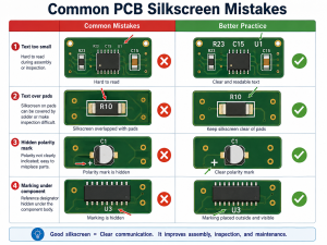
- Clear solder mask and silkscreen for component identification
- A practical surface finish for prototype testing
Our Manufacturing Support
Before production, our engineering team reviewed the PCB files and confirmed the key manufacturing details, including layer count, material grade, copper thickness, board thickness tolerance, solder mask, silkscreen, and surface finish.
For this project, we used FR4 TG170 material to provide better thermal stability during soldering and assembly. The board was produced with 1 oz copper on all four layers, which offered a balanced structure for prototype-level testing.
The board also used green solder mask, white silkscreen, and lead-free HASL surface finish, making it practical for engineering samples, functional testing, and further design review.
Project Specification
| Item | Specification |
|---|---|
| PCB Type | 4-Layer FR4 PCB |
| Material | FR4 TG170 |
| Copper Thickness | 1/1/1/1 oz |
| Board Thickness | 1.6 mm ±10% |
| Solder Mask | Green |
| Silkscreen | White |
| Surface Finish | Lead-Free HASL |
| Production Stage | PCB Prototype / Engineering Validation |
Result
The finished PCB gave the customer a cleaner and more repeatable platform than the original proto board. It helped the project move from early circuit testing to a more controlled PCB prototype stage, ready for assembly review, functional testing, and future small-batch production.
Why Choose Us for PCB Prototype Manufacturing After Proto Board Testing?
After a circuit works on a proto board, the next challenge is turning it into a manufacturable PCB. This step requires more than simply drawing copper traces. A reliable manufacturing partner should help review the design from fabrication, assembly, sourcing, and testing perspectives.
At EBest Circuit, we support customers from early PCB prototype to PCBA assembly and small-batch production. Our team can help convert verified prototype concepts into practical circuit boards with better layout control, cleaner assembly, and stronger production readiness.
Engineering Support Before Production
- We can review Gerber files, stackup, copper spacing, drill design, solder mask clearance, impedance requirements, component footprints, and assembly risks before production starts. This helps reduce avoidable issues before boards enter fabrication.
From PCB Prototype to PCBA Assembly
- Once your circuit has been tested on a proto board, we can support the next stage with PCB fabrication, component sourcing, SMT assembly, through-hole assembly, inspection, functional testing, and box-build assembly when required.
DFM Review and BOM Optimization
- A hand-built circuit may work electrically, but it still requires manufacturability review before it becomes a stable PCB. We can help check layout risks, part availability, alternative components, assembly feasibility, and production consistency.
Support for Different PCB Technologies
- Depending on your project, we can manufacture FR4 PCB, high-Tg PCB, aluminum PCB, copper-based PCB, ceramic PCB, Rogers high-frequency PCB, rigid-flex PCB, heavy copper PCB, and multilayer PCB.
Controlled Quality Process
- Our production support can include material control, drilling inspection, solder mask control, surface finish inspection, electrical testing, AOI, X-ray inspection when required, and functional testing for assembled boards.
One-Stop Service for Product Development
- For engineering teams, one-stop support reduces communication gaps between PCB fabrication, component sourcing, assembly, and testing. It also helps the project move from bench prototype to repeatable hardware with fewer handoff problems.
If your circuit has already been verified on a proto board, we can help you take the next step. Send your schematic, Gerber files, BOM, or prototype photos to our team for review and quotation.
FAQs About Proto Board
Q1: Is a proto board the same as a breadboard?
A1: Not exactly. A breadboard is usually solderless and reusable, while a proto board is commonly used for soldered prototypes. A breadboard is better for quick experiments, and a proto board is better for a more stable circuit build.
Q2: Can you solder components directly on a proto board?
A2: Yes. Most proto boards are designed for soldering through-hole components, wires, headers, connectors, and small modules. For surface-mount parts, an SMD-compatible prototype board or adapter board is usually more suitable.
Q3: What is the difference between a proto board and a PCB prototype board?
A3: A proto board is usually hand-wired or manually soldered. A PCB prototype board is manufactured from design files with defined copper traces, drilled holes, solder mask, surface finish, and board dimensions. The PCB version is more repeatable and better for product validation.
Q4: Can a proto board be used for SMD components?
A4: Yes, but it depends on the board type. Standard through-hole boards are not ideal for small SMD packages. For SMD testing, use a board with matching surface-mount pads or an adapter module.
Q5: How do you test a proto board before powering it on?
A5: Start with visual inspection, then use a multimeter to check continuity, power-to-ground shorts, component polarity, and important signal paths. For safer testing, power the circuit with a current-limited supply.
Q6: Is a proto board suitable for high-speed or RF circuits?
A6: It can be used for very basic experiments, but high-speed and RF circuits usually require controlled layout, impedance design, grounding strategy, and material selection. A custom PCB prototype is usually better for those applications.
Q7: When should I convert a proto board design into a custom PCB?
A7: Convert it when the circuit function is verified, wiring becomes dense, board size matters, testing must be repeatable, or the project is moving toward pilot production. This step helps improve reliability, assembly quality, and product readiness.
Q8: Can you manufacture a PCB prototype based on my proto board circuit?
A8: Yes. If you can provide the schematic, connection notes, photos, BOM, or existing layout idea, our engineering team can help review the design and support PCB prototype manufacturing, component sourcing, PCBA assembly, and testing.
In conclusion, a proto board is a practical bridge between circuit ideas and real hardware. It helps engineers test connections, adjust components, verify functions, and understand how a circuit behaves before investing in a custom PCB. For early development, it offers flexibility. For product validation, a manufactured PCB prototype offers repeatability, cleaner assembly, and better production control.
If your circuit has already worked on a proto board and you are ready to move toward a custom PCB prototype, EBest Circuit can support the next step with PCB fabrication, DFM review, component sourcing, PCBA assembly, testing, and production-quality support. Send us your files or project details at sales@bestpcbs.com to start your PCB prototype quotation.