Reliable Inductor on PCB performance requires the component and layout to work together. Inductance value alone does not determine converter efficiency, ripple, temperature rise, or electromagnetic emissions. Current rating, core loss, switching-node geometry, component spacing, copper beneath the package, and solder-joint quality can change the result.
This article explains how to select, place, mount, and verify an Inductor on PCB. It focuses on discrete SMD and through-hole components used in power conversion and filtering. Planar coils formed from PCB traces require different calculations and should be treated as a separate design problem.
What Is an Inductor on a PCB and Which Types Are Commonly Used?
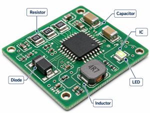
A PCB-mounted inductor stores energy in a magnetic field and resists rapid current change. In switching power supplies, it transfers energy while smoothing current ripple. In signal and power-input networks, it can filter high-frequency noise or form part of a tuned circuit. The reference designator is commonly “L,” but package appearance alone does not identify the electrical function.
The component may contain a wound conductor around a ferrite or powdered-metal core, a molded composite body, or an air-core winding. Its field is not completely confined, even when the part is described as shielded. That remaining leakage field is why the position of an inductor on PCB assemblies, its orientation, and nearby copper still matter.
| Inductor type | Typical application | Selection priorities | PCB design and assembly checks |
|---|---|---|---|
| Shielded power inductor | Buck, boost, and other switching converters where EMI control matters | Inductance, saturation current, RMS current, DCR, core loss, temperature rating | Keep the switch-node path compact; verify thermal rise and the manufacturer’s copper/keepout guidance |
| Unshielded power inductor | Cost-sensitive power conversion where leakage field can be tolerated | Inductance, current ratings, DCR, loss, magnetic-field characteristics | Increase separation from sensors, RF, feedback, and other sensitive circuits; validate EMI |
| Molded SMD power inductor | Compact, high-current converters and automated SMT assembly | DC-bias behavior, saturation, DCR, loss, package stress, reflow rating | Use the recommended land pattern, paste design, placement clearance, and reflow profile |
| Wirewound chip or RF inductor | RF matching, bias networks, filters, and lower-current signal circuits | Q factor, self-resonant frequency, impedance, tolerance, current rating | Control pad and trace parasitics; keep noisy power magnetics and coupling sources away |
| Through-hole or toroidal inductor | High-current filters, energy storage, or designs needing larger magnetic components | Inductance, current, winding insulation, temperature, dimensions, mass | Confirm hole pitch and clearance; add mechanical retention when mass or vibration makes leads insufficient |
How Do You Select the Right Power Inductor for PCB Design?
Select the inductor from the converter’s real electrical and thermal operating range. Selecting an inductor on PCB power stages begins with the regulator data sheet or design tool, followed by verification against the inductor manufacturer’s curves. Input voltage, output voltage, switching frequency, load current, transient requirement, and allowable ripple all influence the required inductance.
- Inductance: Confirm the nominal value and tolerance across the relevant temperature and bias range, not only at the catalog test condition.
- Saturation current: Isat indicates where inductance falls by a stated amount. The definition varies by manufacturer, so compare curves and test conditions.
- RMS current: Irms is normally tied to a specified temperature rise. It is not interchangeable with saturation current.
- DC resistance: DCR creates copper loss proportional to current squared and directly affects efficiency and temperature.
- AC and core loss: Ripple amplitude, frequency, waveform, and flux swing can create substantial loss even when DCR appears acceptable.
- Frequency behavior: SRF and Q matter in RF or filtering applications. Operation too close to self-resonance can invalidate the expected inductive behavior.
- Mechanical envelope: Verify footprint, height, mass, terminal style, and assembly process before approving the MPN.
A shielded power inductor usually contains its field better than an unshielded type, but it may run hotter or have higher DCR. When substituting an inductor on PCB assemblies, compare the Isat definition, loss model, core material, and temperature ratings rather than relying on inductance and package size alone.
How Should a Power Inductor Be Placed in a Buck or DC-DC Converter PCB Layout?
Use the regulator’s reference layout as the first placement authority. When placing an inductor on PCB power stages for a buck converter, keep the input capacitor, switching IC, power inductor, and output capacitor in a compact functional chain. The switch-node connection from the IC to the inductor should be short, and its exposed copper area should be no larger than required for current and heat.
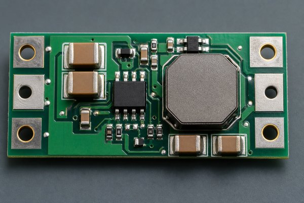
- Start with the input loop: Place the high-frequency input capacitor close to the regulator power and ground pins to minimize the highest di/dt loop.
- Control the switch node: Connect the switching pin to the inductor with a short, direct copper region while avoiding unnecessary spreading.
- Close the output path: Connect the inductor output to the output capacitor with a low-impedance path appropriate for the load current.
- Protect feedback: Route the feedback sense path away from the switch node, inductor, gate-drive traces, and noisy return currents.
- Separate sensitive circuits: Keep clocks, ADC inputs, sensors, high-impedance nodes, and small-signal connectors outside the magnetic and electric noise region.
A power inductor PCB layout example can explain geometry, but it cannot replace the exact IC data sheet. Pinout, grounding, stackup, switching frequency, and control method change the current paths. Copying a visually similar regulator layout can create a larger hot loop or an incorrect feedback return.
How Do Inductor Orientation and Spacing Affect EMI and Magnetic Coupling?
Orientation changes coupling when the inductor’s leakage field is directional. Orientation matters most when adjacent windings can behave like a weak transformer, transferring noise between converters or into a sensitive circuit. The amount depends on core construction, winding axis, current waveform, frequency, distance, and the orientation of both parts.
Rotating one inductor by 90 degrees may reduce coupling for some geometries, but it is not a universal rule. The best orientation for an inductor on PCB layouts depends on whether it is molded, drum-core, toroidal, or air-core. Manufacturer field plots or emission measurements are more reliable than a generic orientation diagram.
- Increase separation: Distance is often the simplest way to reduce magnetic interaction when board area allows.
- Change the field axis: Evaluate orthogonal placement when two directional inductors must remain close.
- Avoid sensitive neighbors: Do not place Hall sensors, magnetometers, high-gain analog circuits, or unshielded cables beside a power inductor without validation.
- Measure the assembly: Check emissions and victim-circuit behavior at the operating currents, modes, and frequencies that create the worst field.
Can Traces, Components or a Ground Plane Go Under an Inductor?
Never apply one universal copper rule beneath every inductor. Copper decisions beneath an inductor require package-specific evidence. Sensitive control traces should generally stay away from the area under a switching inductor, while ordinary traces, components, or a ground plane require a conditional review.
A solid ground plane can provide an electric-field shield and maintain return-path continuity. However, copper beneath an inductor on PCB layers can also create eddy-current loss, alter effective inductance, or change heat flow. Some regulator and inductor manufacturers recommend a ground plane, while others specify a copper keepout under a particular package.
- Follow package guidance: Use the component land-pattern and keepout drawing when it explicitly defines bottom-side copper, vias, or exposed areas.
- Keep signals out: Avoid routing feedback, sensing, clocks, reset lines, and other high-impedance signals beneath the inductor.
- Protect return paths: Do not cut a ground plane in a way that forces nearby high-frequency current around a long discontinuity.
- Validate uncertain cases: Compare temperature, ripple, efficiency, and emissions on prototypes when the reference materials do not give a clear answer.
What Should an Inductor PCB Footprint and Keepout Include?
The manufacturer’s recommended land pattern should control the footprint. A PCB footprint for an inductor cannot rely on body dimensions alone because they do not define terminal geometry, solder fillet, toe allowance, or assembly tolerance. The CAD footprint must match the approved MPN and revision.
- Pad geometry: Check terminal width, pitch, solderable area, mask opening, paste aperture, and allowable overhang.
- Courtyard: Reserve placement, inspection, nozzle, and rework clearance around the maximum component outline.
- Height control: Record the maximum mounted height when the board fits beneath a shield, enclosure, heat spreader, or adjacent module.
- Via strategy: Avoid uncontrolled via-in-pad designs that can wick solder unless the fabrication and assembly process specifically supports filled or capped vias.
- Mechanical support: Provide holes, retainers, or an approved adhesive process for heavy toroidal and large through-hole parts when shock or vibration requires it.
- Keepout definition: Separate electrical copper restrictions from mechanical courtyard and assembly keepout requirements in the design data.
Footprint substitutions deserve special attention. An alternate inductor on PCB assemblies may fit the outline but use different terminal metallurgy, coplanarity, paste coverage, or keepout. Approve it against both circuit requirements and the assembly process.
How Should Heat Be Managed Around a Power Inductor?
Temperature rise must be evaluated at worst-case current and ambient conditions. Thermal analysis must include copper loss from DCR plus core and AC winding losses from switching frequency, ripple, waveform, and core material. Nearby hot components can raise temperature beyond the stand-alone estimate.
Use the manufacturer’s temperature-rise and loss curves when available. Confirm whether the published Irms value is based on a 20°C, 40°C, or another stated rise, and check how the part was mounted during testing. Thermal behavior for an inductor on PCB assemblies can change with copper area, airflow, nearby heat sources, and conformal coating.
- Reduce electrical loss: Select suitable DCR, core material, inductance, and size for the actual ripple and current.
- Manage nearby heat: Avoid clustering the inductor with other hot parts unless the thermal model and measurement support it.
- Preserve airflow: Keep tall components and enclosure walls from blocking the intended cooling path.
- Measure correctly: Use thermal imaging or a validated temperature sensor after the assembly reaches steady operation at worst-case load.
How Are SMD and Through-Hole Inductors Assembled on a PCB?
Assembly must match the package, terminal design, thermal mass, and approved soldering limits. SMD inductors normally use reflow, while through-hole parts may use wave, selective, or controlled manual soldering. The following sequence prevents footprint, soldering, and mechanical-support problems.
- Verify the released component: Match the MPN, value, tolerance, current ratings, package, terminal finish, height, footprint, and assembly drawing before material loading.
- Prepare pads and solder: Confirm pad geometry, solder-mask opening, paste aperture, board finish, cleanliness, and via treatment. Uncontrolled via-in-pad can wick solder away from an SMD terminal.
- Place the component: Control orientation when the drawing identifies pin 1 or a preferred winding direction. Check centering, coplanarity, placement pressure, nozzle clearance, and nearby tall components.
- Apply the correct soldering process: For SMD parts, control ramp rate, peak temperature, and time above liquidus against the component profile. For through-hole parts, ensure adequate barrel fill without overheating the winding, insulation, or core.
- Add mechanical support when required: Heavy through-hole and toroidal inductors may need approved adhesive, a retainer, tie, or nonconductive fastener. The support must tolerate soldering, coating, temperature, shock, and vibration without stressing the leads or forming a shorted turn.
- Inspect before release: Check identity, alignment, solder joints, core damage, residue, retention, clearance, and rework accessibility. Record any manual soldering or adhesive operation required by the build instructions.
Large magnetic parts absorb heat and may show uneven wetting when the profile is too light. Excess paste can cause an SMD part to float or tilt, while insufficient heat can leave weak joints beneath an inductor on PCB assemblies. For broader planning, review the custom PCB assembly services checklist.
How Should PCB-Mounted Inductors Be Inspected and Tested?
Inspection must verify component identity, assembly quality, and electrical performance. No single method can confirm every condition, so the inspection depth should match package visibility, converter risk, production volume, and customer requirements.
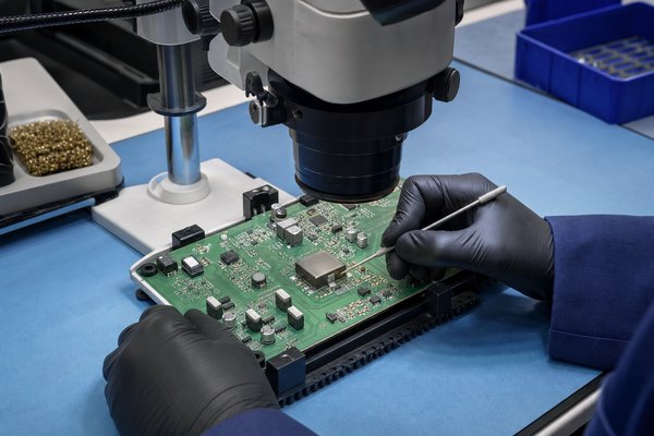
- Identity and orientation: Match the MPN, value, package, reference designator, placement side, and any pin or winding-orientation mark against the BOM and drawing.
- Visual condition: Check offset, tilt, chipped or cracked cores, damaged insulation, contamination, enclosure clearance, and the condition of mechanical retention.
- Solder joints: Look for incomplete wetting, insufficient solder, bridging, lifted terminals, disturbed joints, cracked fillets, and poor through-hole barrel fill. Use X-ray or another suitable method when the terminal is hidden and the risk justifies it.
- Electrical characteristics: Use an LCR meter with the specified frequency, signal level, and fixture compensation when inductance, DCR, Q, or impedance must be verified. Remove or account for parallel circuit paths before interpreting an in-circuit result.
- Functional performance: Measure output regulation, ripple, switching waveform, transient response, peak current, and protection behavior at representative input voltages and loads.
- Thermal, acoustic, and EMI behavior: After temperatures stabilize, check case temperature, hotspots, emissions, and audible noise at full load, transient load, and relevant light-load modes.
- Records and disposition: Link failures, rework, retest, measurements, equipment, lot identity, and final acceptance to the production record when traceability is required.
A multimeter continuity check only screens for an open winding or unusual resistance. Because a healthy power inductor can have very low DCR, it may appear shorted. Testing an inductor on PCB assemblies this way does not confirm inductance under bias, saturation margin, core loss, or converter performance.
What Causes an Inductor on a PCB to Overheat, Buzz or Fail?
Start troubleshooting from the symptom, operating mode, and measured waveform. Record input voltage, load, ambient temperature, switching mode, and the exact inductor MPN. Replacing the part without identifying current, frequency, layout, or assembly causes may only hide the problem.
| Observed symptom | Most likely causes | How to confirm | Recommended action |
|---|---|---|---|
| Overheating | Excess RMS current, saturation at peak current, high DCR, core loss at the actual switching frequency, poor airflow, or heat from nearby parts | Measure current and temperature at worst-case input/load; compare peak and RMS current with the data-sheet curves and estimate copper plus core loss | Select adequate saturation and thermal margin, reduce loss, improve copper/airflow, or move the inductor away from external heat sources |
| Audible buzzing | Magnetostriction, loose windings, pulse-skipping or burst mode, ceramic-capacitor interaction, PCB resonance, or inadequate mechanical support | Compare noise across load and control modes; localize the sound and inspect the component, solder joints, and board support | Use a quieter operating mode or qualified low-noise inductor; correct soldering and add approved retention where required |
| EMI or circuit interference | Large switch-node copper, excessive loop area, unshielded leakage field, poor orientation, or sensitive traces/components placed too close | Use a near-field probe and oscilloscope; compare orientation or spacing changes and review the power-loop and return-path geometry | Shrink the noisy loop and switch node, reroute sensitive signals, increase separation, or use a suitable shielded component |
| Unstable output or current spikes | Inductor saturation, wrong inductance under DC bias, poor feedback routing, unsuitable substitute, or an intermittent solder connection | Capture switch-node and inductor-current waveforms; verify the exact MPN, bias curve, peak current, feedback path, and solder joints | Restore current and inductance margin, correct the layout or BOM, and repair the assembly process rather than only replacing the part |
| Open circuit or physical damage | Cracked termination, lead fatigue, handling impact, vibration, excessive reflow exposure, or insufficient support for a heavy component | Perform visual inspection, continuity/DCR comparison, joint microscopy, and controlled mechanical examination when appropriate | Correct land pattern and soldering, control handling/reflow, and add specified mechanical retention for high-mass inductors |
Inductance often falls as DC bias increases, and it can drop sharply near saturation. For an inductor on PCB power stages, the resulting current rise may increase heating and stress the regulator. That feedback effect is why peak current and the full bias curve matter more than a single zero-bias inductance reading.
What Common Inductor PCB Layout Mistakes Should Be Avoided?
Most layout failures come from applying a valid rule in the wrong electrical context. Review current paths, field exposure, thermal behavior, package guidance, and assembly limits together. Each common mistake below includes the practical way to avoid it.
- Inductor placed too far from the regulator: A long switch-node connection increases parasitic inductance and noise. Avoid it by following the reference placement and keeping the switching connection short and direct.
- Oversized switch-node copper: Excess area increases capacitive coupling and radiated electric field. Avoid it by using only the copper required for current, heat, clearance, and manufacturability.
- Feedback routed through the noisy region: A sense line beside or beneath the inductor can disturb regulation. Avoid it by routing feedback away from the switch node and sensing from the manufacturer-recommended output point.
- Sensitive circuits placed too close: Sensors, clocks, RF paths, high-impedance nodes, and connectors may receive magnetic or electric-field interference. Avoid it by increasing separation, protecting return paths, and validating orientation where space is limited.
- One ground-plane rule used for every package: Automatically adding or removing copper can harm return paths, efficiency, or inductance. Avoid it by following the exact regulator and inductor documentation and measuring unclear cases.
- Current path and vias undersized: Narrow copper or too few vias create voltage drop and localized heating. Avoid it by calculating current capacity, resistance, temperature rise, and layer-transition requirements.
- Alternate parts approved by value alone: Matching only inductance ignores Isat, Irms, DCR, loss, shielding, height, and footprint. Avoid it by defining non-negotiable parameters and requiring engineering approval for substitutions.
- Mechanical support omitted: Heavy components can fatigue leads and solder joints during handling, shipping, or vibration. Avoid it by specifying retention, clearance, and acceptance criteria in the assembly documentation.
High-current paths also require suitable copper width, layer transitions, and via capacity. If the converter carries substantial current, the surrounding board design should be reviewed as a high-current PCB system rather than treating the inductor footprint in isolation.
What Information Is Required for Inductor PCB Assembly?
A production package needs the exact MPN and its non-negotiable parameters. A value such as “10 µH” is insufficient; current ratings, DCR, package, shielding, temperature range, and terminal finish determine whether a substitute is acceptable.
- BOM: Provide manufacturer, complete MPN, quantity, reference designators, and approved-alternate status.
- Electrical limits: State inductance, tolerance, Isat, Irms, DCR, SRF or Q when relevant, and operating temperature.
- Fabrication data: Supply released Gerber or ODB++, drill data, stackup, board outline, and revision.
- Placement data: Supply CPL coordinates, side, rotation, reference designator, and assembly drawing.
- Process notes: Define adhesive, staking, coating exclusions, manual operations, special soldering, and cleaning restrictions.
- Acceptance: Define inspection, functional test, thermal check, traceability, and reporting requirements appropriate to the project.
Before changing an inductor on PCB production builds, obtain design approval for differences in core material, shielding, saturation curve, loss, height, terminal geometry, and soldering profile.
How Do You Review an Inductor PCB Layout Before Production?
The final review should find mismatches before purchasing and assembly begin. Cross-check the schematic, layout, BOM, assembly notes, and verification plan; a revised MPN paired with an obsolete footprint is a common release error.
- Confirm revisions: Match the released schematic, data sheet, MPN, footprint, and board revision.
- Trace the current paths: Review the input loop, switch node, inductor-to-output path, return plane, and layer transitions.
- Review noise exposure: Check feedback, sensing, clock, RF, and analog routes against the inductor field and switching copper.
- Check physical fit: Verify height, courtyard, enclosure, nozzle, rework, fixation, and vibration clearances.
- Control substitutions: Record approved alternates and changes that require renewed approval.
- Plan verification: Define functional, ripple, transient, thermal, audible-noise, and EMI checks for the risk level.
Complete this review before tooling and purchasing are committed. EBest Circuit can review PCB and PCBA release data for manufacturability and quotation; the project owner remains responsible for circuit targets and final validation.
FAQs About Inductor on PCB
Q1: Can another component be placed directly under a power inductor?
A1: Avoid placing sensitive or heat-critical components directly beneath it unless the documentation allows it. Check leakage field, switch-node coupling, temperature, assembly clearance, and rework access on the actual stackup. Validate tight placement under worst-case conditions.
Q2: Should copper or the ground plane be removed under an inductor?
A2: There is no universal rule. A ground plane may preserve the return path and provide electric-field shielding, while copper beneath some packages can increase loss or change inductance. Follow the component and regulator guidance, keep sensitive traces away, and measure uncertain designs.
Q3: How close should the inductor be to the switching regulator?
A3: Keep the switch-node connection short without violating the reference layout or thermal clearance. Prioritize the input capacitor and highest di/dt loop, then place the inductor and output capacitor so the power path remains compact and feedback stays quiet.
Q4: Does rotating nearby inductors by 90 degrees reduce coupling?
A4: It can help when leakage fields are directional, but it is not guaranteed. Core shape, shielding, winding axis, waveform, frequency, distance, and both orientations affect coupling. Confirm the result with field information or measurements.
Q5: How should a heavy toroidal inductor be fixed to the PCB?
A5: Match mechanical support to mass, vibration, temperature, and service conditions. Options include approved adhesive, a nonconductive retainer, tie, or center fastener. Avoid conductive hardware that could act as a shorted turn, and do not rely on leads alone under significant load.
Q6: How is the lead pitch determined for a custom toroidal inductor footprint?
A6: Base the pitch on the finished winding, not only the bare core. Account for lead direction, bend radius, insulation clearance, assembly tolerance, and retention. Measure representative samples before freezing the footprint.
Q7: Can a power inductor interfere with an SD card, sensor, or analog circuit?
A7: Yes, especially near magnetic, high-impedance, analog, or high-speed circuits. Leakage magnetic field and switching-node electric field can couple into them. Increase separation, protect return paths, consider orientation and shielding, and test at worst-case load.
Q8: Should the output capacitor connect directly to the inductor pad?
A8: Keep the connection short and low impedance, following the regulator reference layout. Preserve the intended current flow, ground return, and feedback-sense point. Avoid a long narrow trace or sensing from a noisy, heavily loaded location.
Q9: Can signal traces be routed beneath a switching inductor?
A9: Keep feedback, sensing, clock, reset, RF, and other sensitive traces away. Less-sensitive routing still requires review against the package keepout, stackup, return path, and manufacturer guidance. An electrically functional trace may still create noise or test-access problems.
Q10: Why can a buck converter work but still show poor regulation or EMI?
A10: Correct average output voltage does not prove that the layout is robust. A large hot loop, oversized switch node, weak capacitor path, noisy feedback, saturation, or poor grounding can remain hidden. Check ripple, transients, current waveform, temperature, and emissions.
Conclusion
A reliable inductor design closes the loop from selection to measured assembly performance. Use component and regulator documentation to establish ratings and layout, then verify footprint, copper strategy, heat, soldering, mechanical support, ripple, and EMI under realistic conditions. No single placement or ground-plane rule applies to every package.
For a manufacturability review and quotation, send your Gerber/ODB++, BOM, CPL, assembly drawing, quantity, test requirements, and inductor specifications to sales@bestpcbs.com. A complete package helps identify footprint, sourcing, assembly, and verification risks before production begins. Revisit this Inductor on PCB checklist whenever the regulator, stackup, enclosure, or approved MPN changes.