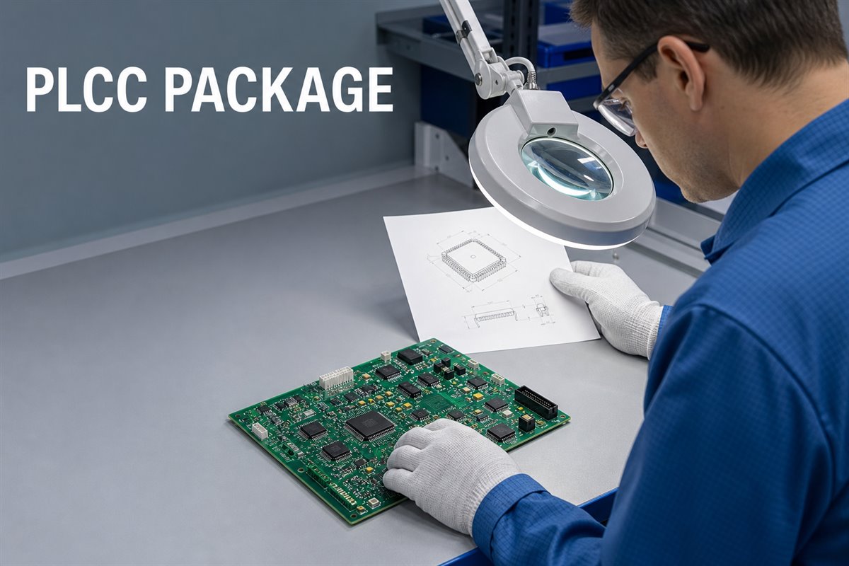
A PLCC package is a plastic leaded chip carrier with J-shaped leads folded under the package body. It can be mounted in a socket or soldered directly to a printed circuit board. That flexibility made PLCC devices common in memory, controllers, processors, programmable logic, and many long-life industrial products.
For a PCB assembly buyer, however, recognizing the package name is only the beginning. The exact manufacturer part number, pin count, body dimensions, land pattern, Pin 1 orientation, component supply condition, soldering process, and inspection method must all agree. A PLCC component that looks correct can still be the wrong ordering code or a poor match for the released footprint.
This guide explains the package from a PCB and PCBA manufacturing perspective. It shows what engineers and buyers should confirm before component sourcing, stencil release, assembly, inspection, rework, and repeat production.
What Is a PLCC Package?
PLCC means plastic leaded chip carrier. The package usually has leads on four sides, with each lead curling inward beneath the molded body in a J shape. Unlike a leadless chip carrier, a PLCC has formed metal leads. Unlike a typical QFP, its leads do not extend outward as long gull-wing terminals.
Many PLCC families use a 1.27 mm lead pitch, but the package name alone does not establish the complete mechanical specification. Different devices can have different pin counts, body sizes, heights, tolerances, ordering codes, moisture-handling requirements, and manufacturer-recommended footprints. The current component datasheet and package drawing must control the build.
PLCC devices may be directly soldered to the PCB or installed in a matching socket. A socket makes component removal or replacement easier, but it also adds height, cost, contacts, and another mechanical interface. Direct soldering creates a lower-profile assembly but makes replacement more dependent on controlled rework.
If an incoming part must be identified from its body markings, use the marking, BOM, manufacturer documentation, package dimensions, and board records together. The PCB components identification guide explains why one visible code is not enough to approve a component for production.
How Does a PLCC Package Connect to a PCB?
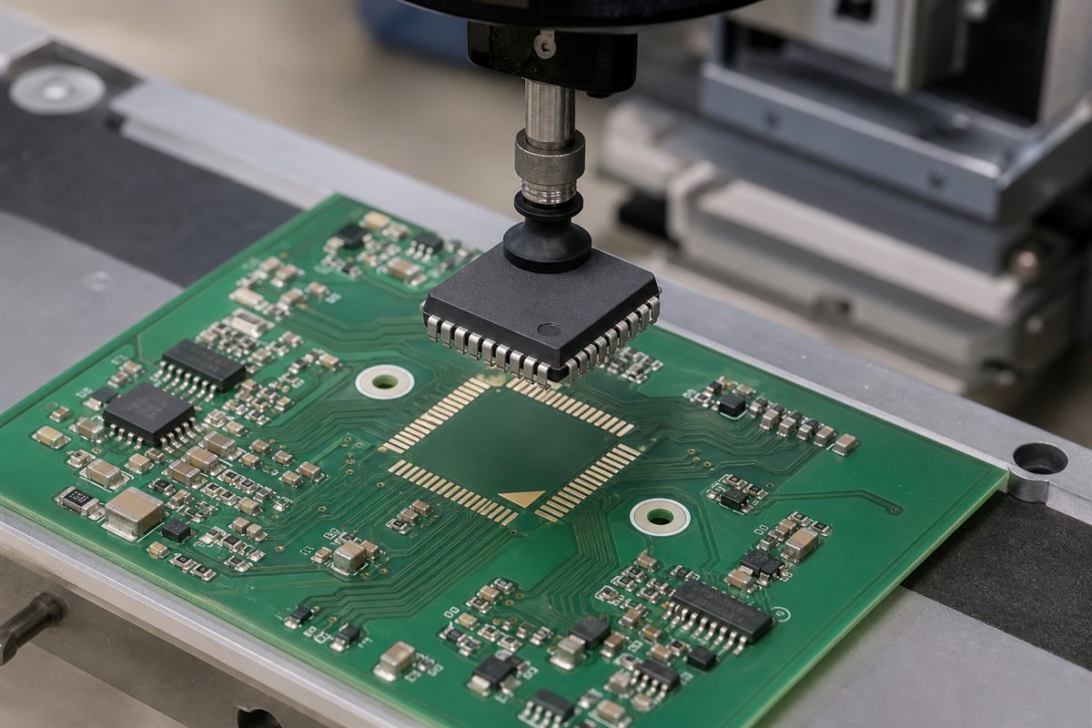
A directly soldered PLCC sits over perimeter pads on the PCB. Solder paste is printed on the lands, the component is placed with the correct orientation, and the assembly passes through the approved reflow process. The solder joints form around the exposed lower portions of the J-leads.
The inward lead shape saves board area, but it also changes what can be seen after soldering. Part of each termination is close to or under the package body. This means a board can look generally acceptable from above while still requiring closer inspection of lead wetting, alignment, bridging, insufficient solder, or lifted leads.
A socketed build follows a different path. The PCB is assembled with the PLCC socket, and the IC is inserted later. The socket footprint, socket orientation, insertion method, retention, overall height, and access for removal all become part of the assembly review.
Before choosing the mounting method, confirm:
- whether the released BOM calls for the IC alone or an IC-and-socket combination;
- whether field replacement or programming access requires a removable device;
- whether the enclosure allows the added socket height;
- whether vibration, contact resistance, thermal cycling, or handling affects the product requirement;
- whether the production quantity and test flow support manual insertion after reflow.
The customer’s product team remains responsible for the electrical and system-level choice. EBest Circuit (Best Technology) can review the released PCB, BOM, CPL, assembly drawing, and process notes for manufacturing conflicts before PCBA production.
PLCC Package Sizes, Pin Counts, and Footprints
PLCC is a package family, not one universal outline. Common devices include square and rectangular bodies with different pin counts. Manufacturer drawings also define body dimensions, lead pitch, lead width, seating details, tolerances, and the Pin 1 index area.
The risk appears when a BOM uses only a generic description such as “PLCC-44” while the PCB library was created from a different device or socket drawing. The pin count may match, but the body, lead geometry, courtyard, socket requirements, or recommended land pattern may not.
Use this identification chain before approving the footprint:
- complete manufacturer part number and ordering code;
- manufacturer and current datasheet revision;
- package name, pin count, pitch, and drawing code;
- body width, body length, and maximum seated height;
- terminal dimensions and recommended PCB land pattern;
- Pin 1 marking and pin-numbering direction;
- tube, tray, tape, or other delivery format needed for assembly.
For example, Microchip publishes separate PLCC package outline drawings, while NXP lists package-specific dimensions and mounting details for PLCC families. These sources illustrate why a generic package label should never replace the exact component drawing.
The existing guide to part number width specifications provides a broader method for reconciling ordering codes, package drawings, tolerances, land patterns, and incoming parts.
Socketed vs Soldered PLCC Assembly
| Decision | Socketed PLCC | Directly soldered PLCC |
| Replacement | Easier device removal | Requires controlled rework |
| Assembly height | Higher | Lower |
| Interfaces | Socket plus IC contacts | Solder joints to PCB |
| Production steps | Socket assembly and IC insertion | Placement and reflow |
A socket is useful when the component must be removed for programming, service, configuration, or replacement. It can also protect the IC from the primary soldering process when the released product plan requires later insertion.
But a socket is not automatically the safer manufacturing option. A mismatched socket, reversed socket, bent contact, incomplete insertion, or excessive insertion force can stop the board at test. Added height may also interfere with an enclosure or neighboring hardware.
Direct soldering eliminates the socket interface and supports automated SMT assembly. The process must still match the component’s approved storage, handling, placement, and reflow requirements. Old or separately sourced PLCC stock should not be released to the line only because the part number appears correct.
For repeat builds, record the approved part, socket if used, footprint revision, orientation image, insertion step, inspection criteria, and any programming sequence. These records reduce the risk of the next lot being built from an incomplete purchasing description.
How Should a PLCC Footprint Be Reviewed?
A footprint review does not redesign the circuit. It compares the released component data with the PCB land pattern and the needs of fabrication, assembly, inspection, and rework.
Key review points include:
- Land geometry. Compare pad length, width, pitch, and location with the current manufacturer recommendation or the customer-approved library standard.
- Pin 1 control. The PCB, silkscreen, assembly drawing, CPL rotation, and component marking must communicate the same orientation.
- Solder mask and paste. Openings must support the released pad and stencil strategy without creating avoidable bridging or insufficient solder risk.
- Courtyard and access. Nearby components, sockets, connectors, enclosure parts, and rework tools need adequate clearance.
- Board support. Large packages and sockets should not sit in areas where panel handling, depaneling, or board flex creates unnecessary mechanical stress.
- Inspection visibility. The layout should allow the planned inspection method to view the relevant lead areas.
A common failure scenario is a correct IC placed on a footprint copied from an unrelated PLCC library entry. The board reaches SMT, but the land geometry or orientation convention does not match the released part. Production then stops for engineering clarification, stencil revision, PCB rework, or a new board revision.
Sending the exact package drawing with the Gerber or ODB++, BOM, CPL, and assembly drawing lets the PCBA supplier raise this conflict before materials and schedules are committed.
Common PLCC Soldering and Assembly Problems
PLCC assembly problems are usually not caused by the package name itself. They come from mismatched data, uncontrolled materials, or a process that does not account for the J-lead geometry.
Wrong orientation. If the CPL rotation, silkscreen mark, drawing, and package index are inconsistent, a correctly sourced component can be placed 90 or 180 degrees from the intended orientation. Clear Pin 1 documentation and first-article confirmation reduce this risk.
Solder bridging. Excess paste, poor alignment, inappropriate stencil openings, contamination, or lead damage can connect adjacent terminations. The consequence may be an immediate electrical short or a board that fails powered testing.
Insufficient solder or poor wetting. Storage condition, surface contamination, lead finish, paste transfer, land geometry, or reflow conditions can leave a weak or incomplete joint. A simple top view may not show the full condition around the J-lead.
Lifted or damaged leads. Improper handling, unsuitable packaging, or uncontrolled rework can deform a lead. The component may still sit on the board while one termination does not contact the land correctly.
Package-to-footprint mismatch. A buyer approves an alternate with the same function and pin count, but the package drawing is different. This can cause placement, soldering, clearance, or inspection problems even before electrical compatibility is considered.
Uncontrolled legacy stock. A part may be obsolete, aged, repacked, or supplied without enough traceability and handling information. The sourcing decision should be completed before the SMT schedule is fixed. See the BestPCBS component sourcing resources for the BOM information buyers should prepare.
How Are PLCC Solder Joints Inspected?
Inspection should answer a defined risk question. It should not be added as a generic line in the quotation without clear coverage.
Visual inspection can check orientation, body damage, obvious offset, exposed lead condition, and visible solder quality. AOI can support repeatable checks for placement, polarity, bridging, and other visible conditions when the package and board geometry provide a usable camera view.
However, AOI cannot prove component function, and the inward J-lead shape limits visibility compared with a long outward gull-wing lead. If the acceptance requirement depends on an area that is not adequately visible, the customer and supplier should agree on another suitable method rather than claiming that AOI proves every joint.
Electrical or functional testing addresses a different question: whether the assembled board behaves according to the customer’s defined test plan. Testing requires suitable test points, firmware or programming files when applicable, fixtures or connection instructions, limits, and pass/fail criteria.
The AOI in PCB manufacturing guide explains how AOI differs from SPI, X-ray, electrical checks, and functional testing.

PLCC vs QFP and BGA Packages
| Package | Connection style | Manufacturing consideration |
| PLCC | J-leads under body edge | Socket option and partial joint visibility |
| QFP | Gull-wing leads extend outward | Lead coplanarity and fine-pitch handling |
| BGA | Solder balls under package | Hidden joints and X-ray planning |
PLCC, QFP, and BGA describe different mechanical connection systems. They should not be treated as interchangeable simply because two devices offer similar electronic functions.
A QFP usually provides more visible solder joints, but its outward leads increase the package footprint and can be vulnerable to handling damage. A BGA supports a high connection count beneath the body, but its joints are hidden and require a different land pattern, stencil strategy, reflow process, and inspection plan.
The package choice belongs to the customer’s electronic and product design team. From the manufacturing side, the important task is to build the released package correctly and identify when the BOM, footprint, placement data, inspection access, and replacement plan do not agree.
What Should You Send for a PLCC PCBA Quote?
A quotation based only on board size, layer count, and the phrase “PLCC assembly” leaves too many assumptions open. A useful RFQ connects the component, PCB, assembly process, inspection, testing, and delivery requirement.
Send these files and decisions:
- Gerber or ODB++ files, NC drill data, and fabrication drawing;
- complete BOM with exact manufacturer part numbers and approved alternates;
- CPL or centroid file with designators, coordinates, side, and rotation;
- assembly drawing with Pin 1, polarity, no-fit, and special handling notes;
- PLCC manufacturer datasheet and package drawing;
- socket manufacturer part number and insertion instructions, if applicable;
- customer-supplied versus supplier-sourced component responsibility;
- inspection, programming, functional test, acceptance, and packing requirements;
- prototype and production quantities plus the requested delivery schedule.
A realistic production example. A buyer requests 100 controller PCBAs using a legacy 44-lead PLCC. The BOM lists a shortened part number, while the PCB library name only says “PLCC44.” One supplier quotes immediately. Another supplier asks for the complete ordering code and package drawing, then finds that the proposed substitute and the released land pattern do not share the same approved mechanical details.
The second supplier has not redesigned the product. It has prevented an unapproved assumption from reaching purchasing and SMT. The buyer can now confirm the exact component, approve a documented alternate, or revise the released footprint before ordering boards and material.
When delivery is urgent, the same principle applies. The fast PCB assembly guide explains why BOM and DFM review should happen before an accelerated schedule is promised.
EBest Circuit (Best Technology) can support PCB manufacturability review, PCB fabrication, BOM sourcing, SMT and mixed PCBA, inspection, and testing assistance based on customer-provided specifications. Send the files above to sales@bestpcbs.com for a quotation review.
FAQs About PLCC Packages
What does PLCC mean?
PLCC means plastic leaded chip carrier. It is an IC package family commonly identified by J-shaped leads along the package sides.
Can a PLCC package be soldered directly to a PCB?
Yes. Many PLCC devices can be directly soldered to an approved PCB land pattern. The exact component datasheet, footprint, handling, and assembly requirements must be followed.
Can every PLCC device use a socket?
No. The device pin count, outline, socket specification, orientation, height, and product requirements must match. A generic PLCC description does not prove socket compatibility.
Is a PLCC footprint determined only by pin count?
No. Pin count is only one identifier. Confirm the complete ordering code, pitch, body dimensions, terminal geometry, package drawing, recommended land pattern, and Pin 1 convention.
Can EBest Circuit help assemble boards with PLCC components?
Yes, when the released PCB and assembly package is complete. EBest Circuit can support manufacturability review, PCB fabrication, BOM sourcing, PCBA, inspection, and agreed testing assistance. The customer remains responsible for component selection and electrical design approval.
If your next PLCC package project needs PCB fabrication, component sourcing, assembly review, inspection planning, or a build quotation, send your Gerber or ODB++ files, BOM, CPL, package drawing, quantities, and test requirements to sales@bestpcbs.com.