A motion sensor PCB can pass electrical testing yet still produce false triggers, unstable readings, or inaccurate detection results. Electrical interference, sensor placement, and assembly stress are common sources of problems that basic PCB testing may not reveal.
Whether you’re developing a PIR motion sensor light, a MEMS motion tracking device, or a wireless detector, you need a manufacturer that can handle the PCB fabrication, sensor assembly, and testing requirements of your design. Understanding these requirements early can help you avoid production delays, unexpected costs, and reliability problems.
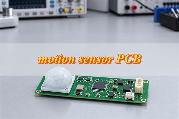
Are you worried about your motion sensor PCB project?
- False triggers after assembly: Noise, mounting stress, unstable power, or enclosure effects can change sensor behavior even when basic electrical checks pass.
- Unclear test coverage: AOI and continuity testing cannot prove detection range, sensor orientation, firmware behavior, or wireless performance.
- Cost and schedule surprises: Sensor availability, fine-pitch assembly, programming, fixtures, and calibration can change the quotation and lead time.
Which Type of Motion Sensor PCB Is Right for Your Application?
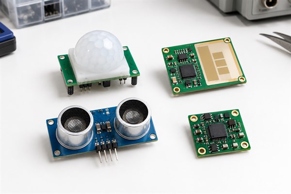
Choosing the right motion sensor PCB starts with what your product needs to detect. PIR, microwave, ultrasonic, and MEMS sensors work differently, and each places different demands on the PCB.
| Motion Sensor PCB Type | Applications | Key PCB Requirements |
|---|---|---|
| PIR Motion Sensor PCB | Motion sensor lights, security alarms | Low-noise analog circuits, stable power, optical alignment |
| Microwave Motion Sensor PCB | Smart lighting, automatic doors | RF layout, antenna clearance, grounding |
| Ultrasonic Motion Sensor PCB | Proximity detection, automated equipment | Transducer connections, driver circuits |
| MEMS Motion Sensor PCB | Wearables, robotics, sports monitoring | Compact SMT assembly, sensor orientation, mechanical stability |
Wireless communication can be added to any of these systems using Bluetooth Low Energy, Wi-Fi, or another suitable radio technology. The sensing method and communication interface should be selected independently to match the intended application.
What Should You Consider Before Designing a Custom Motion Sensor PCB?
A custom motion sensor PCB needs to meet the product’s detection, electrical, mechanical, and assembly requirements. Addressing the following factors during design can prevent problems that become expensive to correct after production begins.
- Detection Requirements: For PIR applications, establish the detection range, coverage angle, response time, and acceptable false-trigger behavior. MEMS applications require defined measurement ranges, sensing axes, sampling rates, and accuracy targets. These specifications help determine the sensor IC and supporting circuitry.
- PCB Structure and Component Placement: Select the layer count, board dimensions, thickness, and mounting locations to suit the enclosure. Keep MEMS sensors away from areas subject to excessive bending or mounting stress. PIR sensors also need proper alignment with the optical lens and intended detection field.
- Power Management: Battery-powered motion sensors need low standby current and stable voltage regulation. Wireless devices may draw brief current peaks during transmission, so the power distribution and decoupling must prevent these changes from disturbing sensitive sensor circuits.
- RF and Antenna Layout: Microwave sensors and wireless modules need suitable antenna clearance, grounding, and RF routing. Batteries, metal enclosures, and nearby copper can affect antenna performance. Follow the module manufacturer’s reference layout and check the antenna arrangement in the finished product.
- Sensor Package Compatibility: Check component footprints, soldering limits, moisture sensitivity, and availability before finalizing the BOM. MEMS devices in LGA packages may need specific land patterns, stencil openings, and reflow conditions to avoid poor solder joints or excessive package stress.
- Programming and Test Access: Include accessible points for power measurements, programming, communication signals, and relevant sensor outputs. Without adequate test access, production may require more complex fixtures, increasing test time and cost.
A design that accounts for these requirements is easier to manufacture, assemble, and verify without unnecessary revisions.
How Can You Reduce Signal Noise and False Triggers in a Motion Sensor PCB?
Reducing signal noise starts with the PCB layout, power supply, sensor mounting, and signal-processing circuit. The causes of unstable readings vary between PIR, MEMS, and microwave sensors, so the solution must match the problem.
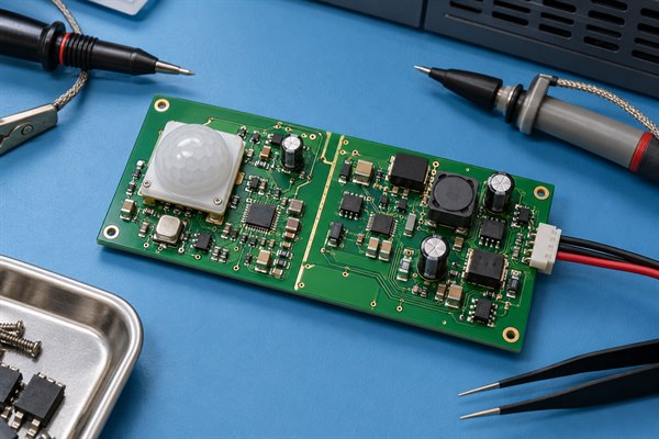
- Minimize Interference in PIR Circuits: PIR sensors generate weak signals that can be affected by nearby electrical noise. Keep sensitive analog traces away from switching regulators, relay drivers, and high-current paths. Proper grounding, local decoupling, and signal filtering help reduce interference at the sensor input.
- Optimize Signal Amplification and Filtering: Increasing amplifier gain also increases unwanted noise. Choose gain, bandwidth, and detection thresholds that suit the expected motion signal. Test the complete signal chain to confirm that the required sensitivity is maintained without excessive false triggering.
- Reduce Mechanical Stress on MEMS Sensors: PCB bending, mounting pressure, and soldering stress can change accelerometer or gyroscope readings. Follow the sensor manufacturer’s footprint and reflow recommendations, support the PCB during assembly, and avoid placing sensitive devices in areas of concentrated strain.
- Maintain Stable Power and Temperature Conditions: Voltage fluctuations during wireless transmission or output switching can disturb sensor operation. Use appropriate regulation and decoupling, and keep significant heat sources away from temperature-sensitive sensors. Check performance across the intended voltage and temperature range.
- Improve RF Layout and Antenna Performance: Microwave sensors and wireless modules require suitable antenna clearance, grounding, and routing. Metal components, batteries, and enclosure materials can influence RF behavior. Verify the antenna arrangement using the actual product enclosure rather than relying on PCB-level testing alone.
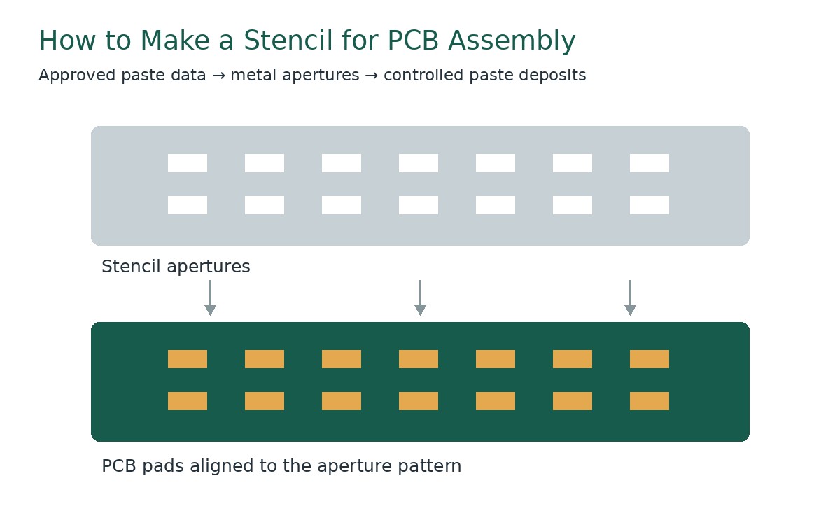
- Control SMT Assembly Quality: Component misalignment, uneven solder joints, and unsuitable reflow conditions can introduce electrical or mechanical problems. Controlled solder paste printing, component placement, and reflow processes help limit these defects. MEMS packages should be handled according to their specific assembly requirements.
- Test Under Real Operating Conditions: Evaluate PIR devices for unwanted triggers related to temperature changes, airflow, and environmental movement. For MEMS products, check measurement stability under expected vibration and mounting conditions. Wireless devices should also be tested during radio transmission and changes in power demand.
PCB manufacturing and assembly controls address many sources of interference and measurement error. Firmware settings, calibration, optical design, and environmental conditions must also be considered when evaluating the finished product.
What Does a Custom Motion Sensor PCB Manufacturing & Assembly Service Include?
EBest Circuit provides PCB fabrication, component sourcing, SMT/THT assembly, inspection, and testing services for custom motion sensor PCB projects. Full-turnkey, partial-turnkey, and consigned assembly options allow customers to select the manufacturing scope that fits their needs.
- Free DFM & Engineering Review: Review Gerber files, PCB stackup, component footprints, BOM, and assembly drawings before fabrication. Identify potential problems involving sensor placement, solder pads, clearances, and manufacturability.
- Custom PCB Fabrication: Manufacture single-sided, double-sided, multilayer, and HDI PCBs using materials, copper thicknesses, and surface finishes suited to the approved design. Standard FR4 construction and finer routing processes are available for different circuit requirements.
- Component Sourcing: Source approved PIR sensors, MEMS devices, microcontrollers, wireless modules, connectors, and passive components. Check availability and confirm any proposed substitutes with the customer before purchasing.
- Precision SMT & THT Assembly: Support single-sided and double-sided SMT, fine-pitch QFN, LGA, BGA, and miniature SMD packages, as well as through-hole and mixed-technology assemblies. Solder paste printing, placement, and reflow conditions are selected to suit the component requirements.
- Quality Inspection & Functional Testing: Provide SPI, AOI, X-ray inspection, and electrical testing where applicable. Firmware programming, sensor output verification, and application-specific functional testing can be arranged when the necessary procedures and fixtures are available.
- Prototype to Mass Production: Support initial prototypes, pilot builds, and volume orders using approved design revisions and BOMs. Production schedules and quality requirements are confirmed against the components and manufacturing processes involved.
How Can You Verify Motion Sensor PCB Quality and Detection Performance?
A motion sensor PCB needs both manufacturing inspection and functional testing. A board may pass electrical continuity checks and assembly inspection without meeting its sensing requirements.
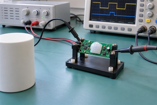
The following tests address different aspects of PCB and PCBA quality:
- PCB Electrical Testing: Check bare boards for open circuits, short circuits, and incorrect connections before assembly. This confirms the required electrical connections but does not establish sensor functionality.
- SMT Assembly Inspection: Use SPI to check solder paste deposits and AOI to identify visible placement errors, polarity problems, and soldering defects. X-ray inspection can examine selected hidden solder joints beneath LGA, QFN, and BGA packages.
- Power Supply and Current Testing: Measure supply voltages, startup behavior, standby current, and active current. Battery-powered wireless sensors should also be checked during sensing and radio transmission, when current demand may change significantly.
- PIR Motion Sensor Testing: Verify sensor response, switching output, and response time under defined conditions. Specify the target, detection distance, movement, sensor orientation, and lens configuration so the results can be reproduced.
- MEMS Motion Sensor Testing: Check I2C or SPI communication, sensing-axis orientation, output data, and stationary offset. Applications requiring higher measurement accuracy may need calibrated equipment to verify sensitivity and response against approved tolerances.
- Microwave Motion Sensor Testing: Check detection response, output switching, and current consumption. Detection coverage and sensitivity should be evaluated with the intended antenna arrangement and enclosure.
- Wireless Communication Testing: Verify the required Bluetooth, Wi-Fi, or other wireless interface, including device connection and sensor data transmission. Communication range and RF performance require separately defined tests when applicable.
- Functional Acceptance and Quality Records: Agree on test conditions, measurable pass/fail limits, firmware versions, and required inspection records. Specify whether each test applies to every board or an approved sample quantity.
EBest Circuit can support project-specific PCBA testing based on the agreed requirements. Sensor calibration, controlled detection-range testing, environmental validation, and complete-device testing should be confirmed before production, as these services may require dedicated equipment or fixtures.
What Affects Custom Motion Sensor PCB Manufacturing Cost and Lead Time?
Motion sensor PCB cost and lead time depend on the board construction, sensor availability, assembly complexity, testing requirements, and order volume. Understanding these factors helps buyers compare quotations and avoid unexpected production delays.
- PCB Construction: Additional layers, fine routing, special materials, and irregular board shapes can increase fabrication complexity. Standard FR4 processes are generally more economical when they satisfy the electrical and mechanical requirements.
- Sensor Availability: Specialized MEMS devices, restricted part numbers, and limited component stock can extend procurement time. Confirm critical sensor availability before releasing the BOM for production.
- Assembly Complexity: Fine-pitch packages, double-sided SMT, and special component handling affect setup and processing time. Some sensors also need additional controls during soldering and inspection.
- Testing Requirements: Firmware programming, calibration, dedicated fixtures, and extended functional tests add work beyond routine assembly inspection. These requirements should be defined before quotation.
- PCB Panelization: Board dimensions, cutouts, and depaneling methods influence material usage and handling. Suitable panelization can improve production efficiency without compromising the board’s mechanical requirements.
- Order Quantity: Prototype and volume orders have different setup, purchasing, and scheduling needs. A pilot build may be appropriate when moving from manually assembled prototypes to automated production.
- Design and BOM Changes: Late revisions can require new stencils, updated placement programs, additional component purchasing, or changes to the test procedure. Finalizing the approved files early helps avoid these delays.
A conventional PIR motion sensor light PCB may have a simpler assembly and test scope than a compact wireless MEMS board with fine-pitch components and calibration requirements. A useful quotation should reflect the complete fabrication, sourcing, assembly, and testing scope rather than the bare-board cost alone.
Motion Sensor PCB Case Study: Dual-PIR Detection for False-Trigger Reduction
Texas Instruments’ TIDA-01069 reference design shows how two PIR sensors and low-power signal processing can be used to reduce unwanted motion detections.
This is a Texas Instruments engineering reference design, not an EBest Circuit customer manufacturing project.
Project Background
The system uses two PIR sensors covering separate detection areas. Powered by a single AAA alkaline battery, it targets low-power applications where false triggering can lead to unwanted alarms or device activation.
Requirements and Challenges
The circuit must acquire weak PIR signals while controlling electrical noise and power consumption. Both sensor channels need suitable positioning, signal conditioning, and dependable data acquisition.
Engineering Solutions
The design combines two PIR sensors, low-power analog circuitry, and signal acquisition. Its implementation highlights several important PCB requirements:
- Accurate placement and orientation of both PIR sensors.
- Low-noise analog routing and appropriate signal filtering.
- Stable power distribution for battery-powered operation.
- Reliable component connections and assembly quality.
- Functional verification of both detection channels.
Documented Results
Texas Instruments reports detection sensitivity exceeding 30 feet (approximately 9 meters) under the reference design’s specified test conditions.
The dual-sensor architecture is intended to help distinguish motion events and reduce unwanted triggering. Actual performance depends on the completed design, assembly, and operating environment.
A similar PCB assembly would require its own manufacturing inspection and functional acceptance tests. The reference design’s results do not establish another manufacturer’s production yield or detection performance.
Why Choose EBest Circuit for Motion Sensor PCB Manufacturing & Assembly?
EBest Circuit brings PCB fabrication, component sourcing, SMT/THT assembly, and engineering support together for custom motion sensor PCB projects. Customers can coordinate these services through one manufacturing supplier.
- Free DFM Review: Receive engineering feedback on PCB construction, footprints, assembly clearances, and potential manufacturing difficulties before production.
- One-Stop PCB and PCBA Services: Arrange PCB fabrication, component procurement, assembly, inspection, and agreed testing through a coordinated manufacturing process.
- Engineering Support: Discuss fine-pitch packages, compact board layouts, sensor mounting conditions, and special assembly requirements with the engineering team.
- Quality Management: EBest Circuit’s public company materials list ISO 9001, ISO 13485, IATF 16949, and AS9100D. Request current certificate copies and confirm the certified site and scope that apply to your order during supplier qualification.
- Prototype and Volume Manufacturing: Move from initial builds to pilot orders and repeat production using approved design files, BOMs, and manufacturing requirements.
- Testing and Traceability Support: Define the required inspection methods, functional tests, component records, and production documentation before manufacturing begins.
- Component Sourcing Assistance: Check availability of critical sensors and coordinate customer-approved alternatives when sourcing constraints arise.
- Delivery Coordination: Establish production and shipment schedules based on the approved order, component readiness, and required manufacturing processes.
EBest Circuit can review your motion sensor PCB design files and provide a manufacturing and assembly proposal based on the board specifications and project requirements.
FAQs About Custom Motion Sensor PCB Manufacturing & Assembly
Q1: Can I supply my own PIR or MEMS sensors for assembly?
A1: Yes. Customer-supplied components can be considered for partial-turnkey or consigned assembly. Packaging, quantity, part identification, and handling instructions should be confirmed before production.
Q2: Can I order bare motion sensor PCBs without assembly?
A2: Yes. Bare PCB fabrication and complete PCBA assembly are available as separate services.
Q3: Is lead-free soldering available for motion sensor PCB assembly?
A3: Yes, provided the selected components and PCB materials are compatible with the approved lead-free soldering process.
Q4: How are moisture-sensitive MEMS components handled?
A4: Handling follows the component’s moisture sensitivity level, storage requirements, allowable exposure time, and manufacturer instructions.
Q5: Can conformal coating be applied to motion sensor PCBs?
A5: Selective coating may be available after reviewing the component restrictions and masking requirements. Sensor openings, connectors, and coating-sensitive parts must be protected.
Q6: Can assembled motion sensor PCBs be delivered without enclosures?
A6: Yes. Completed PCB assemblies can be supplied separately from lenses, housings, and other mechanical components.
Q7: Can PCB fabrication and assembly be quoted separately?
A7: Yes. Quotations can separate PCB fabrication, component sourcing, assembly, and additional testing according to the requested scope.
How Can You Get a Custom Motion Sensor PCB Quote?
EBest Circuit provides custom motion sensor PCB manufacturing and assembly services for prototypes, pilot runs, and volume orders. Send your Gerber files, BOM, pick-and-place data, assembly drawings, quantity, required delivery date, and delivery location. Include the sensor model, firmware files, and functional test specifications where applicable. Contact sales@bestpcbs.com for a free DFM review, manufacturing feasibility assessment, and quotation.