Component misalignment in SMT assembly can come from incorrect placement data, an off-center solder paste deposit, a pick-and-place fault, movement during board transfer, or unbalanced forces in reflow. The fastest way to find the cause is to identify the first point at which the component changes position.
Compare the programmed target, solder paste deposit, as-placed component, position before reflow, and position after reflow in that order. This tells you whether the component was aimed at the wrong location, placed incorrectly, disturbed during transfer, or moved within the reflow process.
What Does Component Misalignment Look Like in SMT Assembly?
Component misalignment is an X, Y, or rotational position error relative to the intended land pattern. It may appear as a sideways shift, end-to-end offset, angular rotation, uneven terminal-to-pad overlap, or a component sitting partly outside its pads.
The same visible offset does not create the same risk for every package. A chip resistor may have uneven overlap at its two ends, while a fine-pitch IC may bring one lead row too close to neighboring pads. Acceptance must therefore consider package geometry, solder-joint condition, electrical clearance, and the applicable customer or workmanship requirement.
Keep these defects separate during diagnosis:
- Wrong polarity: The component is at the correct location, but its positive, negative, or pin-1 orientation is wrong.
- Wrong component: The location is correct, but the installed part number or value is not.
- Tombstoning or billboarding: One end or side has lifted from the board rather than remaining flat and shifting in X, Y, or rotation.
- Missing component: No part is present, which points to pickup, loss, or placement omission rather than positional error.
How Can You Quickly Find Where the Misalignment Started?
Follow one affected reference designator through the process and stop at the first inspection point where its position is wrong. That point directs the investigation to the responsible stage instead of the final stage where the defect happened to be detected.
Step 1: Check the intended placement position. Verify the X/Y coordinates, rotation, board origin, side transform, and package center. The expected position should match the assembly data before any machine setting is changed.
Step 2: Check PCB registration. Review the selected global and local fiducials, panel mapping, and recognition result. A common offset across many components points back to registration or program setup.
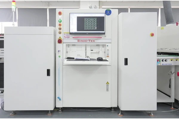
Step 3: Check the solder paste with SPI. Compare deposit position, height, area, and volume on both sides of the affected component. Any offset or imbalance already present here belongs to the printing stage.
Step 4: Check the as-placed component. Review the feeder, nozzle, pickup image, vision result, and component position immediately after release. If it is already off center, the fault is in placement or an earlier stage.
Step 5: Check whether the part moved before reflow. Compare its position at placement exit and near the oven entrance. A difference confirms movement during conveyance, handling, or board flex.
Step 6: Check whether the part moved during reflow. Compare the verified oven-entry position with post-reflow AOI or X-ray data. Movement that first appears across the reflow process points to wetting, thermal, warpage, airflow, or vibration effects.
Make the first correction at the stage where the offset first appears, then repeat that same comparison. Final AOI confirms the finished assembly, but it cannot by itself show which stage created the problem.
Which Misalignment Patterns Point to Different Causes?
The way the error repeats helps you decide what to check first. Treat the pattern as a starting clue, then confirm it by comparing positions before and after the suspected stage.
| What You See | Check First | Likely Cause Area |
| Most components shift in the same direction | Fiducials and placement coordinates | Program setup or board registration |
| One package or reference designator repeatedly shifts | Package center, feeder, nozzle, and vision data | Component data or pick-and-place |
| One PCB area repeatedly shows offsets | SPI results, local board height, and support | Printing, warpage, or board support |
| Offsets concentrate near panel edges | Panel registration, support, and warpage | Printing or placement |
| Parts move between placement and reflow | Placement-exit and reflow-entry positions | Conveyor, handling, or paste retention |
| Parts move only after reflow | Pre-reflow and post-reflow positions | Wetting or thermal imbalance |
If the error follows a feeder, nozzle, package, or panel position, investigate that item first. If it affects many components in the same direction, start with the shared coordinate and registration system.
How Do Placement Data and Fiducial Errors Cause Misalignment?
Placement data and fiducial errors move the machine’s target, so even a mechanically accurate placement lands in the wrong location. These faults normally produce a stable, repeatable offset.
- Incorrect X/Y coordinates or rotation: The program sends the component to the wrong position or angle, so the same reference designator repeats the error.
- Origin or unit mismatch: Conflicting board origins, panel origins, or inch-to-millimeter conversion shifts or scales the placement map.
- Incorrect side transform: A wrong mirror or rotation rule misplaces components on the second side of a double-sided assembly.
- Incorrect package center: The centroid or component library center does not match the physical center recognized by the vision system.
- Wrong panel coordinates: An incorrect step-and-repeat map causes the offset to follow one or more panel positions.
- Fiducial recognition error: A contaminated or damaged mark, poor lighting, incorrect mark selection, or an unsuitable search window distorts the board alignment.
How to confirm: Overlay the centroid or CPL file on the assembly data, check units and rotations, and review the machine’s fiducial recognition result. A common direction across many components suggests board registration; an error limited to one package suggests its coordinate or center definition.
How Does Solder Paste Printing Cause Component Misalignment?
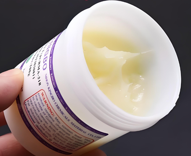
Solder paste contributes to component misalignment when the deposit is off center, uneven, or unable to hold the part securely before reflow. It can affect where the component sits after placement and how the molten solder pulls it during reflow.
- Stencil misregistration: Paste lands away from the pad center, creating an off-center seating surface and wetting target.
- Uneven paste volume: One termination receives more solder than the other, so support and reflow forces are no longer balanced.
- Blocked or damaged apertures: Deposit shape or volume changes from pad to pad and may repeatedly affect the same location.
- Inconsistent paste height: The component can tilt or contact one deposit before the other, increasing the chance of movement.
- Poor PCB support: Board movement during printing changes stencil gasketing, deposit position, or thickness in a local area.
- Low paste tack: A correctly placed component has less resistance to conveyor acceleration, vibration, or handling.
How to confirm: Compare SPI position, height, area, and volume on both sides of the affected component. Correct the print process if the deposit is already offset or asymmetric; do not move the placement coordinates to compensate for a paste-printing error.
Which Pick-and-Place Problems Cause Component Misalignment?
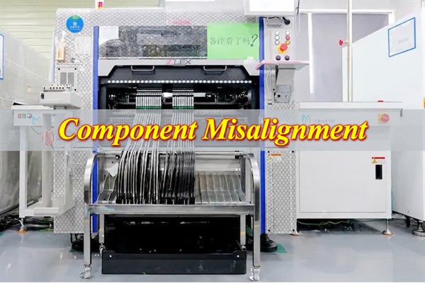
Pick-and-place faults create misalignment when the component is presented, centered, carried, or released differently from the position assumed by the program. The error often follows a particular feeder, nozzle, head, package, or board location.
- Feeder presentation: Poor tape indexing, a damaged pocket, or inconsistent component seating causes the same part type to be picked off center repeatedly.
- Nozzle condition: A worn, dirty, damaged, or unsuitable nozzle lets the component sit off center or rotate during travel.
- Vacuum stability: Low or unstable vacuum allows the part to slip between pickup and placement, producing variable offsets.
- Pickup position: A programmed pickup offset or drifting feeder position leaves too much error for component centering to correct reliably.
- Vision settings: Incorrect body dimensions, lead data, lighting, threshold, or polarity features create a false component center.
- Machine calibration: Camera, head, nozzle, or axis drift produces a repeated directional error across the affected equipment path.
- Placement height or force: Excessive force can squeeze or rebound the component, while insufficient travel may leave it poorly seated in the paste.
- PCB support: Local flex or warpage changes the real surface height and can make placement position vary by board area.
How to confirm: Review the pickup image, component-centering result, rejection log, nozzle and feeder records, and the position immediately after release. Check whether the offset follows the same feeder, nozzle, head, package, or PCB location.
Why Do Correctly Placed Components Move Before Reflow?
A component can be centered at placement exit and still move before reflow if paste retention is weak or the board experiences acceleration, vibration, flex, handling, or physical contact.
- Low solder paste tack: The component is easier to disturb during the time between printing and reflow.
- Excessive placement force or rebound: The part or board springs back after release and changes position.
- Fast conveyor acceleration: A sudden speed change can slide a light or poorly retained component.
- Rail or machine vibration: Repeated movement can rotate or shift parts before the paste reaches reflow temperature.
- Manual handling: Carrying, rotating, or setting down the assembly can disturb components that have not yet been soldered.
- PCB flex or unstable support: Board movement changes the contact between the component and paste deposits.
- Fixture interference: Contact with rails, tooling, covers, or nearby equipment can push the component directly.
How to confirm: Compare the component immediately after placement and again near the reflow entrance. If the first image is centered and the second is not, inspect paste tack, conveyor motion, support, handling, and physical clearance along that path.
Why Do Components Shift or Rotate During Reflow?
Molten solder tends to self-align a component only when the wetting and surface-tension forces on its terminations are reasonably balanced. Unequal forces can instead pull or rotate the part away from center.
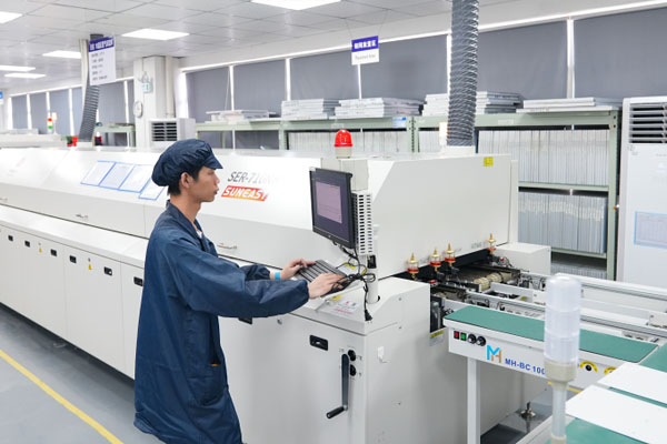
- Unequal paste volume: Different solder volumes create unequal wetting forces and stand-off at the two sides of the component.
- Asymmetric pad geometry: Different pad sizes or shapes provide unequal wetting areas and can pull the part in one direction.
- Uneven wetting: One termination wets sooner or more strongly than the other and moves the component before both joints stabilize.
- Oxidation or contamination: Delayed wetting on one pad or termination creates a temporary force imbalance.
- Thermal imbalance: Different copper areas or thermal masses cause the two joints to reach liquidus at different times.
- PCB or package warpage: Changing contact and stand-off alters when and where each joint wets.
- Airflow or vibration: A light component can move before the molten joints solidify, especially when paste retention and wetting are already uneven.
How to confirm: Compare SPI results and the verified oven-entry position with post-reflow AOI. If the part is centered at oven entry and offset after reflow, investigate paste balance, pad geometry, surface condition, thermal behavior, warpage, airflow, and vibration.
How Can SMT Component Misalignment Be Corrected?
Correct the first process condition that created the offset, then verify the result at that same inspection point. Avoid compensating for an upstream error with a downstream machine adjustment.
| Cause | What to Correct | How to Verify |
| Incorrect coordinate, rotation, origin, or panel data | Correct the approved centroid/CPL data and placement program | Recheck the data overlay and first-article position |
| Fiducial recognition or board transform error | Restore mark condition, lighting, selection, search settings, and panel mapping | Confirm that the common board-wide offset is removed |
| Offset or unbalanced paste deposits | Correct stencil alignment, aperture condition, printer setup, paste control, and PCB support | Confirm deposit position and side-to-side volume balance with SPI |
| Feeder, nozzle, vacuum, pickup, or vision fault | Service the affected hardware and correct pickup or package-library settings | Review pickup images, centering data, and as-placed position |
| Incorrect placement height, force, or board support | Correct package height, Z settings, placement force, support, and warpage control | Check seating and rebound immediately after release |
| Movement during board transfer | Stabilize conveyor motion, handling, support, clearances, and paste retention | Compare placement-exit and reflow-entry positions |
| Unbalanced reflow forces | Correct paste balance, pad asymmetry, contamination, thermal imbalance, warpage, airflow, or vibration | Compare pre-reflow and post-reflow positions |
After the first-stage check passes, inspect the completed solder joints and electrical clearances. This confirms that the correction fixed both the placement error and its effect on the finished assembly.
How Can You Prevent Component Misalignment from Recurring?
Prevention depends on preserving stage-by-stage evidence and watching for drift before the offset becomes a repeated defect.
- Keep first-article placement records so program, registration, and package-center changes can be compared with an approved baseline.
- Monitor SPI position and volume trends instead of relying only on a final pass/fail result.
- Track feeder, nozzle, vacuum, and calibration drift and service the affected item when its results begin to change.
- Review recurring AOI offset patterns by component type, reference designator, feeder, head, panel position, and board location.
- Control handling and transfer conditions when parts are correctly placed but move before reflow.
- Verify every process change at the stage where the offset first appeared before using final inspection to close the corrective action.
A useful record does more than show that the last board passed. It shows whether paste deposits, placement position, transfer stability, and post-reflow results remain centered over time.
FAQs About SMT Component Misalignment
Q1: How much SMT component misalignment is acceptable?
A1: There is no universal percentage that applies to every package and product. Acceptance depends on terminal-to-pad overlap, solder-joint condition, electrical clearance, package geometry, product class, and the applicable customer or workmanship requirement.
Q2: Can a misaligned component still pass AOI?
A2: Yes. AOI uses programmed limits and image features, so a component may pass if the offset remains inside those limits even though an engineer wants a closer review. Confirm the AOI program, actual solder-joint condition, and required acceptance criteria rather than treating the pass result as the only decision.
Q3: Can solder reflow correct a slightly misaligned component?
A3: Balanced molten-solder forces can pull a slightly displaced component toward center. However, self-alignment is not guaranteed when paste volume, pad geometry, wetting, temperature, or component contact is uneven.
Q4: Why does the same component keep shifting in the same direction?
A4: A repeated direction usually points to a stable input or equipment condition, such as an incorrect coordinate, package center, feeder position, nozzle offset, fiducial transform, or paste-print offset. Check which item the error follows across several boards.
Q5: Why do only a few components on the PCB become misaligned?
A5: Local defects often follow a package, feeder, nozzle, pad design, paste deposit, board-support point, or thermal area. Compare the affected parts with nearby known-good components at the same process stage to isolate what is different.
Q6: Why are 0201 and 0402 components more sensitive to placement errors?
A6: Their low mass and small contact area make pickup error, paste imbalance, airflow, vibration, and pad asymmetry large relative to the component size. Stable printing, suitable tooling, gentle transfer, and inspection resolution become more important as the package shrinks.
Q7: Can PCB warpage cause component misalignment?
A7: Yes. Warpage can change stencil contact, board height under the placement head, component seating, and joint contact during reflow. Check whether the offset follows a board area, panel location, support condition, or thermal cycle.
Q8: Can component misalignment cause open or short circuits?
A8: Yes. Too little terminal overlap can contribute to an open or weak joint, while displacement toward a neighboring pad can reduce clearance or contribute to bridging. The actual risk depends on package pitch, pad geometry, solder condition, and the amount and direction of the offset.
Q9: Should a misaligned SMT component always be reworked?
A9: No. Rework is required when the assembly fails the applicable acceptance criteria or presents a credible electrical, mechanical, or reliability risk. Use the contracted customer and workmanship requirements instead of reworking every visible offset or accepting every part that still functions.
Q10: What inspection data should be saved when misalignment keeps recurring?
A10: Save the approved placement data, fiducial results, SPI measurements, pickup and centering images, feeder and nozzle records, as-placed position, pre-reflow position, and post-reflow AOI or X-ray result. These records reveal the first point where the component moved and whether the corrective action remained stable.
Conclusion
Component misalignment is easiest to solve when you compare the component’s position from one SMT stage to the next. Start with the intended target, then check SPI, the as-placed position, the transfer path, and the post-reflow result. The first stage that shows the offset is where the corrective action should begin.
If you are reviewing a recurring SMT placement defect, send the affected reference designators, assembly drawing, centroid/CPL file, Gerber data, package details, SPI and AOI images, and relevant placement or reflow records to sales@bestpcbs.com. Request a stage-by-stage manufacturability review and a corrective-action plan tied to the evidence available for your build.