Printed circuit board etching selectively removes exposed copper to form the required conductor pattern. The finished geometry depends on resist definition, copper thickness, lateral undercut, etchant condition, spray distribution and exposure time. A stable process must control both copper removal and the trace width, spacing and edge profile that remain.
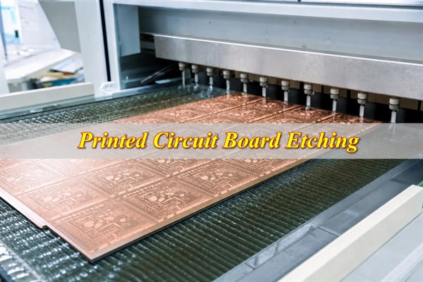
What Is Printed Circuit Board Etching and What Does It Control?
Printed circuit board etching removes unprotected copper and directly controls finished trace width, spacing, edge profile and pattern continuity. Imaging determines where copper should remain, while the etching step converts that protected image into physical conductors. Stripping and inspection then reveal whether the finished layer matches the released geometry.
Three geometries must be kept separate. The design geometry is the released CAD requirement. The production image may include validated CAM compensation. The finished geometry is the copper measured after etching. Treating these as identical hides the effect of side attack, plating buildup and process variation.
- Trace width: determines conductor cross-section, resistance, current margin and a key input to the impedance model.
- Spacing: affects isolation, voltage clearance and the risk of residual-copper shorts.
- Edge profile: reveals undercut, notches and roughness that may reduce the usable conductor area.
- Pattern integrity: includes opens, shorts, pinholes, residual copper and missing or malformed features.
- Panel consistency: shows whether the same feature remains stable across locations, orientations and production lots.
How Does the Printed Circuit Board Etching Process Work Step by Step?
The printed circuit board etching process follows a controlled image–remove–verify sequence. The exact resist and stripping operations differ between inner and outer layers, but each route must deliver clean exposed copper, intact protected features, complete unwanted-copper removal and measurable finished geometry.
- Prepare and inspect the copper surface. Remove oil, oxidation, fingerprints and particles, then confirm that the surface condition is uniform. Contamination or excessive roughness can weaken resist adhesion and later appear as pinholes, notches or missing copper.
- Apply the imaging resist. Laminate or coat the copper with the specified photoresist under controlled temperature, pressure and cleanliness. The resist must cover the panel without wrinkles, trapped particles, edge lifting or thickness variation.
- Expose the circuit image. Align the production artwork or direct-imaging data to the correct layer, then expose the resist so required conductors remain protected. Registration, exposure energy and data revision must be verified before development.
- Develop and inspect the pattern. Develop away the soluble resist so that only the copper scheduled for etching is exposed. Check fine spaces, pad edges and registration for resist scum, damaged edges, incomplete development or unintended openings.
- Prepare the outer-layer etch resist where required. In a common pattern-plating route, plate copper onto the hole walls and exposed circuit features, add a compatible metallic etch resist, and strip the remaining photoresist. Inner layers normally proceed with photoresist protecting the required circuit copper directly.
- Etch the exposed copper. Match the chemistry to the resist system and control copper loading, temperature, spray pressure, nozzle condition, drainage and conveyor speed. Remove the field copper completely while limiting lateral attack beneath protected trace edges.
- Strip the temporary protection. Remove the photoresist or metallic etch resist using the specified process without attacking the finished conductor. Residue must not hide shorts, interfere with inspection or contaminate later lamination and finishing steps.
- Inspect and release the layer. Use AOI to locate pattern defects, dimensional measurement to verify critical widths and spaces, and microsection or electrical evidence where the order requires it. Release the layer only after its results are linked to the correct revision and production lot.
A defect found after printed circuit board etching is not automatically an etcher problem. A repeated missing feature may originate in the source image, while random notches may point to resist damage. Location-dependent width change is more consistent with spray, drainage or panel-loading variation. Root-cause analysis must follow the defect pattern back through the complete route.
Why Are Inner-Layer and Outer-Layer PCB Etching Processes Different?
Inner and outer layers use different printed circuit board etching routes because their copper construction and protection requirements are different. An inner layer normally begins as copper foil on a laminate core and uses photoresist to protect the required image. An outer layer must also preserve plated hole walls and the copper added to the surface during pattern plating.
| Process Element | Inner Layer | Outer Layer |
| Starting copper | Copper foil bonded to a laminate core | Drilled panel with plated holes and surface copper |
| Circuit protection | Imaged photoresist protects required copper | Pattern-plated metal protects traces, pads and plated-hole features |
| Etch target | Remove exposed foil while retaining the imaged circuit | Remove exposed surface copper while retaining plated traces, pads and hole features |
| Common chemistry | An acidic route is commonly compatible with the photoresist process | An alkaline route is commonly compatible with the metallic etch resist |
| Main process risk | Registration or width defects become inaccessible after lamination | Excessive lateral attack reduces conductors while plated features must remain protected |
| Release evidence | Registration, AOI and critical dimensions before lamination | AOI, critical dimensions, spacing and plated-feature integrity |
“Acid for inner layers and alkaline for outer layers” is a useful process map, not a universal recipe. The selected chemistry must be compatible with the actual resist, plating sequence, equipment and regeneration controls. A detailed copper PCB etching solution review belongs at the chemistry-selection level; this article uses chemistry only to explain the manufacturing route.
How Do Etch Factor and Undercut Affect PCB Trace Width?
In printed circuit board etching, undercut narrows the top of a trace, while the etch factor indicates how much lateral width is lost relative to the copper removed vertically. More undercut leaves a smaller conductor cross-section and a more pronounced trapezoidal profile. For the same copper thickness, a higher etch factor generally means less lateral attack, although finished width and spacing remain the acceptance requirements.
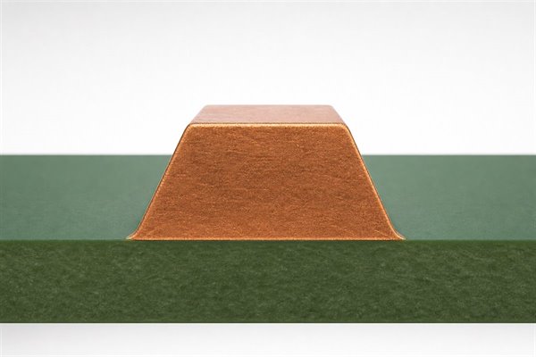
Using a one-side convention, etch factor = copper thickness ÷ undercut on one side. If 35 µm of copper is removed vertically and the measured one-side undercut is 10 µm, the etch factor is 35 ÷ 10 = 3.5:1. With similar loss on both sides, the protected top feature can lose approximately 20 µm in total width.
A cross-section provides the same information from measured geometry. If the conductor base is 120 µm wide and the top is 100 µm wide, the one-sided difference is (120 − 100) ÷ 2 = 10 µm. The report should identify the measured width, cross-section location and whether undercut is stated per side or as total width loss.
A higher etch factor generally indicates less lateral loss for the same vertical depth, but it is not a universal acceptance criterion. Finished trace width, remaining cross-sectional area, spacing and the drawing tolerance remain the actual product requirements.
How Do Copper Thickness and Etching Affect Finished Trace Width?
In printed circuit board etching, thicker copper increases the vertical removal distance and usually reduces the process margin available for fine traces and spaces. Removing 70 µm of exposed copper requires a deeper etch path than removing 35 µm. The additional exposure creates more opportunity for lateral attack, but the width loss does not scale by one fixed multiplier across every chemistry, layout and machine.
The relevant input is the PCB copper thickness present at the etching stage. On an inner layer, this is closely related to the selected foil. On an outer layer, pattern plating can increase the copper thickness that the etch must clear between protected features. A drawing that states only “1 oz copper” without distinguishing starting and finished copper may therefore be incomplete.
Local pattern density also changes the etching response. An isolated narrow trace beside a large open area may not etch like the same trace inside a dense field. Panel orientation, copper distribution and drainage can all create position-dependent results. Minimum line-and-space capability should be evaluated with copper thickness, layer type and surrounding pattern density.
How Is Artwork Compensation Used to Control Etched Trace Width?
Artwork compensation for printed circuit board etching adjusts the production image so the measured feature approaches the released finished dimension. It is a fabricator-controlled CAM operation derived from a validated process window. It is not a universal amount that should be added to every CAD trace before quotation.
An initial estimate may use the expected two-sided width loss, but production compensation also reflects imaging, resist behavior, layer route, copper thickness, equipment, pattern density and measured process history. Enlarging one feature reduces the adjacent clearance, so CAM must protect trace width and spacing together.
- Lock the requirement: identify the released finished width, spacing and tolerance instead of treating CAD artwork as the only acceptance reference.
- Classify the layer: separate inner-layer foil from plated outer-layer copper because the etch depth and resist route differ.
- Model vulnerable features: review isolated fine lines, neck-downs, fine-pitch pads and impedance structures rather than applying one global enlargement blindly.
- Check the trade-off: confirm that widening a conductor does not consume a mandatory clearance or alter pad-to-feature relationships.
- Control the output: keep compensated production data linked to the correct released revision and documented DFM approval.
Which Printed Circuit Board Etching Materials and Process Variables Control Uniformity?
Printed circuit board etching uniformity is controlled by the copper surface, resist definition, etchant condition, temperature, spray delivery, exposure time and panel layout. These variables work as one process window: stable bath readings cannot compensate for poor cleaning, damaged resist, blocked nozzles, uneven drainage or an imbalanced copper pattern.
- Copper surface: oxidation, oil, particles and inconsistent conditioning can weaken resist adhesion or change local reaction behavior.
- Resist definition: exposure, development, edge quality, adhesion and pinholes determine which copper remains protected.
- Etchant condition: concentration and dissolved-copper loading affect removal rate; pH, specific gravity or ORP are useful only where they belong to the validated control plan.
- Temperature: changes reaction rate and must be controlled with the chemistry and equipment rather than copied as an isolated universal setting.
- Spray delivery: nozzle condition, pressure, angle, shadowing and drainage influence how fresh chemistry reaches the surface.
- Exposure time: conveyor speed must remove all unwanted copper without leaving the protected feature in the etchant longer than necessary.
- Panel layout: copper density, orientation, leading-edge effects and solution retention can create within-panel variation.
No single setpoint proves that the process is uniform; the stronger signal is how process readings track with measured geometry. If trace width drifts while bath readings remain stable, inspect imaging, nozzles, transport and panel distribution. A similar shift across all panel positions points more strongly to chemistry or exposure time. Trend product measurements alongside process inputs.
What Causes Common PCB Etching Defects?
Common printed circuit board etching defects are caused by incomplete development, damaged resist, incorrect exposure time, uneven spray delivery, unstable etchant conditions or unsuitable CAM compensation. The visible defect alone does not identify the source: the same open circuit may result from missing artwork, a resist pinhole or excessive local copper loss. Diagnosis must therefore use the defect type, location and repetition pattern.
| Defect | Likely Causes | Verification | Correction Direction |
| Residual copper | Resist scum, short dwell, weak spray or high local copper loading | AOI, magnified inspection and panel-location map | Separate blocked copper exposure from insufficient etching before changing the process |
| Copper bridges or shorts | Incomplete development, trapped solution, local shadowing or insufficient field-copper removal | AOI, continuity/isolation test and microscopy | Correct development or spray access, then verify the affected spacing across the panel |
| Narrow conductors | Excess dwell, lateral attack, weak resist edges or insufficient CAM compensation | Width measurements across locations and orientations | Separate process drift from artwork error and compare results with the finished-width requirement |
| Notches or breaks | Resist pinholes, scratches, contamination or local spray concentration | AOI, microscopy and pre-etch resist inspection | Correct cleaning, handling or resist integrity before adjusting the etchant |
| Rough edges | Poor resist definition, unstable reaction or uneven surface condition | Edge microscopy and cross-section where critical | Check imaging and surface preparation, then confirm chemistry and spray stability |
| Panel-position variation | Nozzle pattern, drainage, transport, orientation or copper imbalance | Repeated measurements mapped by panel coordinate | Correct equipment or panel strategy according to the repeatable location pattern |
Map whether a defect follows a circuit feature, panel coordinate, trace orientation or entire lot. Repetition on the same feature points toward data or imaging; repetition at the same panel position suggests equipment or transport. A lot-wide shift is more consistent with shared material or process conditions. This pattern-based approach directs corrective action toward the source rather than the symptom.
How Are Etched PCB Features Inspected and Verified?
Printed circuit board etching is verified by combining pattern inspection, dimensional evidence and electrical testing. No single method proves all three. An AOI pass does not establish every critical width, and an electrical pass does not prove that a conductor has the required cross-section.
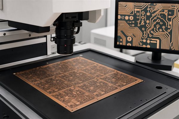
- Confirm the inspection reference. Match the layer to the approved artwork, fabrication drawing, netlist and revision. Define the product class, critical features, sampling plan and measurement method before results are accepted.
- Run automated optical inspection. Compare the etched image with controlled data to identify opens, shorts, residual copper, notches and missing or extra features. Review repeated detections by feature and panel position rather than relying on the total machine count.
- Measure critical geometry. Check specified trace widths, spaces, annular features and registration using calibrated equipment and a documented sampling plan. Record the measurement location and whether a reported width is the top, base or optical surface width.
- Examine the conductor cross-section where necessary. Use a microsection or representative coupon to verify copper thickness, top and base widths, sidewall profile and undercut. This evidence is especially useful for fine traces, thick copper and controlled-impedance structures.
- Verify electrical connectivity. Test continuity and isolation against the released netlist after the conductor pattern is complete. Electrical testing can confirm opens and shorts, but it cannot prove that every conductor meets its dimensional or cross-sectional requirement.
- Review and retain the release evidence. Process nonconforming results under the agreed acceptance procedure, then link AOI, dimensional, cross-section and electrical records to the correct revision, panel or lot. Release the layer only when the specified requirements are supported by the required evidence.
For printed circuit board etching, IPC-A-600 can support visual acceptability assessment, while IPC-6012 can define performance and qualification requirements for rigid printed boards when invoked by the contract. Neither document removes the need to state the product class, drawing requirements and agreed measurement method. Acceptance must be tied to the applicable order requirements, not to a standard name used without scope.
How Does PCB Etching Affect Fine Traces and Controlled Impedance?
Printed circuit board etching affects controlled impedance by changing the conductor width and sidewall profile of the transmission line. Dielectric thickness, dielectric properties, copper thickness and reference-plane geometry also matter, but a conductor narrower than the modeled value can shift impedance away from its target even when the laminate and stackup are correct.
A trapezoidal trace does not have one universally representative width. A field solver may use the top width, base width or the full sidewall profile. The drawing and impedance model should identify the stackup, target, tolerance, reference layers and finished copper condition so that the modeled geometry reflects the selected production process.
Fine traces have less absolute width margin. Thick copper, isolated neck-downs and dense routing can further restrict the usable process window. Impedance release should connect modeled geometry, finished measurements and coupon results rather than relying on the nominal CAD width alone.
What PCB Design Inputs Reduce Etching Risk Before Fabrication?
The design inputs that reduce etching risk are clear copper requirements, manufacturable trace and spacing, identified critical features, balanced copper distribution and one consistent data revision. CAM compensation can correct a validated process allowance, but it cannot resolve contradictory files or geometry whose required width and clearance cannot both be preserved.
- Define copper correctly: distinguish starting foil, plated copper and required finished copper for each relevant layer.
- Use realistic geometry: reserve minimum trace and spacing for unavoidable locations instead of applying the limit across the complete board.
- Identify critical dimensions: flag impedance nets, fine-pitch pads, neck-downs, safety clearances and current-carrying conductors.
- Review copper distribution: check isolated fine lines beside large clear areas, dense fields and strongly unbalanced panel regions.
- Align every file: resolve conflicts among Gerber or ODB++, drill data, netlist, stackup, fabrication drawing and revision notes.
- Approve DFM exceptions: document any geometry change, compensation exception or acceptance decision before tooling.
A useful DFM response should identify the exact layer and feature, the released requirement, the predicted manufacturing risk and the proposed disposition. “Use best effort” is not an acceptance criterion. Resolve critical etching exceptions before the production image is released.
What Information Should Be Confirmed Before PCB Fabrication?
Before fabrication, confirm the image data, drill files, fabrication drawing, stackup, copper construction, critical geometry, impedance requirements, acceptance evidence, quantity and revision. Every file must describe the same board, and every dimension requiring special control must be identifiable before CAM and tooling begin.
- Image data: submit Gerber or ODB++, aperture information where required, drill files and a netlist generated from the same released revision.
- Fabrication drawing: define board dimensions, layer order, material notes, surface finish and any controlled features.
- Copper construction: state the starting foil and required finished copper where applicable, avoiding ambiguous shorthand.
- Critical geometry: identify the minimum trace and spacing, local tolerances, fine-pitch areas and any dimension that cannot be altered during CAM.
- Impedance control: provide target values, tolerances, reference layers, stackup constraints and coupon requirements.
- Acceptance evidence: specify the applicable class, electrical test, dimensional records, coupon or microsection needs and document retention.
- Order context: provide prototype and production quantities, expected follow-on volume and the controlled revision status.
Before approving printed circuit board etching for production, confirm four gates: the files agree, the copper construction is clear, the critical dimensions are manufacturable, and the inspection plan can prove the requirement. Quotation differences are difficult to compare when suppliers are evaluating different assumptions.
FAQs About Printed Circuit Board Etching
Q1: How long does industrial PCB etching take?
A1: The machine exposure depends on the copper depth to be removed, etchant condition, temperature, spray transfer and conveyor setting. It cannot be converted into one universal time. Cleaning, imaging, development, stripping and inspection also occur around the etch step, so etcher dwell time is not the same as PCB manufacturing lead time.
Q2: Can solder mask compensate for an over-etched trace?
A2: No. Solder mask protects selected surfaces and defines solderable openings, but it does not restore copper removed from a conductor. A trace below its dimensional requirement must be dispositioned against the applicable acceptance criteria. Covering the trace cannot recover its cross-sectional area, resistance margin or impedance geometry.
Q3: Can PCB etching defects be repaired after manufacturing?
A3: Some localized conductor defects may be repairable under an approved procedure, but the decision depends on defect type, location, product class and contractual acceptance. Widespread width loss, repeated process defects or residual-copper spacing violations may require rejection. Any permitted repair needs documented authorization, inspection and traceability.
Q4: Does PCB surface finishing happen before or after etching?
A4: The permanent solderable surface finish is generally applied after the outer-layer conductor pattern has been formed and solder mask has defined the exposed pads. Temporary metal used to protect a pattern during outer-layer etching serves a different manufacturing role. An etch resist must not be confused with the final surface finish specified on the fabrication drawing.
Q5: Can the etching process damage plated through-holes?
A5: Outer-layer processing is designed so the metallic resist protects the required pattern, including the copper associated with plated features, while exposed surface copper is removed. Incomplete protection or an unsuitable process can still create damage. Hole reliability must be evaluated through the complete drilling, desmear, plating, etching and inspection sequence, not etching alone.
Q6: Does etching change pad dimensions as well as trace width?
A6: Yes. Lateral copper loss can affect pads, neck-downs and other protected features as well as straight traces. Compensation must therefore evaluate the complete image. Pad diameter, annular-ring intent, neighboring clearance and later solder-mask registration must remain compatible; enlarging every feature globally can solve one width problem while creating a spacing problem.
Q7: Is ferric chloride suitable for industrial PCB production?
A7: Ferric chloride removes copper and is common in laboratory or small-scale work, but that does not make it the automatic choice for a controlled production line. Industrial selection considers resist compatibility, regeneration, copper loading, equipment, process monitoring and waste controls. Repeatability and compatibility with the complete route matter more than chemical familiarity alone.
Q8: What is the difference between PCB etching and PCB milling?
A8: Etching removes exposed copper around a protected image, while milling uses a cutting tool to create isolation paths. Milling can be useful for selected prototypes but introduces tool-diameter, wear, burr and flatness limits. It also does not replace multilayer registration or plated-hole processing. The two methods are not direct production equivalents.
Q9: Why is a pilot lot useful before volume production?
A9: A pilot lot checks whether the released data, copper construction, compensation and inspection plan work together on the intended route. It is particularly useful for fine lines, thick copper, tight impedance tolerance or a new stackup. Pilot evidence should close documented DFM questions before volume release, but it does not replace production control or lot acceptance.
Q10: Which records should be requested for critical etched features?
A10: The required record set depends on product risk and the purchase specification. It may include approved DFM exceptions, controlled fabrication data, AOI status, dimensional measurements, electrical-test status and relevant coupon or microsection results. The essential requirement is traceability to the correct revision, panel or lot and acceptance decision, with an agreed retention period.
Reliable printed circuit board etching depends on dimensional control throughout the production route. The production image, copper construction, etch behavior and inspection plan must work as one system.
For a fabrication review and quotation, email sales@bestpcbs.com. Submit your Gerber or ODB++ data, drill files, fabrication drawing, stackup, finished-copper requirements, minimum trace and spacing, impedance targets, quantity and inspection requirements. The review can then identify etching-sensitive geometry, conflicting specifications and verification needs before tooling and production release.