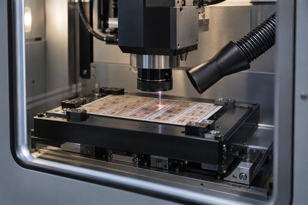
Printed circuit board dicing is a precision cutting process that separates individual PCBs or circuit substrates from a larger panel using an abrasive blade or a laser. It is commonly considered for ceramic substrates, miniature circuits, and applications requiring narrow cutting streets or tightly controlled edges.
The challenge is not simply separating the boards. An unsuitable cutting method can cause chipped edges, microcracks, burrs, or damaged conductors, even when the finished dimensions appear correct. This article explains how PCB dicing works, which materials and applications benefit from it, and how to control cutting quality.
What Is Printed Circuit Board Dicing?
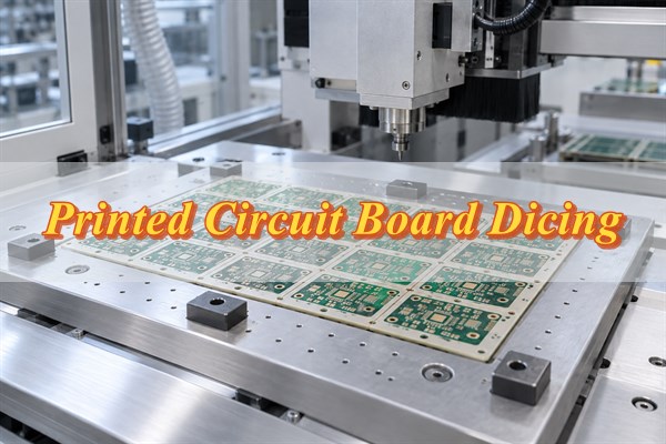
Printed circuit board dicing is a precision singulation process that removes material along defined cutting paths to separate individual circuits. It is particularly useful when brittle substrates, narrow cutting streets, or strict edge requirements make conventional breakaway separation unsuitable.
PCB dicing is related to two other manufacturing terms, but they are not identical:
- PCB dicing: Precision cutting, traditionally using a thin abrasive blade, although laser-based precision separation is also described as laser dicing.
- PCB singulation: The general separation of individual circuit units from a larger panel or substrate.
- PCB depaneling: Removing PCBs from a production panel using methods such as routing, V-scoring, or laser cutting.
For example, a standard FR-4 PCB may be separated using routed tabs or V-scoring. A brittle ceramic substrate containing closely spaced circuits may instead require precision blade dicing or a qualified laser process.
How Does the Printed Circuit Board Dicing Process Work?
The PCB dicing process involves six stages: reviewing the cutting requirements, securing the substrate, setting the cutting parameters, aligning the equipment, performing the cut, and inspecting the separated boards.
Step 1: Review the PCB Layout and Cutting Requirements
Confirm the finished dimensions, material, thickness, cutting street width, and copper clearance. Identify components or other protected features near the proposed cutting path.
Step 2: Secure the PCB or Substrate
Position the workpiece using a suitable fixture, carrier, or adhesive support tape. Proper support prevents movement and helps protect thin or brittle substrates during separation.
Step 3: Set the Cutting Parameters
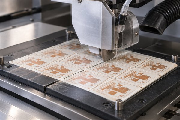
For blade dicing, select the blade specification, spindle conditions, feed rate, and cutting depth. For laser dicing, establish the laser settings, focus position, scanning speed, and number of passes.
Step 4: Align the Cutting Tool
Align the blade or laser with the defined cutting streets using suitable reference features. Verify the position before cutting, particularly when conductive features are close to the finished edge.
Step 5: Perform the Dicing Operation
Follow the approved cutting path and sequence while maintaining workpiece stability. The cutting sequence should prevent separated units from shifting or contacting the tool.
Step 6: Clean and Inspect the Separated Boards
Remove cutting debris or process residues as required. Check finished dimensions, edge condition, and cleanliness against the agreed specifications.
The result should be more than a fully separated board. Each unit must retain its required dimensions, structural integrity, and electrical condition after cutting.
What Are the Main Methods of PCB Dicing?
Blade dicing and laser dicing are two main precision cutting methods used for PCB and circuit substrate separation. They differ in how material is removed, the cutting geometry they support, and the defects that must be controlled.
| Factor | Blade Dicing | Laser Dicing |
|---|---|---|
| Cutting Principle | Mechanical abrasion | Laser material removal |
| Cutting Tool | Thin rotating abrasive blade | Focused laser beam |
| Cutting Geometry | Primarily straight cuts | Straight and complex contours |
| Mechanical Stress | Requires control of cutting forces | Minimal direct mechanical cutting force |
| Suitable Materials | Commonly rigid, brittle substrates | Depends on laser type and material stack |
| Main Edge Risks | Chipping, cracks, burrs | Thermal damage, residue, taper |
| Main Process Controls | Blade condition, feed, depth, coolant | Pulse settings, focus, scanning, passes |
Which PCB Materials Are Suitable for Dicing?
Ceramic circuit substrates, thin rigid PCBs, and certain electronic package substrates are common candidates for precision dicing. Flexible and mixed-material circuits may also require precision cutting, although a laser process is often more appropriate for these constructions.
The main material considerations are:
- Ceramic PCBs: Alumina (Al₂O₃) and aluminum nitride (AlN) are hard, brittle materials. Blade dicing and suitable laser processes may be used, with particular attention to chipping, microcracks, and dimensional accuracy.
- Thin Rigid PCBs: Thin FR-4 and similar laminates may require stable support during cutting. Their glass fibers, resin, and copper layers respond differently to mechanical cutting and laser energy.
- Flexible and Rigid-Flex PCBs: Polyimide-based circuits can deform under mechanical loading. Laser cutting can produce fine contours without direct cutting force, but adhesive layers, copper, and local heat effects still require evaluation.
- Metal-Backed PCBs: Aluminum-backed and copper-backed boards are more challenging because the conductive backing and dielectric layers have different cutting characteristics. Metal burrs, tool wear, and heat input require additional attention.
Material thickness, copper distribution, surface films, and layer construction also affect cutting performance. A process qualified for one substrate should not be reused on another material without review.
Where Is Printed Circuit Board Dicing Used?
Printed circuit board dicing is used where circuit dimensions, material properties, or edge requirements call for precision separation. Typical applications involve brittle substrates, miniature circuits, specialized electronic modules, and delicate circuit constructions.
1. Ceramic Circuit Substrates
Ceramic substrates are used in power electronics, high-temperature circuits, and applications requiring electrical insulation and thermal performance.
Multiple circuits may be produced on a larger ceramic sheet. Precision dicing separates them while controlling edge chipping, cracking, and dimensional variation.
2. RF and Microwave Circuits
Some RF and microwave circuits use specialized high-frequency laminates or ceramic substrates. The finished outline may need to meet tight mechanical requirements, especially near board-edge interfaces.
Precision cutting can be considered when conventional separation cannot meet the specified dimensions or edge condition. Copper clearance and material compatibility must be evaluated before processing.
3. Miniature Electronic Modules
Miniature electronic modules may contain many small circuit units arranged closely together. Limited separation space can make conventional breakaway tabs or mechanical routing impractical.
A suitable precision dicing process can control cutting location while reducing the risk of damaging adjacent circuit features.
4. Electronic Package Substrates
Certain electronic package substrates and substrate-like circuit assemblies require accurately positioned separation cuts.
Narrow cutting streets and nearby conductors can make kerf control and edge integrity particularly significant. These substrates must be evaluated according to their actual construction rather than treated as conventional FR-4 panels.
5. Thin and Delicate Circuit Panels
Thin rigid PCBs, flexible circuits, and rigid-flex constructions may be sensitive to mechanical separation forces.
A qualified laser cutting process can reduce direct mechanical loading and accommodate complex contours, although thermal response and cleanliness requirements still need review.
Not every board used in these applications requires dicing. The method is selected when its cutting characteristics provide a practical advantage over conventional separation.
When Should You Use PCB Dicing Instead of Conventional Depaneling?
PCB dicing is worth considering when conventional V-scoring or routing cannot meet the material, cutting-clearance, or edge-quality requirements.
Typical situations include:
- Brittle Materials: Ceramic substrates may crack when subjected to uncontrolled breakaway forces.
- Narrow Cutting Streets: Closely spaced circuits may require a smaller, more accurately controlled cutting path.
- Miniature Board Dimensions: Small circuit units may require precise positioning and continuous support during separation.
- Strict Edge Requirements: Limits on chipping, burrs, cracks, or contamination may justify a specialized cutting process.
- Delicate Structures: Thin boards and circuits with sensitive nearby features may benefit from reduced separation forces.
However, conventional depaneling remains suitable for many standard PCB panels. If routing or V-scoring meets the outline, edge-quality, and mechanical-stress requirements, specialized dicing may add unnecessary processing cost.
The choice should be based on the finished-board requirements and an acceptable production yield, not on the assumption that a more specialized cutting process is always better.
What PCB Design Details Matter Before Dicing?
Before PCB dicing, the manufacturing data must define the cutting path, permitted material removal, protected circuit features, and finished-board tolerances.
The following details require review:
- Cutting Street Width: Specify the available corridor between adjacent circuits. It must accommodate the intended cut and positioning variation.
- Kerf Allowance: Define the permitted width and location of material removal.
- Copper Clearance: Identify conductors, plated features, and exposed copper near the cutting path.
- Board Thickness and Stackup: Provide the substrate material, dielectric construction, copper thickness, and backing layers.
- Component Clearance: For populated boards, confirm that components, solder joints, and connectors do not interfere with cutting or handling.
- Edge Tolerance: Specify allowable dimensional variation, chipping, cracks, burrs, and other relevant defects.
Cutting street and kerf are not interchangeable. The cutting street is the designated separation corridor, while the kerf is the actual width of material removed.
The expected kerf, including cutting and alignment variation, must remain within the permitted area. Neither the nominal blade thickness nor the laser spot diameter alone determines the final cut width.
Clearly defined requirements reduce the risk of cutting into functional features and make manufacturing feasibility easier to evaluate.
Which Parameters Affect PCB Dicing Accuracy and Edge Quality?
PCB dicing accuracy depends on tool condition, cutting parameters, material response, and workpiece stability. Incorrect settings can produce chipped edges, dimensional errors, excessive burrs, or incomplete separation.
For blade dicing, the main parameters include:
- Blade Specification: Abrasive grain size, concentration, bond type, and blade thickness influence material removal and edge quality.
- Spindle Speed: Must remain compatible with the blade specification and cutting conditions.
- Feed Rate: Excessive feed can increase cutting load and contribute to chipping or tool deflection.
- Cutting Depth: Must achieve the required separation without damaging the supporting carrier.
- Coolant Delivery: Where applicable, suitable coolant flow helps manage cutting heat, remove debris, and protect the blade.
For laser dicing, the main parameters include:
- Laser Wavelength: Determines how effectively different materials absorb laser energy.
- Pulse Duration: Influences energy deposition and the potential for thermal effects.
- Pulse Energy and Scanning Speed: Affect material removal, cutting efficiency, and heat accumulation.
- Focus Position: Influences kerf geometry, cutting depth, and sidewall condition.
- Number of Passes: Must provide complete separation without unacceptable damage to surrounding material.
In both methods, alignment accuracy, substrate flatness, and fixture stability affect the final cut.
Process parameters should be verified through representative cutting trials, especially when the material, thickness, or layer structure changes.
What Defects Can PCB Dicing Cause?
Common PCB dicing defects include edge chipping, microcracks, burrs, delamination, thermal damage, dimensional errors, and contamination. Their causes often involve a mismatch between the material, cutting method, support, and process settings.
- Edge Chipping: Small fragments break away from the cut edge, particularly on brittle substrates. Review the blade specification, cutting load, entry and exit conditions, and substrate support.
- Microcracks: Fine cracks may form during ceramic or brittle-material cutting. These can extend beyond visible chips and may require additional inspection.
- Burrs: Raised or smeared material can develop where the cutting path intersects copper or metal backing. Check tool condition and material removal settings.
- Delamination: Separation between layers can result from excessive mechanical loading or localized heating. The affected material interface should be examined.
- Thermal Damage: Unsuitable laser conditions may produce discoloration, carbonization, or other heat-affected material.
- Dimensional Errors: Tool misalignment, substrate movement, blade wear, or focus variation can shift the finished edge beyond tolerance.
- Contamination: Abrasive particles, cutting fluids, or laser-generated residues may remain on the PCB after separation.
Visible edge appearance alone does not establish structural quality. A board can meet its outline dimensions while containing hidden cracks or contamination near functional features.
Corrective action should be followed by repeat cutting and inspection to confirm that the defect has been reduced to an acceptable level.
How Can You Inspect the Quality of Diced PCBs?
Diced PCB inspection should verify the finished dimensions, edge integrity, cleanliness, and relevant electrical performance. The inspection plan must match the risks identified for the material and cutting method.
The main inspection methods include:
- Visual Inspection: Examine the cut perimeter for visible chips, cracks, burrs, exposed fibers, discoloration, and cutting residues.
- Dimensional Measurement: Verify the finished outline, critical edge locations, and specified tolerances using suitable measurement equipment.
- Magnified Inspection: Use optical magnification to assess small chips, cracks, and other defects that are difficult to evaluate visually.
- Structural Inspection: Where required, examine qualification samples using cross-sectioning or another agreed method to assess hidden cracking or delamination.
- Electrical and Functional Testing: For applicable boards, verify continuity, insulation, or relevant circuit functions after separation.
Inspection results should be compared against predefined acceptance criteria. For example, a ceramic substrate may have a specified maximum chipping allowance, while a metal-backed board may require additional inspection for conductive burrs.
Approved samples, process settings, and inspection records should be retained where required to maintain consistent acceptance decisions across production batches.
FAQs About Printed Circuit Board Dicing
Q1: Can a dicing blade cut through copper layers?
A1: Yes, with a suitable blade and qualified process. Copper may affect blade wear and produce burrs or smeared material, so clearance and edge quality must be checked.
Q2: Does a narrower kerf always improve cutting quality?
A2: No. A narrower kerf does not guarantee a better cut. Material behavior, cutting stability, and positioning accuracy also affect edge quality.
Q3: Can PCB dicing be performed after SMT assembly?
A3: Yes, in some applications. Component clearance, cutting forces, contamination, cleaning restrictions, and handling must be reviewed before processing populated boards.
Q4: Is laser scribing the same as full-cut laser dicing?
A4: No. Laser scribing creates a groove or weakened separation line, while full-cut laser dicing removes material through the required thickness to separate the units directly.
Q5: Can blade dicing produce curved PCB outlines?
A5: Conventional blade dicing is mainly suited to straight cuts. Laser cutting or routing is generally more practical for curved or complex PCB outlines.
Q6: Why is coolant used during blade dicing?
A6: Coolant helps control cutting heat and remove debris. It also helps protect the blade during operation. The coolant type and delivery must follow the equipment and blade manufacturer's requirements.
Q7: Can PCB dicing affect electrical insulation?
A7: Yes. Cracks, conductive burrs, or contamination can affect insulation. Copper clearance and appropriate post-cut inspection help reduce these risks.
Q8: Can one cutting recipe be used for different ceramic substrates?
A8: Not without evaluation. Alumina, AlN, and other ceramics differ in mechanical and thermal behavior, so their cutting conditions may need to be adjusted.
Q9: Is PCB dicing practical for low-volume prototypes?
A9: Yes, if a suitable cutting process is available. However, setup, fixtures, and qualification cuts may represent a significant portion of the total cost.
Q10: Does laser dicing always eliminate post-cut cleaning?
A10: No. Cleaning requirements depend on the laser process and material. Some processes produce very clean edges, while others may leave residues that require removal.
Conclusion
Printed circuit board dicing provides a controlled way to separate circuits when material properties, cutting dimensions, or edge-quality requirements make conventional PCB depaneling unsuitable. Blade dicing is commonly used for compatible rigid substrates and straight cuts, while laser cutting offers greater flexibility for delicate materials and complex contours. Reliable results depend on the material stack, cutting parameters, workpiece support, and inspection requirements.
For PCB projects involving ceramic substrates, thin rigid boards, or demanding cutting requirements, EBest Circuit provides PCB manufacturing, DFM review, and PCBA support. Send your Gerber files, material specifications, board thickness, quantity, and cutting requirements to sales@bestpcbs.com. Our technical team can review manufacturing feasibility and confirm the applicable production scope before quotation.