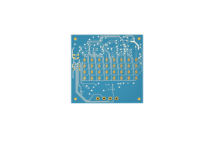
High-quality PCB prototype Germany plays a critical role in accelerating electronic project timelines, blending precision engineering with on-time delivery. Our PCB prototype Germany services meet the varied requirements of multiple industries, using cutting-edge technologies to produce reliable prototypes compliant with stringent European norms.
Why Choose PCB Prototype Germany?
Advantages of PCB Prototype Company:
- Precision Manufacturing: Adheres to rigorous German engineering standards, ensuring trace widths down to 50 µm and consistent board thicknesses from 0.4 mm to 7.0 mm.
- Localized Support: Proximity enables faster communication, reduced shipping delays, and compliance with regional regulations like RoHS and WEEE.
- Quality Material Sourcing: Uses premium materials from trusted brands like Panasonic and Nanya, including halogen-free high-Tg substrates for durability.
- Year-Round Reliability: Delivers consistent production even during international holidays, avoiding disruptions to project timelines.
- Technical Versatility: Supports complex processes such as HDI microvia, impedance control, and semi-flex deep milling for diverse applications.
Top 10 Best PCB Prototype Germany Manufacturer
| Company Name | Main Business | Core Advantages | Process Capabilities | Prototyping Lead Time |
| CONTAG AG | PCB prototyping and express manufacturing | Berlin production site; high-technology prototype focus | Rigid, multilayer, flex and rigid-flex PCB options | Prototype schedule: Confirm for construction and quantity |
| Schweizer Electronic AG | Embedded packaging PCB, high-reliability circuit boards | Founded 1849, European top 3 PCB maker | 2-16 layers, embedded components | 3-5 days (standard) |
| Weidmüller Group | Industrial-grade PCB, PCB connectors | UL/CSA certified, 80+ countries network | 2-8 layers, industrial-grade finishes | 4-6 days (standard) |
| Beta Layout GmbH | Rapid PCB prototyping, RFID-integrated PCB | UL certified Magic-PCB technology | 2-10 layers, RFID-embedded PCB | 2-3 days (standard) |
| Zollner Elektronik AG | High-reliability PCB, PCBA services | Automotive/aviation certification | 2-24 layers, HDI blind/buried vias | 5-7 days (standard) |
| Phoenix Contact GmbH | Industrial PCB, automation-related boards | ISO 9001 certified, 100+ years experience | 2-6 layers, anti-vibration design | 6-8 days (standard) |
| Würth Elektronik | RF/microwave PCB, passive components | IATF 16949 automotive certification | 2-12 layers, RF impedance control | 4-5 days (standard) |
| AT&S Austria (German Branch) | High-density HDI PCB, automotive boards | HDI technology leader | 4-20 layers, HDI blind/buried vias | 5-7 days (standard) |
| Eurocircuits GmbH | Prototype & small-batch PCB | Pan-European production network | 2-16 layers, rigid-flex PCBs | 3-4 days (standard) |
| HARTING Electronics | Heavy-duty industrial PCB | IP67 protection grade support | 2-8 layers, anti-corrosion design | 7-10 days (standard) |
Why Choose EBest Circuit for PCB Prototype Evaluation in Germany?
For a German engineering team evaluating a technically demanding PCB, the sample must represent the intended construction closely enough to make the test results useful. As a leading PCB manufacturer in China, we have factories in Shenzhen, China, and Vietnam. We offer overseas prototype manufacturing with DFM support for projects where that sourcing route is approved.
- Technical Support for Critical PCB Features: We can review HDI, impedance-controlled, high-frequency and rigid-flex requirements. Share the proposed stack-up, material specification and critical features so manufacturing questions are addressed before fabrication.
- DFM Review with Engineering Approval: Our pre-production review can raise construction or process questions against the released files. Mark material and stack-up changes that require approval so a proposed alternative is assessed before it becomes part of the evaluation board.
- Evaluation Quantities Before a Larger Release: We support prototypes and small batches as well as production orders. Include the inspection criteria and records your German team needs, then agree the available verification scope before placing the sample order. Assembly is available if the evaluation requires a populated board.
- Multiple International Quality Certifications: Our quality credentials include ISO 9001, ISO 13485, IATF 16949 and AS9100D. During supplier qualification, we can confirm the applicable manufacturing entity and certification scope for your order. Agree the required inspection records and product-specific approvals with us before the build.
Send your released Gerber and drill files, critical construction requirements, evaluation quantity and German delivery postcode to sales@bestpcbs.com. Request an engineering review and prototype quotation.
Pain Points of PCB Prototype Germany
- High small-batch costs due to fixed engineering and photomask fees for low-volume orders.
- Prolonged lead times for complex HDI or ceramic board prototypes delay project launches.
- Limited supply of specialized substrates restricts high-temperature and high-frequency applications.
- Inconsistent quality across suppliers causes repeated testing failures and rework expenses.
- Lack of integrated PCBA services increases vendor coordination and logistical complexity.
- Poor production transparency makes prototype progress tracking difficult.
- Expedited services are overpriced, exceeding tight project budgets.
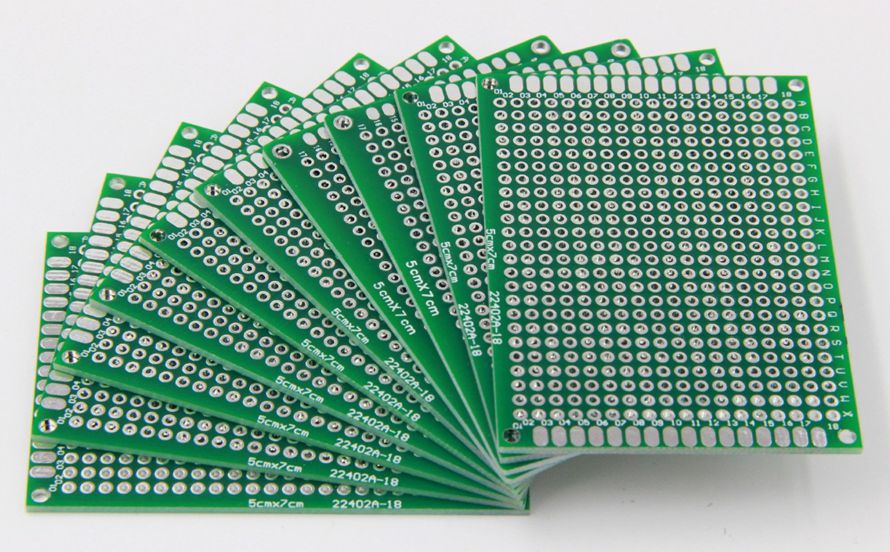
Custom PCB Prototype Germany Services We Offer
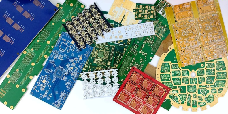
- Rigid PCB Prototypes: 2-16 layers, 0.4-7.0mm thickness, HASL/ENIG surface finishes, RoHS compliant.
- Flexible & Semi-Flex Prototypes: Polyimide substrates, precise deep milling, suitable for compact devices.
- HDI PCB Prototypes: Up to 20 layers, blind/buried vias, ideal for high-density electronic products.
- Ceramic PCB Prototypes: High-temperature resistance, 200 W/m·K thermal conductivity for industrial use.
- Metal Core Prototypes: Aluminum/copper core for thermal management in automotive projects.
- RF & Microwave Prototypes: ±5% impedance tolerance, supporting wireless communication devices.
Our Quality Standards for Prototype PCB
- Material Compliance & Grade Assurance: All substrates are 100% RoHS 2.0 compliant, adhering to restrictions on 11 hazardous substances (each ≤0.1%). We follow IPC-A-600 Class 2 and Class 3 standards — Class 2 for general electronics with acceptable minor defects, and Class 3 for high-reliability PCB prototype Germany in medical/automotive sectors (zero critical defects). This ensures smooth European market certification and avoids compliance delays.
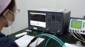
- Full-Coverage Electrical Testing: Every prototype undergoes 100% electrical testing via Keysight E4980A LCR meters. We verify continuity, insulation resistance (>10?Ω at 500V DC) and impedance (±5% tolerance for 50Ω/75Ω standards). Ansys SIwave pre-production simulation identifies signal integrity risks upfront, cutting rework costs by up to 40%.
- High-Precision Visual & Automated Inspection: AOI inspection uses Koh Young Zenith 3D equipment (20μm resolution, 30cm?/sec speed) to detect soldering bridges, component offset (≤0.05mm), surface scratches (<0.1mm) and solder paste inconsistencies. Critical prototype PCB Germany for medical use gets 100% manual recheck by senior technicians (5+ years of experience), achieving 99.9% defect detection.
- Premium Substrate & Traceability: We standardize on halogen-free high-Tg (≥170℃) substrates (Panasonic R-1766, Nanya NE-160A) and offer AlN ceramic substrates (200 W/m·K thermal conductivity) for high-heat needs. Each batch has manufacturer certification, with MES system tracking substrate lot numbers, production timelines and test data for full traceability.
- Industrial-Grade Environmental Validation: Prototypes undergo IPC-6012/2221 testing, including 1000 cycles of temperature cycling (-40℃ to 125℃ at 5℃/min) and 1000 hours of 85℃/85%RH humidity aging. Post-test inspection confirms substrate warpage (≤0.2%) and impedance drift (<3%), ensuring stability for PCB prototyping Germany in harsh environments.
Our Lead Time for Germany PCB Prototyping
| Layers | Normal Service | Fastest Service |
| 1 | 7 Days | 24 H |
| 2 | 8 Days | 24 H |
| 4 | 10 Days | 48 H |
| 6 | 10 Days | 72 H |
| 8 | 12 Days | 72 H |
| ≥10 | TBD | TBD |
Case Studies of Our Medical PCB Prototyping Germany
Project Background: A German medium-sized professional medical device manufacturer needed prototyping PCB Germany for a portable blood glucose monitor, designed for outpatient rapid testing. The project demanded extreme reliability to avoid misdiagnosis risks and strict compliance with European medical device regulations.
Project Requirements: 6-layer HDI PCB with 0.15mm microvias (blind-buried via interleaving layout), biocompatible ENIG finish (nickel layer 50-100 microinches, gold layer 2-5 microinches), ISO 13485 compliance covering design control and material traceability, and 5-day delivery to meet clinical trial scheduling.
Project Challenges: The 5-day timeline clashed with complex HDI blind-buried via layout; biocompatibility required zero sensitization risk for skin-contact areas; 99.9% electrical reliability mandated signal stability under frequent outpatient use; and full material traceability was needed for ISO 13485 audit.
Our Solutions: Leveraging our PCB prototype Germany expertise, we activated MES system’s medical emergency order channel to prioritize production and sync progress in real time. We adopted medical-grade ENIG materials and Panasonic R-1766 high-Tg substrate, conducted 3 rounds of impedance testing with Keysight E4980A (±5% tolerance), and assigned a team of HDI specialists and medical PCB auditors for full-process coordination.
Output Results: Delivered 50 prototypes in 4 days (20% faster than required) with 99.92% yield rate. All units passed biocompatibility testing and ISO 13485 audit. The client completed clinical trials on schedule, with feedback noting “prototypes maintain signal stability in 1000+ consecutive tests, meeting medical precision demands,” and signed a 3-year contract with annual PCB prototype Germany supply exceeding 500 units.
FAQs of PCB Prototyping Germany
Q1: How to avoid narrow drilling breakage in PCB prototype design?
A1: Adopt high-mechanical-strength substrates like Panasonic high-Tg materials and precision drilling equipment with ±0.01mm tolerance. We support 0.1mm drill sizes for PCB prototype Germany, complemented by 100% plated-through hole inspection to ensure conductivity and eliminate breakage risks.
Q2: What causes inconsistent surface finishes in prototype PCBs?
A2: Inconsistencies arise from improper material storage or uneven plating current. Our process uses climate-controlled storage and automated plating systems, delivering uniform HASL/ENIG finishes for all PCB prototyping Germany orders with 100% visual inspection and AOI verification.
Q3: Can via-filling be added to rapid PCB prototyping orders?
A3: Yes. We provide epoxy via-filling (conductive/non-conductive) for rapid prototyping PCB Germany, which boosts structural stability. This service is available for 24-hour expedited orders without extending lead time, aligning with tight project schedules.
Q4: How to resolve impedance control deviations in high-frequency prototypes?
A4: Optimize trace width and spacing via 3D field simulation tools, paired with precision etching (±5% tolerance). For PCB prototype Germany, we conduct pre-production impedance testing with Keysight equipment and adjust designs to meet 50Ω/75Ω standard values, ensuring signal integrity.
Q5: Why does substrate warpage occur in high-temperature PCB prototypes?
A5: Warpage results from mismatched thermal expansion coefficients of substrate materials and inadequate curing processes. For PCB prototype Germany, we use high-Tg (≥170℃) substrates and precise thermal curing control, followed by post-production flatness testing (≤0.2% warpage) to ensure stability in high-temperature scenarios.