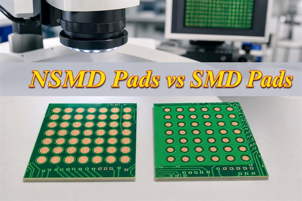
An NSMD pad is a copper land whose edge remains exposed because the solder mask opening is larger than the pad. Solder can wet the pad top and sidewall, which often improves solder-joint compliance and creates more routing room around a BGA. The choice between NSMD and solder mask-defined pads still depends on the component land pattern, ball pitch, mask capability, mechanical loading and assembly process.
This article explains the geometry behind both pad types, their practical trade-offs, and the design-to-inspection controls needed for reliable BGA assembly. It supports PCB layout, DFM, fabrication, assembly and quality decisions but does not replace the component manufacturer’s recommended land pattern.
What Is an NSMD Pad?
NSMD means non-solder mask-defined: the copper feature, rather than the mask opening, defines the solderable land. The mask is pulled back from the copper perimeter, leaving a clearance ring. During reflow, molten solder can contact the pad surface and exposed copper sidewall.
The alternative is an SMD, or solder mask-defined, pad. Its copper land is larger than the mask opening, so the solder mask overlaps the copper edge. Only the area inside the opening is intentionally exposed. “SMD” in this context describes the pad geometry; it should not be confused with the broader term “surface-mount device.”
An NSMD pad is also called a copper-defined pad or metal-defined pad. These names describe the same controlling relationship: the finished copper diameter or outline establishes the land size. That makes copper imaging and etching accuracy central to the result, while mask registration and minimum mask web still determine whether the planned clearance can be produced consistently.
Judge the geometry on the finished board, not only in the EDA library. The NSMD pad library diameter is an artwork target; the solder joint forms on the copper left after imaging, plating and etching. An undersized finished land loses solderable and bonded area, while an oversized land reduces routing and mask clearance.
The mask does not define the land diameter, but it still controls clearance around the copper perimeter and the remaining web between adjacent openings. A complete NSMD pad specification therefore connects copper diameter, mask opening, pitch, registration tolerance and finished mask dam. The name alone does not establish a manufacturable geometry.
Start with the current BGA land-pattern recommendation. Check any footprint change against ball diameter, package collapse, stencil design, board construction and mechanical loading. NSMD describes the geometry; it does not validate one land size for every component.
What Are the Advantages and Disadvantages of NSMD Pads?
NSMD pad geometry offers sidewall wetting, routing flexibility and favorable solder-joint geometry, but it provides less mask overlap to anchor the copper land. Its value is therefore strongest when the footprint, board construction and expected mechanical loads are evaluated together.
Advantages of NSMD Pads
- More solderable surface: Solder can wet the top and sides of the exposed land, providing more wetted interface area than is available through a top-only opening of the same nominal diameter.
- Improved routing space: A smaller copper land may leave more room for escape traces between BGA pads, particularly where pitch and layer count make fan-out difficult.
- Reduced mask-edge constraint: The solder joint is not formed against a mask edge over the copper, which can reduce stress concentration in some thermal-cycling conditions.
- Better copper control: Copper feature location and size are generally controlled more tightly than solder mask registration, making the copper-defined land useful when repeatable pad geometry is required.
Disadvantages of NSMD Pads
Sidewall wetting forms solder around a defined copper feature, while a smaller land can release routing width. Both benefits depend on repeatable finished copper and stable paste transfer.
- Pad-lift sensitivity: Because the mask does not overlap the pad edge, the land has less supplemental restraint during rework, board bending, drop or connector-induced loading.
- Mask-web constraints: Fine pitch may leave too little solder mask between adjacent openings. A broken or missing dam can change paste and solder behavior.
- Etch dependence: Over-etching reduces pad diameter and annular copper area; under-etching narrows routing clearance and alters solder volume.
- No universal default: Certain packages, pitches or mechanical environments may favor SMD pads, mixed strategies approved by the component supplier, or a package-specific land pattern.
The disadvantages become more important as pitch decreases. Larger mask openings reduce the web between adjacent pads, while smaller copper lands leave less bonded area to resist peeling during rework or board flex. The design must balance routing access and solder wetting against mask manufacturability and land retention, rather than selecting NSMD from a generic preference.
Control these risks in both data sets: fabrication documents define finished copper and mask limits, while assembly documents control the stencil, paste, reflow and repair limits.
What Is the Difference Between SMD and NSMD Pads?
NSMD pad size is controlled by copper, while SMD pad size is controlled by the solder mask opening. This single geometric distinction changes sidewall wetting, paste containment, routing room, copper retention, registration sensitivity and the way strain reaches the solder joint.
| Comparison Dimension | NSMD Pad | SMD Pad |
| Defining feature | Finished copper land | Solder mask opening |
| Mask-to-copper relationship | Opening larger than copper pad | Opening smaller than copper pad |
| Exposed copper | Pad top and perimeter sidewall | Pad top inside the mask aperture |
| Solder containment | Less constrained by the mask edge | Mask aperture confines the exposed area |
| Copper pad retention | No mask overlap at the pad edge | Mask overlaps the copper perimeter |
| Thermal-fatigue behavior | Often favorable because of sidewall wetting and joint compliance | Mask edge can create a different strain concentration |
| Escape-routing room | Usually greater for the same pitch | Larger copper land may consume more channel width |
| Copper fabrication sensitivity | High; finished copper sets land size | Moderate; copper must remain beneath the mask overlap |
| Mask registration sensitivity | Clearance must remain around the entire pad | Aperture location sets the exposed land |
| Fine-pitch mask web | May become too narrow between enlarged openings | Can preserve a mask-defined aperture but still needs a manufacturable dam |
| Typical selection driver | BGA reliability, sidewall wetting and routing density | Pad anchoring, paste control or package-specific requirements |
| Primary failure concern | Pad lift, insufficient mask web or undersized etched land | Mask-edge stress, misregistered aperture or reduced exposed area |
Nominal diameter alone cannot decide between the two. NSMD places more control on copper fabrication; SMD places more on mask aperture placement. Compare them with the same package, pitch, copper thickness, finish, stencil and loading condition, then identify the process with the smallest remaining margin.
When Should NSMD Pads Be Used or Avoided?
Use NSMD pads when the component land pattern supports them and the design benefits from sidewall wetting or tighter BGA escape routing. Avoid treating them as a universal rule, especially when mask dams, pad adhesion or severe mechanical loading dominate the risk.
When to Use NSMD Pads
- Use for recommended BGA footprints: Apply NSMD when the component supplier specifies a copper-defined land and provides compatible copper and mask dimensions.
- Use for routing-limited arrays: Consider NSMD when smaller lands provide a viable channel for fan-out without violating trace, space or via constraints.
- Use for thermal-cycling priorities: Evaluate NSMD where joint compliance and sidewall wetting may improve fatigue performance under the project’s verified temperature profile.
- Use with capable fabrication: Confirm finished copper tolerance, mask registration and minimum dam before relying on a narrow clearance window.
Calculate the finished routing channel and mask dam with the selected fabricator’s tolerances. If they pass only at nominal values, the layout has no production margin.
When to Avoid NSMD Pads
- Avoid unsupported footprint changes: Do not convert an SMD recommendation to NSMD only to gain routing space without package-level review.
- Avoid marginal mask webs: If the calculated dam is below the fabricator’s finished capability after registration tolerance, redesign the opening strategy.
- Avoid unverified high-strain use: Drop, board bend, repeated connector loading and aggressive rework can make pad adhesion the limiting failure mode.
- Avoid blind mixed definitions: Mixing SMD and NSMD under one component can create unequal stand-off or strain unless the package manufacturer explicitly uses that pattern.
Avoidance does not always require converting the entire array. Use a mixed pattern only when qualified package guidance specifies it; an improvised pattern can change local stand-off and strain.
How Should NSMD Pads Be Designed for Reliable BGA Solder Joints?
Design the land, mask opening, escape routing and assembly process as one controlled system. Use the following sequence.
- Confirm the package land pattern. Record ball pitch, ball diameter, copper land, mask opening and pad definition from the current component drawing. Check the revision and whether the dimensions apply to the PCB land, package substrate or stencil. Do not scale a generic footprint when package-specific guidance is available.
- Define the service loads. List the required thermal range, cycle count, vibration, drop, board bending and permitted rework exposure. Identify whether solder fatigue, copper-pad retention, package warpage or enclosure strain is most likely to limit reliability.
- Select the escape structure. Choose dog-bone fan-out, blind microvias or via-in-pad from the pitch, I/O count and finished routing rules. Include neck-down length, via annular ring, plane clearances and the layer transitions needed to reach inner routing layers.
- Set copper and mask limits. Keep clearance around the finished copper pad while preserving the fabricator’s minimum finished mask dam. State the target, tolerance and inspection point for both features so nominal CAD values are not mistaken for finished acceptance limits.
- Coordinate paste and reflow. Match the stencil aperture and paste volume to the land, via structure, component and reflow profile. Review aperture reduction, stencil thickness, paste release, via-cap planarity and package collapse together because each affects final solder volume.
- Verify before production. Inspect Gerber or ODB++, complete fabrication and assembly DFM, and approve representative hardware by solder paste inspection, X-ray and electrical test. Where service risk justifies it, add cross-section, bend, thermal-cycle or daisy-chain validation with written acceptance criteria.
Release a controlled NSMD pad record that links the package drawing, copper and mask data, fabrication tolerances, stencil revision and inspection plan. Do not rely on the EDA library name alone.
How Should NSMD Pad Size, Solder Mask Expansion and Spacing Be Set?
Set NSMD geometry from the component land pattern, then prove that the worst-case finished mask opening still clears the copper pad and leaves a producible dam. A nominal clearance that looks correct in CAD can disappear after copper and mask tolerances are applied.
- Fix the finished copper target. Use the package supplier’s land diameter or a qualified project value. State whether the number is a CAD target, artwork diameter or finished acceptance dimension. If CAM applies etch compensation, retain both the released artwork value and the required finished result.
- Add radial mask clearance. For a circular NSMD pad, nominal mask opening diameter equals copper pad diameter plus twice the radial expansion. A 0.30 mm copper pad with 0.05 mm expansion per side produces a 0.40 mm nominal opening; this is an example, not a universal recommendation.
- Calculate the nominal mask dam. For equal circular pads on pitch P, the nominal dam between openings is P − opening diameter. At 0.50 mm pitch with a 0.40 mm opening, the nominal dam is 0.10 mm before process allowances.
- Apply the tolerance stack. Subtract the relevant copper-size variation, mask-opening variation and relative registration allowance using the fabricator’s stated method. Confirm whether tolerances are radial, diametric, unilateral or positional. Registration is positional, so treating it as a simple diameter tolerance can understate worst-side clearance.
- Check trace and via clearances. The finished copper pad must preserve spacing to escape traces, dog-bone vias, filled microvias and adjacent nets after etch compensation. Review array corners and neck-down transitions, not only the repeating center cell.
- Resolve conflicts through DFM. If the mask dam or routing channel fails at worst case, consider a supplier-approved gang opening, revised pad definition, qualified narrow routing, via-in-pad, buildup changes or a different escape strategy. Record the exception so it is not lost during a later CAM or supplier change.
The drawing should identify the controlling dimensions and acceptance method. Without that distinction, the library value, plotted artwork and finished board measurement may be compared as if they were the same object.
Check three finished conditions: smallest copper land, largest copper land and maximum mask shift. They test bonded area, routing clearance and worst-side mask encroachment, respectively.
How Do Copper Etching and Solder Mask Registration Tolerances Affect NSMD Pads?
Copper etching changes the land that defines an NSMD pad, while mask registration changes the clearance around it. Their combined effect can produce an undersized pad, uneven exposed sidewall, insufficient dam or local mask encroachment even when nominal data are correct.
- Over-etching: Reduces finished pad diameter, solderable area and pad-to-laminate bond area. It may also alter paste-to-pad area ratio.
- Under-etching: Enlarges the pad, reduces routing clearance and consumes part of the planned mask pullback.
- Mask shift: Creates unequal radial clearance. Severe shift can expose excess laminate on one side and approach or cover copper on the other.
- Opening variation: Changes the mask dam between neighboring BGA lands and may convert separate openings into an unintended broken web.
- Layer-to-layer scaling: Panel movement and imaging compensation can affect copper-to-mask alignment across a large array or panel.
DFM should therefore report both the nominal geometry and the predicted finished condition. Useful controls include artwork compensation, solder mask registration targets, minimum finished dam, coupon or sample measurements, and a clear escalation rule when the array cannot meet all limits simultaneously.
Sample NSMD pad measurements across the panel; one array can miss scaling or positional trends. Agree on the measurement method, magnification, sample size and limits before fabrication.
Match the correction to the cause. A larger mask opening may remove encroachment but break the dam; larger copper artwork may recover an over-etched land but narrow the routing channel. Recheck both copper and mask before releasing revised data.

How Do NSMD Pads Affect BGA Fan-Out, Via-in-Pad and Stencil Design?
Smaller copper lands can create more routing room, but the via and stencil must still support stable solder volume. Check the design in this order.
- Choose the fan-out method. Use dog-bone escape where the finished channel fits; use blind microvias or via-in-pad when it does not. Include breakout direction and layer assignment because a solution for the outer rows may block inner power or ground connections.
- Check finished copper spacing. Verify pad-to-trace, trace-to-trace, neck-down and annular-ring dimensions after etch compensation. Use the smallest finished spacing, not the nominal CAD gap, as the DFM decision value.
- Control via-in-pad construction. Specify filling, capping and planarization so the via cannot wick solder or leave an unacceptable surface depression. Define via type, fill material, cap requirement and permitted surface condition; an open or partially filled via can remove solder from the joint.
- Set the stencil aperture. Match aperture area, shape and stencil thickness to the required paste volume instead of applying a universal one-to-one opening. Review area ratio, neighboring components and any stepped-stencil need so the BGA aperture does not create a print conflict elsewhere.
- Validate the assembled array. Correlate paste inspection and X-ray results with via location, stencil aperture and reflow settings before volume release. Compare edge, corner and center balls because temperature, warpage and collapse can differ across a large package.
Keep NSMD pad fan-out, via and stencil revisions linked. A late via-in-pad or copper-compensation change can alter paste loss, joint volume and routing clearance, so review PCB data, stencil data and assembly criteria together.
Which NSMD Pad Defects Can Occur During PCB Fabrication and Assembly?
NSMD defects arise from copper geometry, mask alignment, surface condition, paste transfer, reflow and mechanical loading. Finding the process stage that created the defect is more useful than labeling every BGA failure as a “pad problem.”
| Defect | Likely Mechanism | Observable Evidence | Corrective Direction |
| Undersized copper land | Excessive etch or incorrect compensation | Optical measurement below finished requirement | Correct artwork compensation and monitor finished pad size. |
| Mask encroachment | Registration shift or undersized opening | Unequal clearance or mask touching copper | Adjust opening, alignment controls or footprint strategy. |
| Broken mask dam | Nominal web too narrow for process capability | Missing or discontinuous mask between pads | Revise openings or use an approved gang-mask approach. |
| Insufficient solder joint | Low paste transfer, via wicking or poor wetting | Open circuit, reduced joint volume or X-ray anomaly | Review stencil, via fill, surface condition and reflow profile. |
| Bridge | Excess paste, missing dam, placement error or collapse | Electrical short or connected features on X-ray | Correct aperture, mask geometry, placement and reflow conditions. |
| Void concentration | Via-in-pad, trapped volatiles or unsuitable reflow behavior | X-ray voids located near via or joint interface | Improve via filling, paste selection, aperture and thermal profile. |
| Pad lift | Rework heat, board bend, impact or low copper adhesion area | Land separates from laminate, often with an open circuit | Reduce mechanical and thermal strain; review pad definition and rework limits. |
| Intermittent BGA connection | Head-in-pillow, crack, warpage or marginal joint formation | Temperature- or flex-sensitive electrical failure | Correlate X-ray, warpage, reflow, cross-section and electrical evidence. |
An open circuit may come from an undersized land, poor paste transfer, via wicking, head-in-pillow or a post-assembly crack. Preserve evidence from the bare board, print, placement, reflow and handling stages instead of relying on one X-ray image.
Verify each correction with the right output: finished-land measurements for etching, paste-volume data for the stencil, joint evidence for reflow, and strain controls for handling.
How Can NSMD Pad and BGA Solder Joint Quality Be Inspected?
Inspect each NSMD pad on the bare board before verifying paste transfer, hidden joints and electrical performance. Use separate methods for each failure layer.
- Verify released data. Match copper, mask, paste and drill layers to the approved footprint and DFM record. Confirm that CAM compensation, panel scaling and approved mask exceptions are traceable to the correct revision.
- Measure the bare board. Sample finished pad diameter, mask opening, radial clearance and mask dam at multiple panel locations. Record the measurement system and sampling plan so prototype and production results can be compared consistently.
- Check surface and via quality. Inspect finish coverage, contamination, scratches, mask adhesion, via fill, cap and planarity. For via-in-pad, distinguish cosmetic color variation from a depression, void or exposed via that can change paste transfer.
- Inspect solder paste. Use solder paste inspection to identify offset, poor transfer and excessive or insufficient deposits before placement. Trend volume and position across the array instead of judging only whether a deposit is present.
- Examine hidden joints. Use X-ray to assess bridges, opens, solder-volume variation, joint shape and void distribution after reflow. Interpret images against package structure and viewing angle because X-ray does not prove that every interface is bonded.
- Confirm function and failure mode. Apply continuity, boundary-scan or functional testing; use microsection or dye-and-pry only when root-cause evidence requires it. Destructive analysis should answer a defined question and include comparison joints so normal features are not mistaken for failures.
Link every result to the material lot, panel, assembly lot, stencil revision and reflow profile so repeated defects can be traced to a controlled process variable.
Each method has a separate job: optical measurement checks geometry, SPI checks the print, X-ray evaluates hidden features, and electrical testing confirms connectivity or function. Select the combination by package pitch, via structure and product risk.

FAQs About NSMD Pads
Q1: How should bare boards with fine-pitch BGA lands be stored before assembly?
A1: Keep boards sealed, clean and within the approved storage period. Moisture, dust, fingerprints and sulfur-bearing packaging can degrade solderability even when the pad geometry is correct. Define packaging, humidity control, shelf life and any bake decision from the laminate, finish and assembly requirements.
Q2: Are NSMD lands compatible with lead-free solder?
A2: Yes, when the finish, paste and thermal profile are qualified together. Lead-free assembly normally uses higher process temperatures than traditional tin-lead assembly, so package warpage, flux activation, wetting and rework exposure must be evaluated for the actual component and board construction.
Q3: How should BGA rework limits be controlled?
A3: Set a documented maximum number of heating cycles and record every rework event. Repeated heating can weaken copper adhesion, damage mask, oxidize the finish and increase laminate stress. A repaired assembly should pass the same electrical and inspection requirements defined by the approved repair procedure.
Q4: Does PCB thickness influence BGA joint reliability?
A4: Board thickness changes stiffness, bending response and assembly warpage. A thicker board is not automatically safer because local copper balance, component position, depanelization and enclosure loading also matter. Evaluate strain at the BGA location under the product’s real mechanical conditions.
Q5: How does copper thickness affect the finished land diameter?
A5: Thicker copper generally requires more etch compensation to reach the target feature. The fabricator should distinguish the artwork value from the finished measured diameter. Otherwise, the same CAD land can finish differently when copper weight, plating buildup or etching conditions change.
Q6: Can conformal coating be applied over a BGA area?
A6: It can, but coating and keep-out requirements should be defined before assembly. Coating beneath or around a BGA may affect inspection, cleaning, probing and future rework. Specify masking boundaries, coating material, cure conditions and acceptance criteria for the finished product.
Q7: What should be frozen for repeat production orders?
A7: Freeze the approved footprint, Gerber or ODB++, stack-up, material, finish, stencil revision and assembly profile. Require written approval before changes to copper compensation, solder mask, via fill, paste aperture or component revision. This prevents an unnoticed process change from altering the joint geometry.
Q8: When is a daisy-chain test vehicle useful?
A8: Use one when normal functional testing cannot isolate package-interconnect failures. A representative daisy-chain board can support thermal cycling, bend, drop or process-development studies. Its package, pad layout, stack-up and assembly conditions must represent the production design closely enough to make the result relevant.
Q9: Can stencil wear change BGA solder consistency?
A9: Yes; damaged apertures, residue and poor underside cleaning can change paste transfer. Define inspection and cleaning intervals, check aperture condition, and monitor paste results over the production run. Replacing a worn stencil is more reliable than compensating with unapproved print settings.
Q10: Can underfill be used beneath a BGA with NSMD lands?
A10: Yes, but the underfill process must be qualified for the package and service environment. Material flow, cure temperature, voiding, board warpage and future rework all require review. Underfill can redistribute mechanical strain, so reliability results from an unfilled assembly should not be assumed to remain unchanged.
NSMD pads are most effective when copper geometry, solder mask capability, BGA fan-out, stencil design and inspection criteria are controlled as one manufacturing system. Use the package land pattern as the starting point, test the finished tolerance stack, and validate the assembly against the actual thermal and mechanical loads.
For an NSMD pad or BGA PCB quotation, contact EBest Circuit at sales@bestpcbs.com. Send your Gerber or ODB++ files, BOM, stack-up, BGA package information, quantity, assembly requirements and test plan so our team can review manufacturability and prepare an accurate quotation.