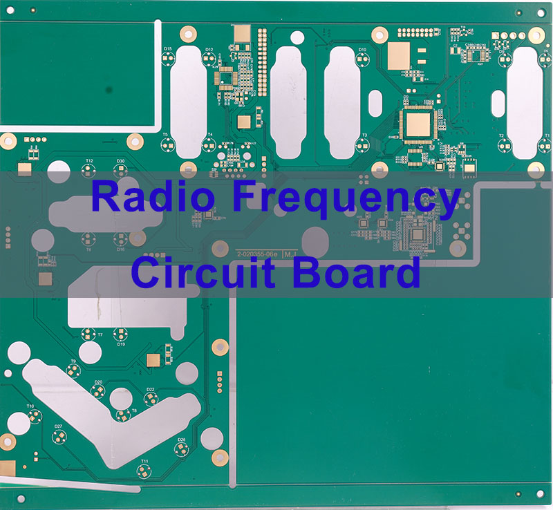
A 50-ohm RF PCB can still show more RF insertion loss than its design allows. At 6 GHz, an S21 reading of -3 dB means only about half the incident power reaches a matched output. The problem may come from the laminate, copper roughness, excessive trace length, or poorly matched transitions.
Before selecting a low‑loss material or approving a stackup, it helps to know where RF insertion loss comes from and how much the signal path can tolerate. This guide covers the main causes, VNA measurement methods, acceptable loss limits, and practical ways to reduce attenuation before PCB manufacturing.
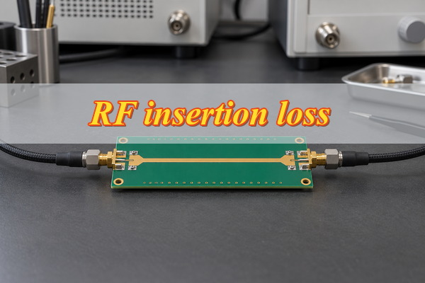
What Is Insertion Loss in RF?
RF insertion loss is the reduction in signal power transmitted through an RF path, expressed in decibels (dB). In a PCB, this path may include copper traces, vias, connectors, and transmission‑line transitions.
Insertion loss is commonly calculated from the forward transmission parameter S21:
Insertion Loss (dB) = -20 log10(|S21|)
For example, an S21 reading of -3 dB corresponds to approximately 50% power transmission into a matched output. The remaining power may be dissipated, reflected, or radiated, depending on the RF structure.
Lower insertion loss generally means more signal power reaches the intended destination.
What Is the Difference Between Insertion Loss and Return Loss?
Insertion loss measures signal attenuation through an RF path, while return loss measures reflected signal power caused by impedance mismatches. Both are expressed in decibels but evaluate different aspects of RF transmission.
| Parameter | Insertion Loss | Return Loss |
|---|---|---|
| S‑Parameter | S21 | S11 |
| Measurement | Forward transmission | Input reflection |
| Formula | -20 log10(abs(S21)) | -20 log10(abs(S11)) |
| Main Purpose | Evaluate signal attenuation | Evaluate impedance matching |
| VNA Reading | S21 typically negative in dB for a passive attenuating path | S11 typically negative in dB |
| Preferred Result | Lower positive loss | Higher positive return loss |
| Example | S21 = -1 dB means 1 dB insertion loss | S11 = -20 dB means 20 dB return loss |
The return‑loss measurement assumes the other VNA port is terminated in the reference impedance.
For example, 20 dB return loss indicates approximately 1% reflected power, but good impedance matching does not guarantee low insertion loss. A long transmission line can still lose significant energy through conductor and dielectric attenuation.
S21 and S11 should be evaluated together to distinguish transmission attenuation from reflection‑related problems.
What Causes RF Insertion Loss in a PCB?
RF insertion loss in PCBs mainly comes from conductor resistance, dielectric dissipation, radiation or leakage, and impedance discontinuities. Their effects become more noticeable as operating frequency increases.
- Conductor Loss: Skin effect concentrates high‑frequency current near the copper surface, increasing effective resistance. Rough copper surfaces can contribute additional attenuation.
- Dielectric Loss: Electromagnetic energy is dissipated within the PCB insulating material. Higher dissipation factors generally produce greater dielectric attenuation under comparable conditions.
- Radiation and Leakage: Discontinuous reference planes, unsuitable transitions, and poorly contained electromagnetic fields may allow energy to escape the intended signal path.
- Impedance Mismatch: Variations in trace geometry, connector launches, or via structures create reflections and reduce measured forward transmission.
Conductor and dielectric losses typically increase with frequency, while impedance discontinuities can create ripples or sharp dips in the S21 curve.
If the measured S21 response contains sudden fluctuations, inspect the connector transitions, vias, and test fixture before attributing the problem to PCB materials.
How Do PCB Materials Affect RF Insertion Loss?
PCB materials influence RF insertion loss through dielectric properties, copper roughness, and environmental stability. Dissipation factor (Df) is a primary indicator of dielectric attenuation, while dielectric constant (Dk) affects transmission‑line impedance and electrical length.
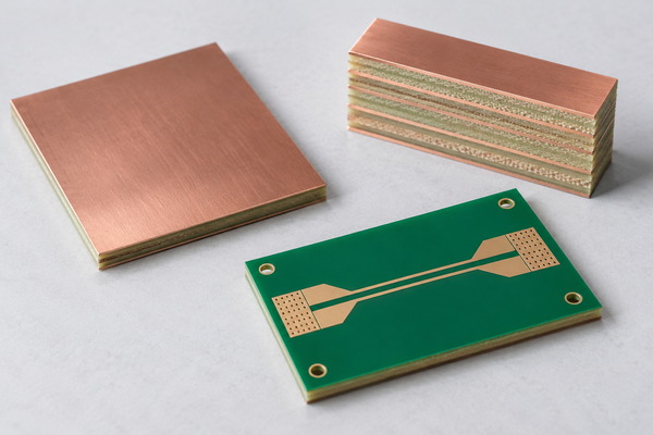
| Material Property | Effect on RF Performance | Selection Consideration |
|---|---|---|
| Dissipation Factor (Df) | Higher Df increases dielectric loss | Low Df at operating frequency |
| Dielectric Constant (Dk) | Affects impedance and signal propagation | Stable Dk and controlled tolerance |
| Copper Roughness | Increases conductor attenuation | Suitable low‑profile copper |
| Dielectric Thickness | Changes transmission‑line geometry | Controlled thickness tolerance |
| Moisture Absorption | May alter dielectric properties | Stable performance in service |
| Thermal Stability | Influences RF properties across temperature | Suitable operating temperature range |
Standard FR-4 may be adequate for shorter RF paths with moderate insertion‑loss requirements. For longer routes or demanding microwave applications, low‑loss laminates may provide better attenuation performance.
For reference, Rogers material data lists the following typical dissipation factors at 10 GHz:
| Material | Df at 10 GHz | Typical Application Consideration |
|---|---|---|
| RO4003C | 0.0027 | Low‑loss microwave transmission lines |
| RO4350B | 0.0037 | RF circuits requiring low loss and UL 94 V-0 flame resistance |
These figures describe material properties, not the insertion loss of a finished PCB. Actual attenuation also depends on copper roughness, trace geometry, dielectric thickness, and operating conditions.
Material selection should be based on the required RF loss budget rather than Df alone. Compare candidate laminates using equivalent transmission‑line structures and supplier data at the intended operating frequency.
How Do Frequency, Trace Length, and PCB Stackup Affect RF Insertion Loss?
RF insertion loss generally increases with frequency and transmission‑line length, while PCB stackup determines how electromagnetic fields interact with the dielectric and copper conductors.
Frequency: As frequency rises, skin effect increases conductor resistance, while dielectric attenuation typically becomes more significant. Copper roughness can further increase high‑frequency losses.
Trace Length: Longer transmission lines accumulate more attenuation. For a uniform, well‑matched structure, insertion loss in dB increases approximately in proportion to length. This relationship allows engineers to estimate attenuation in dB/in or dB/cm.
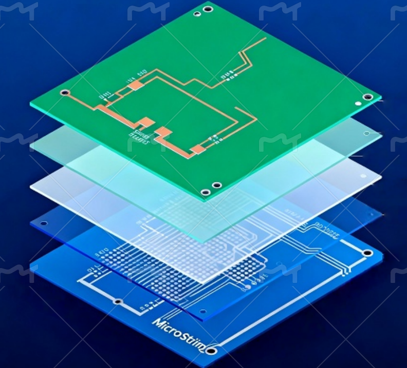
PCB Stackup: Microstrip and stripline structures distribute electromagnetic fields differently. Microstrip fields extend partly into air, potentially reducing dielectric attenuation, while stripline offers stronger field containment and shielding.
The stackup also controls impedance through dielectric thickness, trace dimensions, and reference‑plane geometry. Poorly controlled dimensions can introduce mismatches that increase measured RF insertion loss.
Choose the transmission‑line structure according to the operating frequency, impedance target, routing requirements, and available loss budget.
How Do You Measure RF Insertion Loss Using a VNA?
RF insertion loss is commonly measured using a vector network analyzer (VNA), which records S21 across the specified frequency range. Keysight’s S‑parameter overview identifies S21 as forward transmission and explains that calibration establishes the measurement reference plane. Accurate results still depend on the test fixtures, connector quality, and selected reference‑plane locations.
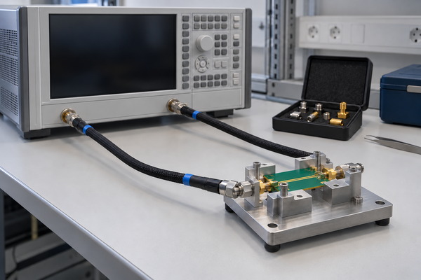
A typical measurement follows five steps.
Step 1: Prepare the Test Setup
Connect the PCB transmission path between VNA Port 1 and Port 2 using suitable RF cables, connectors, or fixtures. Configure the operating frequency range and reference impedance, commonly 50 ohms.
For trace characterization, use a test coupon representing the PCB stackup and transmission‑line geometry.
Step 2: Calibrate the VNA
Perform an appropriate calibration, such as SOLT (Short‑Open‑Load‑Thru) or TRL (Thru‑Reflect‑Line).
Calibration corrects systematic measurement errors and establishes the reference planes. Connector launches and fixtures beyond those planes may still contribute additional loss.
Step 3: Measure S21
Sweep the required frequency range and record the S21 response.
For example, S21 = -1.2 dB at 6 GHz corresponds to 1.2 dB insertion loss under the specified reference conditions.
Check S11 alongside S21 to identify potential impedance mismatches.
Step 4: Account for Fixture Losses
When measuring the PCB transmission line independently, apply a validated de‑embedding method or suitable reference structures to account for connector and fixture contributions.
Avoid subtracting assumed fixture losses without supporting measurements.
Step 5: Verify the Results
Repeat critical measurements where necessary and record the frequency range, calibration method, reference planes, and S21 readings.
A consistent measurement procedure is essential when comparing prototype and production RF PCB performance.
What Is an Acceptable RF Insertion Loss Value for RF PCBs?
There is no universal acceptable RF insertion loss value for every PCB. The maximum permitted loss depends on operating frequency, signal‑path length, receiver sensitivity, available gain, and the RF link budget.
A practical specification defines the maximum attenuation across the required operating band.
Consider an illustrative RF channel with the following requirements:
- Operating Frequency: 6 GHz
- Maximum Channel Insertion Loss: 1.0 dB
- Input Launch Loss: 0.15 dB
- Output Launch Loss: 0.15 dB
- Transmission‑Line Length: 4 inches
Assuming sufficiently good impedance matching:
Available Trace Loss = 1.0 – 0.15 – 0.15 = 0.70 dB
Maximum Average Trace Attenuation = 0.70 / 4 = 0.175 dB/in
This preliminary budget leaves 0.70 dB for the transmission line. Actual measurements must also consider mismatch effects, fabrication variation, and measurement uncertainty.
Specify the maximum insertion loss, operating frequency range, measurement reference planes, and acceptance method before PCB fabrication. A board that passes at one frequency may exceed its loss limit elsewhere in the operating band.
How Can You Reduce RF Insertion Loss in PCB Design?
Reducing RF insertion loss involves controlling conductor and dielectric attenuation while minimizing impedance discontinuities. The following measures can improve transmission performance without unnecessarily increasing PCB manufacturing costs.
- Select Low‑Loss Materials: Choose laminates with suitable Df values at the operating frequency. Compare their performance, availability, and manufacturing requirements.
- Shorten Critical RF Traces: Reduce unnecessary routing length and avoid detours that increase attenuation.
- Maintain Controlled Impedance: Use consistent trace geometry, dielectric thickness, and reference‑plane structures to limit reflections.
- Optimize Copper Characteristics: Review copper roughness, conductor width, and thickness while maintaining the required impedance.
- Minimize Via Transitions: Avoid unnecessary layer changes and review via stub effects, antipads, and return‑path connections.
- Maintain Continuous Reference Planes: Avoid routing critical RF signals across plane splits or poorly controlled return paths.
- Review Surface Finish: Consider finish‑related attenuation where high‑frequency current flows through exposed conductors, particularly with nickel‑containing finishes.
- Verify Before Production: Use simulation, impedance coupons, and agreed S21 measurements to check critical RF transmission requirements.
Low RF insertion loss depends on the complete transmission path, not only the PCB laminate. Appropriate materials, controlled geometry, and well‑designed transitions should be evaluated together.
How Can EBest Circuit Support Low‑Loss RF PCB Manufacturing?
EBest Circuit provides custom RF PCB manufacturing, material guidance, stackup review, and DFM support for high‑frequency applications. We help customers identify fabrication risks that may affect impedance consistency, RF performance, and production costs.
Our manufacturing support focuses on the practical requirements of your project:
- Choose Suitable RF Materials: Compare available FR-4, low‑loss laminates, and hybrid stackups to meet electrical requirements without unnecessary material costs.
- Reduce Manufacturing Risks: Review stackup thickness, copper specifications, trace geometry, and tolerances before production to identify potential fabrication issues.
- Maintain Impedance Consistency: Manufacture to agreed controlled‑impedance specifications and verify relevant parameters according to the approved inspection plan.
- Move from Prototype to Production: Support prototype validation, small‑batch orders, and volume manufacturing while maintaining agreed fabrication requirements.
- Improve Quality Visibility: Provide inspection and production traceability records, with project‑specific testing requirements confirmed before manufacturing.
- Access Technical Guidance: Work through one sales contact with support from a three‑engineer technical team for manufacturability review, process support, and quality coordination.
At EBest Circuit, we manufacture customer‑provided PCB designs and provide DFM guidance rather than original circuit design services.
FAQs About RF Insertion Loss
Q1: Why does a VNA display negative S21 values?
A1: A VNA expresses S21 magnitude in dB. For a passive attenuating path, the reading is negative because the transmitted signal is smaller than the incident signal. S21 = -2 dB corresponds to 2 dB insertion loss.
Q2: What causes ripples in an RF PCB S21 curve?
A2: Ripples often result from reflections between impedance discontinuities, including connector launches, vias, and trace transitions. Check S11 and fixture calibration before attributing the behavior to dielectric loss.
Q3: Can PCB transmission loss be expressed in dB per inch?
A3: Yes. Compare the insertion loss of two matched‑structure test coupons with different lengths. Divide the measured loss difference by the length difference to estimate attenuation per inch, provided launch and mismatch effects are controlled.
Q4: Is standard FR-4 suitable for microwave PCBs?
A4: FR-4 may work for short microwave transmission paths with sufficient loss margin. Longer routes or tighter attenuation limits often favor low‑loss materials. Evaluate the actual frequency, path length, and insertion‑loss budget.
Q5: Does lower Dk always reduce insertion loss?
A5: No. Dk mainly affects propagation and transmission‑line geometry, while Df is more directly related to dielectric attenuation. Copper properties and conductor dimensions also influence overall loss.
Q6: Will thicker copper improve RF transmission efficiency?
A6: Not always. Additional copper thickness may reduce resistance, but skin effect limits the benefit at high frequencies. Copper roughness, trace width, and impedance geometry should also be considered.
Q7: Can ENIG increase RF PCB attenuation?
A7: Yes, in certain structures where RF current interacts with the nickel‑containing finish. Review surface‑finish effects on exposed microwave conductors, especially when insertion‑loss margins are tight.
Q8: Should RF PCB designs avoid all vias?
A8: No. Properly designed vias can provide acceptable RF transitions. Long unused stubs, impedance discontinuities, and poor return paths are more concerning than the presence of a via itself.
Q9: Why do different VNAs produce different S21 readings?
A9: Calibration, reference‑plane placement, cables, connectors, and fixture conditions can affect measurements. Use consistent calibration and test configurations before comparing results.
Q10: Does temperature influence RF transmission attenuation?
A10: Yes. Temperature can change copper resistance and dielectric properties. Check laminate performance over the required operating‑temperature range when the design has a narrow loss margin.
Q11: Is individual VNA testing required for every RF PCB?
A11: Not necessarily. Testing depends on application requirements and the agreed inspection plan. RF test coupons, sampling inspections, or individual measurements may be used according to the required assurance level.
Q12: What information should be included in an RF PCB manufacturing RFQ?
A12: Provide Gerber or ODB++ files, operating frequency, stackup, impedance targets, material requirements, and insertion‑loss limits. Include test coupon and S21 acceptance requirements where applicable.
Conclusion
Reducing RF insertion loss starts with the right material, controlled transmission‑line geometry, and a realistic loss budget. VNA measurements help verify whether the PCB meets its RF requirements, while early DFM reviews can identify manufacturing risks before fabrication.
Ready to manufacture your low‑loss RF PCB? EBest Circuit supports custom RF PCB prototypes, customer‑supplied PCB designs, and volume production with technical guidance throughout the process. Send your PCB files, operating frequency, stackup, and insertion‑loss requirements to sales@bestpcbs.com for a manufacturing review and quotation.