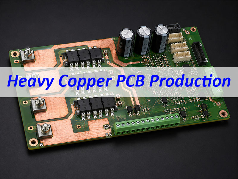
Heavy copper PCB production is used when a printed circuit board must carry higher current, manage heat more effectively, and support stable power delivery in demanding applications. Power boards, motor drive boards, industrial control systems, battery-related circuits, and control and drive PCBs often require thicker copper than standard circuit boards because ordinary copper weight may not provide enough current capacity or thermal robustness.
EBest Circuit (Best Technology) is an engineer-oriented one-stop PCB service provider supporting heavy copper PCB fabrication, DFM review, PCB layout manufacturability feedback, PCBA assembly, testing, and production documentation. For customers developing power or drive boards with thick copper requirements, our role is to help review manufacturability, confirm production feasibility, and support PCB manufacturing and assembly based on customer-provided files. To start a manufacturability review or request a quotation, pls feel free to send your Gerber files and project notes to sales@bestpcbs.com.
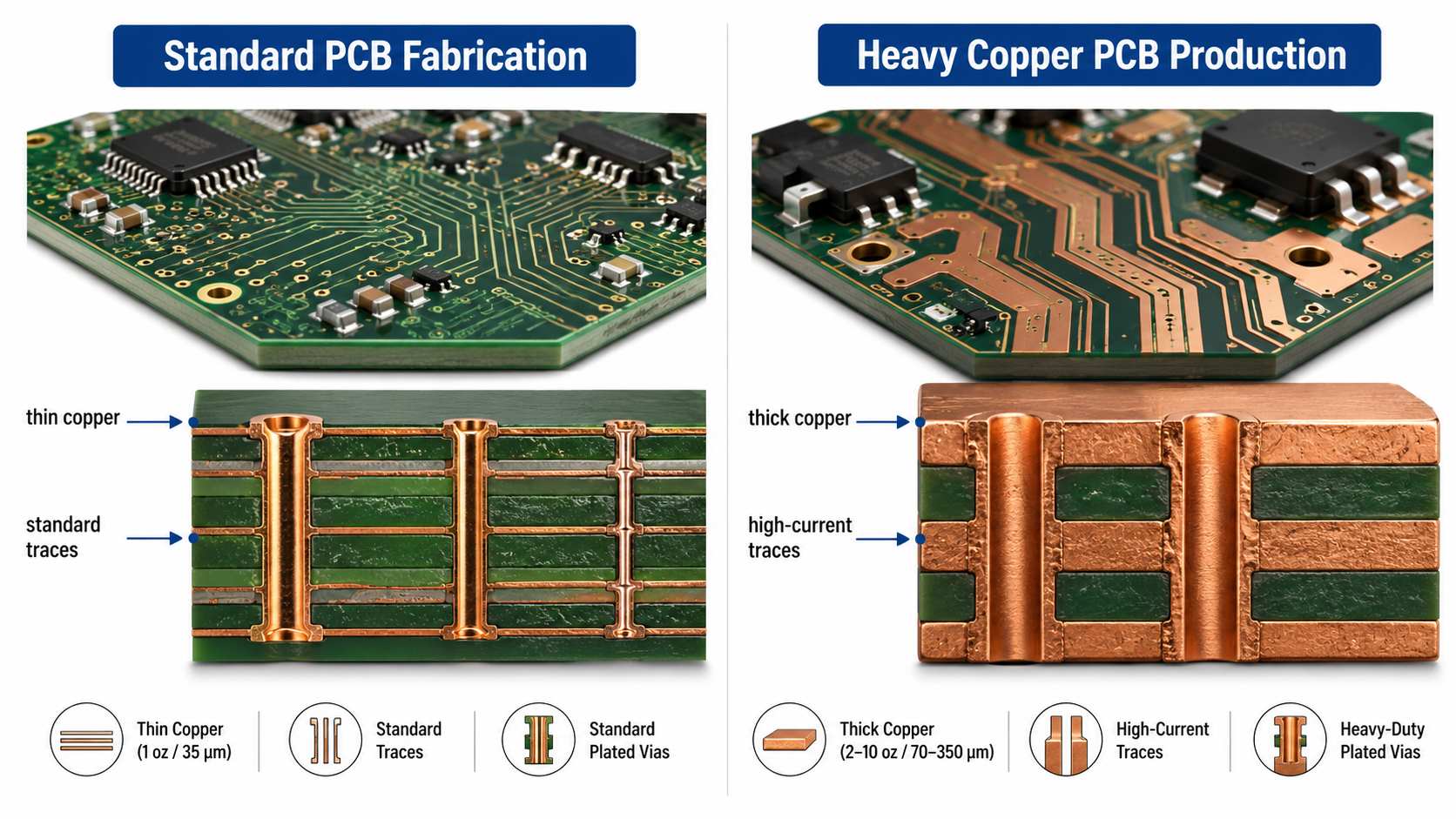
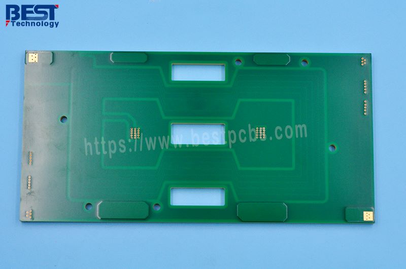
How Is Heavy Copper PCB Production Different from Standard PCB Fabrication?
Heavy copper PCB production is not just standard PCB fabrication with thicker copper added. Once copper weight increases, the process becomes more demanding in etching, plating, spacing, solder mask coverage, lamination, and final inspection.
In standard PCB fabrication, copper is commonly used for signal routing and moderate current paths. In heavy copper PCBs, copper becomes part of the product’s power and thermal strategy.
Key differences include:
- Copper thickness
- Standard PCB copper is often 1 oz or less.
- Heavy copper boards may use 2 oz, 3 oz, 4 oz, or higher copper weight.
- Etching control
- Thicker copper is harder to etch cleanly.
- Line width, spacing, and compensation need closer review.
- Thermal performance
- Heavy copper helps carry current and spread heat.
- Copper distribution must be balanced to reduce warpage risk.
- Solder mask coverage
- Thick copper creates a higher surface profile.
- Solder mask bridging and coverage need careful process control.
- Hole reliability
- Plated holes and vias may carry higher current.
- Hole wall copper quality becomes more important.
- DFM importance
- Gerber files should be reviewed before production.
- Copper spacing, copper balance, hole-to-copper clearance, and solder mask feasibility should be checked early.
For heavy copper PCB production, a competitive price is important, but manufacturability is more important. A board that cannot be reliably produced will create delays, engineering questions, and avoidable cost.
When Does a Drive Board Need Heavy Copper?
A drive board often needs heavy copper when it carries high current, drives motors, controls power stages, or works in an industrial environment where heat and electrical load must be controlled.
Common cases include:
- Motor drive boards
- CNC control and drive boards
- Servo driver boards
- Industrial power control boards
- Battery management support boards
- Inverter and converter PCBs
- Power supply boards
- Automotive power modules
- LED power drive boards
A drive board may need heavy copper when the design has:
- High-current traces
- Power MOSFETs or IGBTs
- Large copper pours
- High thermal load
- Wide power and ground paths
- Connector areas carrying current
- Long operating time under load
- Strict reliability requirements
Heavy copper helps in several ways:
- Reduces conductor resistance
- Helps lower temperature rise
- Improves current-carrying capacity
- Supports stronger power distribution
- Improves mechanical robustness in high-current areas
For a control and drive PCB, the control board may use lighter copper for signal processing, while the drive board may require thicker copper for current handling. This is why each board in a set should be reviewed separately instead of treated as one standard PCB order.
What Copper Weight Is Used in Heavy Copper PCBs?
Copper weight should be selected according to current, heat, trace width, voltage, board size, and manufacturability. There is no single copper thickness that fits every heavy copper PCB project.
Common copper weights include:
| Copper Weight | Typical Use |
|---|---|
| 1 oz | Standard signal and control circuits |
| 2 oz | Moderate current and power boards |
| 3 oz | Higher current paths and power control |
| 4 oz | Heavy copper drive boards and industrial power circuits |
| 5 oz and above | Special high-current applications with engineering review |
Important points:
- Inner copper and outer copper may be different.
A board may use lighter inner copper and heavier outer copper depending on routing and current paths. - Finished copper thickness matters.
Customers should clarify whether copper weight refers to base copper or finished copper after plating. - Thicker copper affects spacing.
As copper becomes thicker, smaller line spacing becomes harder to manufacture. - Thicker copper affects solder mask.
Heavy copper areas need enough solder mask process margin. - Thicker copper affects cost.
Material use, etching time, plating control, and process difficulty all increase.
For power and drive boards, copper weight should be reviewed together with layout manufacturability, board thickness, hole structure, current path, and assembly requirements.
What Manufacturing Challenges Affect Heavy Copper PCB Quality?
Heavy copper PCB quality depends on stable process control. The board may look simple from the outside, but thick copper can create several manufacturing risks if the design is not reviewed properly.
Key challenges include:
- Etching accuracy
- Heavy copper requires more etching compensation.
- Fine traces and tight spacing become harder to maintain.
- Copper spacing
- Insufficient spacing can create production risk.
- High-voltage or high-current areas may need extra clearance.
- Copper balance
- Uneven copper distribution may lead to warpage.
- Large copper areas should be reviewed before production.
- Plating reliability
- Through-hole copper must remain stable.
- Vias in high-current paths need careful review.
- Solder mask process
- Thick copper height can affect solder mask coverage.
- Solder mask bridges may be difficult in dense areas.
- Lamination and board thickness
- Heavy copper changes the final board profile.
- Pressing and resin flow need process control.
- Assembly compatibility
- Heavy copper areas may absorb more heat during soldering.
- Reflow profile and solderability should be considered for PCBA projects.
- Inspection
- AOI, electrical test, and visual inspection are important.
- Cross-section or copper thickness report may be required for some projects.
A reliable heavy copper PCB manufacturer should review these risks before production, especially when the project involves a drive board, power board, or low-volume prototype with future production potential.
How Does DFM Review Confirm Heavy Copper PCB Manufacturability?
DFM review is one of the most important steps in heavy copper PCB production. It helps confirm whether the Gerber files, copper features, spacing, holes, solder mask, and production notes can be manufactured reliably.
For heavy copper PCBs, EBest Circuit (Best Technology) focuses on manufacturability review instead of original PCB design. Customers provide their Gerber files and project notes, and our engineering team checks whether the board can be produced based on the selected material, copper weight, and process requirements.
Typical DFM review points include:
- Copper spacing
- Is the spacing suitable for the requested copper thickness?
- Are high-current and high-voltage areas safe for production?
- Trace width
- Are critical power traces manufacturable?
- Does copper thickness require compensation?
- Hole-to-copper clearance
- Are drill holes too close to copper?
- Are plated holes suitable for the current path?
- Copper balance
- Is copper distribution balanced across layers?
- Is there warpage risk?
- Solder mask feasibility
- Can solder mask cover heavy copper areas properly?
- Are solder mask bridges too narrow?
- Board thickness
- Does the selected board thickness match the copper structure?
- Will the final thickness tolerance meet the requirement?
- Assembly impact
- Will heavy copper affect soldering?
- Are connectors, terminals, and power components suitable for assembly?
- Panelization
- Can the board be panelized safely?
- Will production handling affect board quality?
If any unclear point is found, EBest Circuit (Best Technology) can raise engineering questions before production. This helps prevent wrong assumptions and reduces production risk.
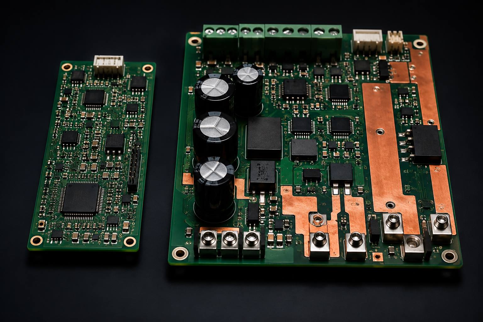
Case Study: Heavy Copper PCB Production for a Control and Drive Board
A customer shared Gerber files with EBest Circuit (Best Technology) for a Control and Drive PCB and asked our engineering team to review its manufacturability before quotation. The key technical point was clear: the Drive Board had a thick copper requirement, and the customer wanted confirmation that the board could be produced.
Project Background
- Product type: Control and Drive PCB
- Project stage: Gerber review and manufacturability confirmation
- Quantity: low-volume prototype stage
- Key requirement: thick copper on the drive board
- Customer concern: capability, clarification, and competitive production support
Customer Requirements
- Review Gerber details
- Confirm manufacturability
- Check drive board thick copper requirement
- Provide quotation after capability review
- Raise clarification questions if any production detail is unclear
EBest Circuit (Best Technology)’s Review Focus
For this type of project, the engineering review should not only check the board outline and layer count. The drive board’s thick copper requirement makes several areas more important:
- Copper weight requirement
- Copper spacing and etching feasibility
- Hole-to-copper clearance
- Copper balance across the board
- Large copper area manufacturability
- Solder mask coverage over heavy copper
- Plated hole reliability
- Surface finish requirement
- PCBA assembly compatibility, if assembly is required
- Test and inspection requirements
Project Value
This case shows why heavy copper drive boards should be reviewed before quotation. A drive board may carry more current than the control board, and its copper structure can affect production difficulty, cost, solderability, and reliability.
By reviewing manufacturability first, EBest Circuit (Best Technology) helps customers understand whether the board can be produced as specified, what details need clarification, and what process points may influence cost and delivery.
Typical Case Board Review Items
| Review Item | Focus |
|---|---|
| Board Type | Control and Drive PCB |
| Key Board | Drive board with thick copper requirement |
| File Review | Gerber and drill file review |
| Main Concern | Manufacturability confirmation |
| Copper Review | Copper weight, spacing, balance |
| Process Review | Etching, plating, solder mask, surface finish |
| Assembly Review | Connector and power component compatibility |
| Testing | Electrical test and inspection requirement |
This type of review is especially useful for customers preparing a prototype run before moving to larger production quantities.
What Files Are Needed for a Heavy Copper PCB Quote?
Customers do not need perfect documentation before contacting EBest Circuit (Best Technology). Available files can be sent first, and missing details can be clarified during engineering review.
For an initial heavy copper PCB quote, these files are helpful:
- Gerber files
- Drill files
- Board size
- Layer count
- Material requirement
- Board thickness
- Copper thickness
- Quantity
- PCB only or PCBA requirement
For a more accurate heavy copper PCB production review, please add if available:
- Stack-up
- Finished copper requirement
- Base copper requirement
- Surface finish
- Solder mask color
- Silkscreen color
- Controlled impedance requirement, if any
- High-current area notes
- Special spacing requirements
- Test requirements
- Report requirements
For PCBA quotation, please add:
- BOM
- Pick and place file
- Assembly drawing
- Component polarity notes
- Connector requirement
- Functional test requirement, if any
Cost is usually affected by:
- Copper weight
- Layer count
- Board size
- Material type
- Board thickness
- Hole structure
- Surface finish
- Solder mask process
- Assembly complexity
- Testing requirement
- Quantity
For a faster review, send your available Gerber files and project notes to sales@bestpcbs.com. EBest Circuit (Best Technology) will review the files and advise what additional details are needed before production.
FAQs About Heavy Copper PCB Production
What is heavy copper PCB production used for?
Heavy copper PCB production is used for boards that need higher current capacity, better thermal spreading, stronger power paths, and improved reliability in demanding applications.
When does a drive board need heavy copper?
A drive board may need heavy copper when it carries high current, controls motors, powers industrial systems, or includes power components such as MOSFETs, IGBTs, terminals, or high-current connectors.
What copper weight is considered heavy copper PCB?
Many projects start to be considered heavy copper when copper weight reaches 3 oz or above. Some customers also call 2 oz copper thick copper, especially for drive boards or power boards.
Can inner copper and outer copper be different?
Yes. A heavy copper PCB may use different copper weights on inner and outer layers. The requirement should be clearly stated in the production notes or stack-up.
What affects heavy copper PCB cost?
Cost is affected by copper weight, board size, layer count, material, board thickness, spacing, hole structure, surface finish, solder mask process, testing, assembly, and quantity.
Why is DFM review important for heavy copper PCB production?
DFM review helps confirm whether copper spacing, trace width, hole-to-copper clearance, solder mask coverage, copper balance, and board thickness are suitable for production.
Can heavy copper PCBs be assembled?
Yes. Heavy copper PCBs can be assembled, but the assembly process should consider thermal mass, solderability, connector type, power components, and reflow or soldering requirements.
What files are needed for a heavy copper PCB quote?
Gerber files, drill files, board size, layer count, material, board thickness, copper thickness, quantity, and PCB or PCBA requirement are helpful for the first review.
Does EBest Circuit (Best Technology) support heavy copper PCB production and assembly?
Yes. EBest Circuit (Best Technology) supports heavy copper PCB fabrication, DFM review, PCB layout manufacturability feedback, PCBA assembly, testing, and production documentation based on customer-provided files.
How can I start a heavy copper PCB quotation?
Send your available files and project notes to sales@bestpcbs.com. The engineering team will review manufacturability and advise whether additional information is needed before production.