PCB manufacturing PCB manufacturing
Home > Blog

heavy copper pcb price

Heavy Copper PCB for Battery Systems: BMS Design and DFM Guide
Monday, August 17th, 2026
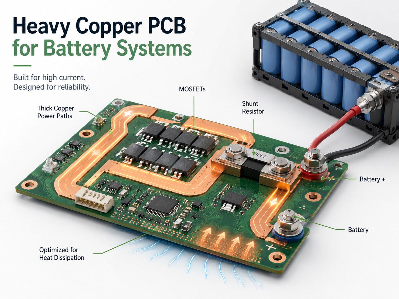
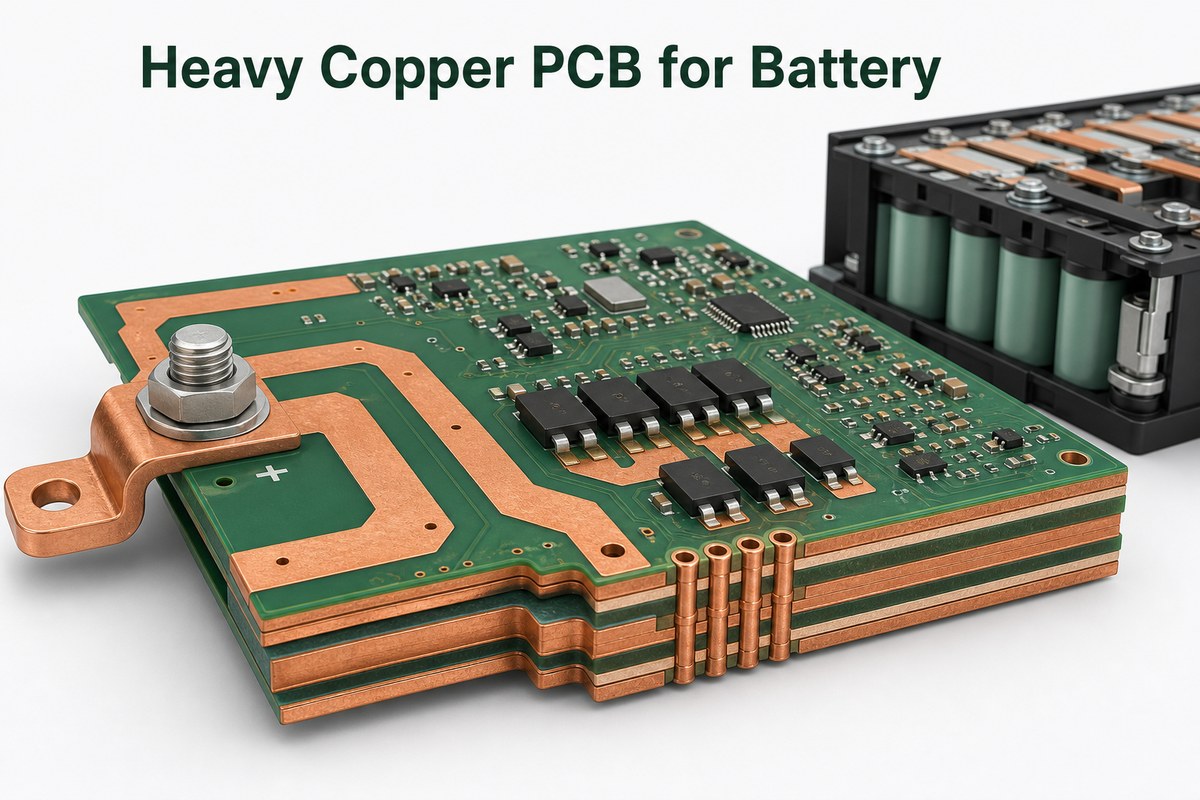
Heavy Copper PCB for Battery with thick copper power layers and a battery module

A heavy copper PCB for battery systems combines high-current power paths with the sensing, protection, and control circuits required by a battery management system (BMS). It can reduce conductor resistance and spread heat, but copper weight alone does not prove that a board can carry a target current. Trace geometry, layer position, vias, terminals, ambient temperature, duty cycle, airflow, and allowable temperature rise must be evaluated together.

This guide shows engineers and buyers how to turn current, voltage-drop, thermal, and mechanical requirements into a manufacturable PCB specification. It also explains where a busbar, embedded copper structure, or metal-core PCB may be a better fit.

What Is a Heavy Copper PCB for Battery Systems?

A heavy copper battery PCB uses thicker-than-standard copper on one or more layers to carry and distribute power between battery terminals, protection devices, switching components, loads, chargers, or contactors. The term has no single universal IPC threshold, so the fabrication drawing must state the finished copper requirement for every layer instead of relying on the words “heavy copper.”

In a BMS, the board may combine two very different electrical zones:

  • Power path: battery terminals, fuses, MOSFETs, shunts, pre-charge circuits, and high-current connectors.
  • Control path: cell-voltage measurement, temperature sensing, isolation, communications, and the BMS controller.

The layout should keep these functions electrically and thermally coordinated without forcing sensitive measurement traces to share noisy or high-resistance return paths.

Why Do Battery and BMS Designs Use Heavy Copper PCBs?

Battery and BMS designs use heavy copper when standard copper cannot meet the required resistance, temperature-rise, transient-current, or mechanical-connection targets within the available board area.

  • Lower resistance reduces I²R loss and voltage drop along the power path.
  • A larger copper cross-section spreads heat away from MOSFETs, shunts, fuses, and terminals.
  • Thicker copper can improve the mechanical robustness of high-current pads and bolted connections.
  • Power and control functions can remain on one assembly when the current level and manufacturing process allow it.

These benefits are conditional. A narrow neck-down, a small connector pad, insufficient via area, or an undersized terminal can become the actual bottleneck even when the main plane is thick.
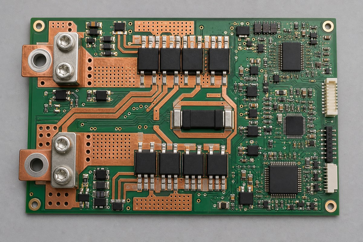
Battery BMS PCB showing wide heavy copper paths, MOSFETs, terminals, and via arrays

How Do You Reduce Voltage Drop in a Battery PCB?

Reduce voltage drop by lowering the resistance of the complete current path: increase copper cross-section, widen or shorten conductors, remove neck-downs, add properly sized parallel planes or via arrays, and reduce resistance at terminals, connectors, shunts, and solder joints. Increasing copper weight generally lowers DC resistance and conductor heating for the same width and length, but it does not create a universal ampacity rating because current capacity depends on the complete thermal environment.

IPC-2152 provides conductor-sizing guidance and charts for the relationship among current, conductor size, layer position, environment, and temperature rise. IPC now lists IPC-2152 as no longer maintained, so use it as an engineering reference and confirm the current customer, regulatory, and contract requirements for the project. IPC-2221C is the current generic printed-board design revision listed by IPC.

Input Why It Matters
Continuous and peak current Defines steady heating and short-duration stress.
Allowed voltage drop Sets the resistance budget for planes, neck-downs, vias, joints, and terminals.
Allowed temperature rise Determines how much conductor heating is acceptable above ambient.
Layer and cooling condition External and internal conductors reject heat differently.
Trace length and geometry Long paths, corners, slots, and narrow sections add resistance and hot spots.

For the DC path, calculate resistance across the full conductive loop, then confirm the result with electrothermal simulation or a representative test board. Include copper-temperature rise because copper resistance increases as it gets hotter.

What Copper Weight Should You Use for a Battery BMS PCB?

Choose copper weight from the continuous and peak current, trace geometry, allowable temperature rise, voltage-drop budget, layer position, cooling condition, and the fabricator’s process limits. There is no reliable universal copper weight for every BMS, so calculate the path first and confirm it through DFM and thermal testing.

Nominal 1 oz copper is approximately 35 µm (1.4 mil), while 2 oz copper is approximately 70 µm (2.8 mil). Thicker copper increases the total board thickness and can add lamination and drilling constraints.

Is 2 oz copper enough for a battery PCB? Two-ounce copper can be enough when the current path is sufficiently wide and short and the resulting voltage drop and temperature rise stay within the design limits. It is not automatically sufficient for a battery PCB; vias, terminals, connectors, ambient temperature, duty cycle, and cooling can change the result.

Copper Choice Typical Design Use Required Check
1 oz Signals, sensing, and lower-current distribution Confirm that width and temperature rise meet the load.
2 oz Moderate power paths where board area is available Verify neck-downs, vias, connector pads, and finished copper.
3 oz or heavier Higher-current or lower-resistance power sections Obtain an early stackup and DFM review for spacing, resin fill, drilling, and assembly.

Do not specify the same copper weight on every layer by habit. A mixed-copper construction may reduce cost and improve routing, but it requires a fabricator-approved stackup and clear finished-copper notes.

Heavy Copper PCB Stackup: What Must the Fabricator Review?

A heavy copper PCB stackup must balance finished copper, dielectric thickness, resin fill, symmetry, drill aspect ratios, total board thickness, and the electrical separation needed by the battery voltage.

  • State base foil and finished copper separately when plating changes the final value.
  • Keep the construction mechanically balanced to reduce bow and twist.
  • Provide enough resin to fill around thick etched copper without voids or thin dielectric areas.
  • Review via diameter, finished hole, annular ring, and plating for the real current and layer transitions.
  • Identify controlled-impedance or sensitive measurement layers that should not be distorted by adjacent heavy copper.
  • Define creepage and clearance from the maximum working voltage, pollution environment, coating, altitude, and applicable safety standard.

Do not select spacing from a generic voltage table alone. IPC-2221C is a generic design reference, while the end product may also be governed by battery, automotive, industrial, or safety requirements.
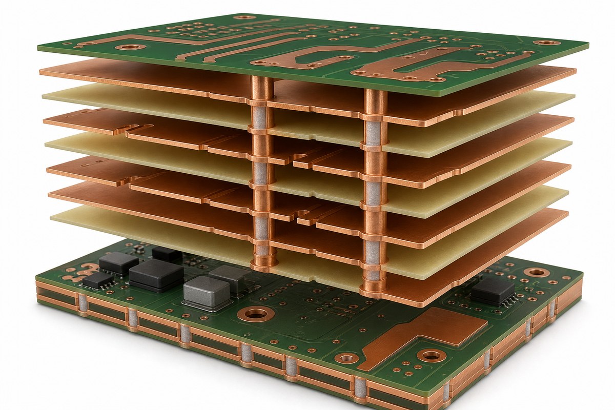
Exploded heavy copper PCB stackup with thick inner and outer copper layers and plated vias

How Should Thermal Management Be Verified?

Thermal management should be verified from the worst credible current, ambient temperature, enclosure, duty cycle, airflow, neighboring heat sources, and cooling path—not from copper weight alone.

  1. Build a loss model for copper paths, MOSFETs, shunts, fuses, connectors, and joints.
  2. Locate likely hot spots at neck-downs, via fields, terminal transitions, and component pads.
  3. Run coupled electrical and thermal simulation when current density or enclosure temperature is high.
  4. Measure a representative assembly under continuous current, peak-current pulses, charging, and fault-relevant conditions.
  5. Record copper or component temperature at thermal equilibrium and compare it with design limits and component derating.

Thermal vias help only when they connect to a useful heat-spreading or heat-sinking structure. A dense via field that terminates in a small internal island may add little cooling and can complicate fabrication.

Heavy Copper PCB Design: Which Rules Matter Most?

Heavy copper PCB design succeeds when every transition in the current path has enough electrical, thermal, and mechanical margin. The main plane is rarely the only feature that determines performance.

  • Avoid bottlenecks: keep effective width through pad entries, fuse areas, slots, and component breakouts.
  • Use gradual transitions: reduce abrupt width changes and sharp inside corners in high-current paths.
  • Size via arrays as conductors: calculate the total plated cross-section and current sharing, then verify fabrication limits.
  • Separate sensing from load current: use Kelvin connections for shunts and other low-level measurements.
  • Plan assembly: thick copper is a heat sink, so large terminals and components may need a tailored soldering profile or selective process.
  • Control copper balance: uneven density can affect etching, lamination, flatness, and soldering.

Use our PCB design tools for early trace and via checks, but treat calculator output as a starting point. The final design still needs stackup-specific DFM and thermal validation.

What Manufacturing Risks Should Be Cleared During DFM?

DFM should clear etching, plating, lamination, drilling, solder mask, surface finish, profiling, and assembly risks before the production data is released.

  • Minimum trace and spacing must match the copper thickness and process.
  • Finished copper tolerance must be reflected in resistance and clearance calculations.
  • Prepreg type and resin content must fill the topography around heavy copper.
  • Drill and plating requirements must support current-carrying vias and bolted terminals.
  • Solder mask dams and clearances must remain producible over tall copper features.
  • Panel design and copper distribution must control flatness and dimensional stability.
  • Assembly profiles must account for the board’s higher thermal mass.

Send the fabricator the native Gerber or ODB++ data, drill files, netlist, stackup, fabrication drawing, current requirements, and any impedance or safety notes early enough to change the layout.

Can a Heavy Copper PCB Replace a Busbar in a Battery Pack?

A heavy copper PCB can replace a busbar when its conductor geometry, terminals, thermal path, fault-current behavior, and mechanical strength meet the battery pack requirements. A busbar is usually preferable when very high current, low inductance, bolted connections, or limited board area makes the PCB solution impractical; many systems use both.

Structure Best Fit Main Tradeoff
Heavy copper PCB Integrated power, control, sensing, and interconnect on one board Thick-copper DFM and assembly thermal mass
Busbar or busbar PCB Very high current, low inductance, or robust bolted connections Mechanical integration and added part interfaces
Embedded copper PCB Localized high-current or heat-spreading sections Specialized construction and supplier capability
Metal-core PCB Heat spreading to a chassis or heatsink, often with simpler layer needs Electrical isolation and multilayer routing constraints

A hybrid assembly can be the best answer: a busbar handles the main battery current while a PCB carries gate drive, sensing, balancing, and communication circuits.

How Should Heavy Copper Battery PCBs Be Tested?

Testing should prove conductor integrity, isolation, resistance, thermal behavior, and assembly quality under the conditions defined by the battery system.

  • Fabrication checks: electrical test, finished copper verification, hole and plating inspection, and microsection review.
  • Low-resistance measurement: four-wire measurement across the complete current path, including terminals and joints.
  • Thermal test: continuous and pulsed load testing with temperature measurements at predicted hot spots.
  • Isolation test: apply the project-specific dielectric or insulation test method where required.
  • Assembly inspection: verify solder joints, voiding criteria where relevant, terminal torque process, and cleanliness.
  • Functional test: confirm sensing accuracy, MOSFET switching, protection thresholds, communications, and fault behavior.

The acceptance criteria should be agreed before fabrication. “Passes current” is not enough unless the allowable voltage drop, temperature rise, duration, ambient, and measurement points are defined.

Quality engineer inspecting a heavy copper battery PCB with microscopy and thermal test equipment

What Determines Heavy Copper PCB Price?

Heavy copper PCB price is driven by copper weight, layer count, board and panel size, stackup complexity, spacing, drilling, plating, surface finish, testing, quantity, and yield risk. The same outline can have very different pricing when the copper distribution or DFM margin changes.

The fastest way to obtain a useful quotation is to provide fabrication data rather than a layer count and copper weight alone. Pricing may increase when a design requires unusual material combinations, tight spacing at high copper weight, extensive resin filling, special via structures, strict flatness, impedance control, heavy selective plating, or additional coupons and tests.

What Files Should You Send for a Heavy Copper Battery PCB Quote?

  • Gerber or ODB++ files, NC drill files, IPC-356 netlist, and fabrication drawing
  • Layer count, board thickness, material requirements, and proposed stackup
  • Base and finished copper for each layer
  • Continuous current, peak current, pulse duration, and duty cycle
  • Maximum allowed voltage drop and temperature rise
  • Maximum working voltage and applicable insulation or safety standard
  • Terminal, connector, fastener, and assembly requirements
  • Surface finish, solder mask, controlled impedance, and test requirements
  • Prototype quantity, production volume, and target schedule

At EBest Circuit, we manufacture heavy copper PCBs. Review our heavy copper PCB manufacturing page, then send us the complete data package for a stackup and DFM review.

FAQ About Heavy Copper PCB for Battery Systems

Do batteries have PCBs?

Many battery packs use one or more PCBs for monitoring, protection, balancing, communications, and switching. Small packs may use a compact protection board, while larger systems may use a separate BMS controller and high-current switching assembly.

How thick is 2 oz of copper on a PCB?

Nominal 2 oz copper is about 70 µm or 2.8 mil before process tolerances and final plating effects are considered.

How thick is 3 oz of copper on a PCB?

Three-ounce copper is commonly treated as roughly three times the nominal thickness of 1 oz foil, but the released drawing should use the fabricator’s approved finished-copper specification and tolerance rather than a nominal conversion alone.

How much voltage can a PCB handle?

A PCB has no single voltage limit. The safe working voltage depends on conductor spacing, creepage, clearance, dielectric construction, coating, contamination, altitude, manufacturing tolerances, and the applicable product-safety standard. Define the maximum working and transient voltage before the stackup and spacing review.

How does copper weight affect voltage drop in a battery PCB?

Heavier copper increases conductor cross-sectional area and generally reduces resistance and voltage drop when width and length stay the same. The total drop still includes neck-downs, vias, shunts, connectors, terminals, solder joints, and the higher resistance of hot copper.

What information affects heavy copper PCB price for a battery project?

Price is affected by copper weight, layer count, board and panel size, stackup, material, spacing, drilling, plating, surface finish, test requirements, quantity, and expected yield. Complete fabrication data produces a more useful quotation than copper weight and dimensions alone.

When is a busbar better than a heavy copper PCB?

A busbar is often better when current, mechanical connection, low inductance, or board-area constraints make a PCB power path impractical. A hybrid busbar-plus-control-PCB design is common in high-power systems.

Technical references: IPC-2152 table of contents and the IPC standards revision table.

How Can EBest Circuit Support Your Heavy Copper Battery PCB Project?

At EBest Circuit, we manufacture FR4 heavy copper PCBs with standard-process copper thickness up to 5 oz on inner and outer layers. Copper above 5 oz and up to 20 oz is handled as a special process, while the extreme heavy copper capability listed up to 200 oz requires project-specific engineering evaluation. We also provide DFM support for stackups, finished copper, high-current transitions, via arrays, terminals, and assembly requirements.

If your battery or BMS design must control voltage drop, temperature rise, current-path bottlenecks, or manufacturing risk, we can review the construction and help identify practical changes before fabrication. This is especially useful when the design combines thick copper, sensitive BMS measurement, bolted terminals, or strict thermal limits.

Send your Gerber or ODB++ data, drill files, stackup, continuous and peak current, voltage-drop target, temperature-rise limit, maximum working voltage, quantity, and assembly needs to sales@bestpcbs.com. We will review the project requirements and prepare a heavy copper PCB quotation.
You may also like

Heavy Copper PCB for Battery Systems: High-Current Design Guide
Monday, August 17th, 2026

Battery boards have an unusual job. One part of the PCB may be measuring tiny cell-voltage changes, while another part carries high current through MOSFETs, shunts, terminals, and power copper. That is where a heavy copper PCB for battery systems becomes useful.

Thicker copper can lower conductor resistance, reduce voltage drop, and spread heat more effectively. But copper weight alone does not make a good high-current board. Trace geometry, vias, connectors, thermal paths, and the actual battery current route matter just as much.

So instead of asking, “How many amps can 4 oz copper carry?”, start with:

  • What is the continuous current?
  • What is the peak current?
  • How long does the peak last?
  • What voltage drop is acceptable?
  • How much temperature rise is allowed?
  • Does the full battery current actually pass through the PCB?

Those answers determine whether you need 2 oz, 4 oz, heavier copper, or perhaps a different power-distribution structure entirely.

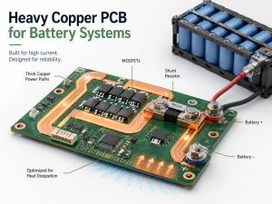
Heavy copper PCB for battery systems with thick copper power paths, MOSFETs, shunt resistor, and battery terminals

What Is a Heavy Copper PCB for Battery Applications?

A heavy copper PCB uses thicker-than-standard copper conductors to support higher current, lower resistance, and improved heat spreading.

In battery electronics, it is commonly found in:

  • Battery management systems
  • EV battery modules
  • Energy storage systems
  • Battery chargers
  • High-current protection boards
  • Power distribution modules
  • Industrial battery packs

The important distinction is between the control section and the power section.

The control section may contain:

  • MCU
  • Cell monitoring ICs
  • Communication circuits
  • Temperature sensing
  • Gate drivers

The power section may contain:

  • Battery terminals
  • MOSFETs
  • Fuses
  • Relays
  • Current shunts
  • Output connectors

Heavy copper is usually most valuable in the second group. Using thick copper everywhere often adds manufacturing cost without adding much electrical benefit.

Does Every Battery or BMS PCB Need Heavy Copper?

No. A board does not need heavy copper simply because it is used in a battery system.

A sensing-only BMS may work well with standard copper. A protection board carrying the full pack current through MOSFETs and PCB conductors has a very different requirement.

Before specifying heavy copper, check:

  • Continuous current
  • Peak current and duration
  • Available conductor width
  • Current-path length
  • Allowable temperature rise
  • Voltage-drop limit
  • Cooling conditions
  • Number of current-carrying layers
  • Connector and terminal structure

The circuit architecture matters too. Two systems may both be rated at 100 A:

  • Design A: The PCB handles monitoring and switching control while a busbar carries most of the current.
  • Design B: The full 100 A passes through the PCB, MOSFETs, shunt, and output terminal.

Design B has a much stronger case for heavy copper. A better starting question is: Where does the battery current actually flow?

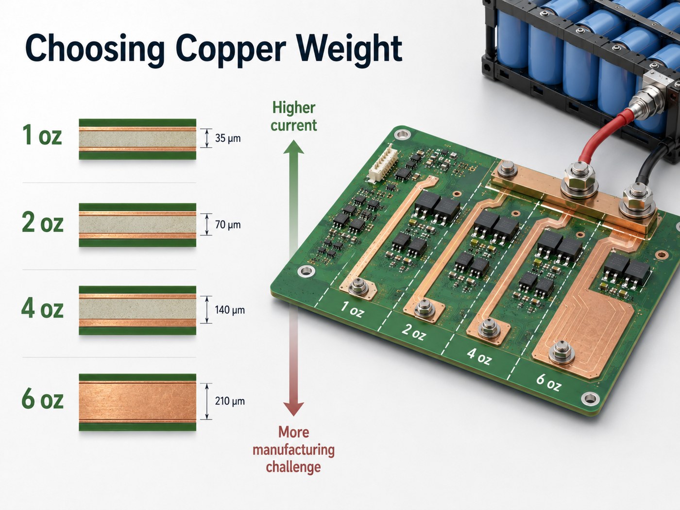
How Much Copper Weight Does a Battery PCB Need?

There is no single correct copper weight for battery PCBs.

Copper Weight Approx. Copper Thickness Typical Role
1 oz 35 µm Signals and light power
2 oz 70 µm Moderate power circuits
3 oz 105 µm Higher-current sections
4 oz 140 µm Heavy-current power paths
6 oz 210 µm Industrial high-current boards
10 oz 350 µm Very heavy power distribution

This is a thickness comparison, not a current-rating table. A 20 mm-wide 4 oz copper plane has far more conductor area than a 3 mm-wide trace made from the same copper weight.

Copper selection should consider:

  • Current
  • Trace width
  • Trace length
  • Layer location
  • Number of parallel layers
  • Temperature-rise target
  • Available board area

More copper is not automatically better. Very thick copper can affect minimum trace and spacing, etching accuracy, lamination, solder-mask coverage, board thickness, and cost.

Comparison of 1 oz, 2 oz, 4 oz, and 6 oz copper weight for battery PCB design

How Much Current Can a Heavy Copper PCB for Battery Carry?

Copper weight by itself cannot answer this question.

R = ρL / A

Where:

  • R = resistance
  • ρ = copper resistivity
  • L = conductor length
  • A = cross-sectional area

For a PCB conductor:

A = W × T

Where W is trace width and T is copper thickness.

Consider a simplified example:

  • Length: 100 mm
  • Width: 20 mm
  • Copper: 4 oz, about 0.14 mm thick

Cross-sectional area:

20 × 0.14 = 2.8 mm²

The ideal room-temperature resistance is roughly 0.62 mΩ.

At 50 A:

Vdrop ≈ 50 × 0.00062 = 31 mV

P ≈ 50² × 0.00062 = 1.55 W

At 100 A, resistive heating becomes roughly four times higher because:

P = I²R

This is only a first-pass electrical calculation. Actual conductor temperature also depends on:

  • Internal or external layer
  • Nearby copper
  • PCB thickness
  • Airflow
  • Ambient temperature
  • MOSFET heat
  • Connector losses
  • Duty cycle

For serious high current PCB design, conductor sizing should be evaluated using IPC-2152 principles rather than a simple “amps per oz” shortcut.

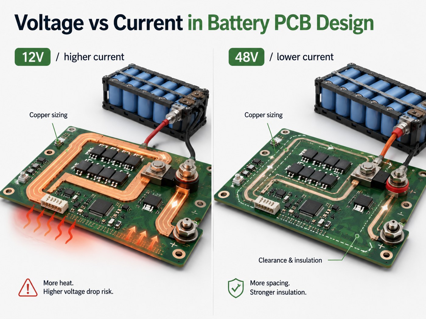
How Does Battery Voltage Affect Heavy Copper PCB Design?

Higher battery voltage does not automatically require thicker copper.

Current mainly influences:

  • Copper thickness
  • Trace width
  • Conductor resistance
  • Voltage drop
  • Heat generation

Voltage mainly influences:

  • Creepage
  • Clearance
  • Insulation
  • Component ratings
  • Connector ratings
  • Protection requirements

For approximately 1,200 W:

  • 12 V system: about 100 A
  • 48 V system: about 25 A

The 48 V system has the higher voltage, but the 12 V system carries much more current and may need a heavier conductor.

Useful rule: Current determines how much conductor you need. Voltage determines how much electrical separation you need.
Battery PCB design comparison showing higher current at 12V and greater spacing and insulation emphasis at 48V

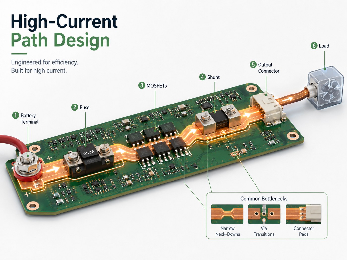
How Should You Design High-Current PCB Paths for Battery Systems?

Treat the high-current section as one complete path:

Battery Terminal → Fuse → MOSFET → Shunt → Output Connector → Load

Every narrow section along that route matters.

Useful layout practices include:

  • Keep high-current paths short.
  • Use broad copper pours instead of long narrow traces.
  • Avoid abrupt neck-downs near pads and terminals.
  • Use multiple copper layers when current sharing is practical.
  • Minimize unnecessary layer transitions.
  • Design the return path with the same care as the forward path.
  • Keep high-current switching areas compact.

Pay particular attention around MOSFET drain/source pads, shunt resistors, fuses, connectors, screw terminals, and via transitions.

A 30 mm-wide plane does not help much if the current must squeeze through a 3 mm-wide copper neck before reaching the connector.

High-current battery PCB current path from battery terminal through fuse, MOSFETs, shunt, output connector, and load

How Should Vias, Connectors, MOSFETs and Current-Sense Paths Be Designed?

The PCB trace is only one part of the resistance chain.

Power vias

When current changes layers, use an appropriate via array rather than relying on one or two vias.

  • Via count
  • Finished hole size
  • Barrel copper
  • Via placement
  • Current distribution

Connectors and terminals

Check more than the connector’s headline current rating.

  • Contact resistance
  • Pad area
  • Solder-joint area
  • Copper entry width
  • Mechanical load
  • Terminal heating

MOSFET areas

Provide generous copper around high-current source and drain paths. For parallel MOSFETs, try to keep the electrical path balanced so that one device does not carry disproportionately more current.

Current sensing

For shunt measurements, use proper Kelvin sensing where required. Keep the low-level sense traces separate from the main high-current path so voltage drop in the power copper does not distort the measurement.

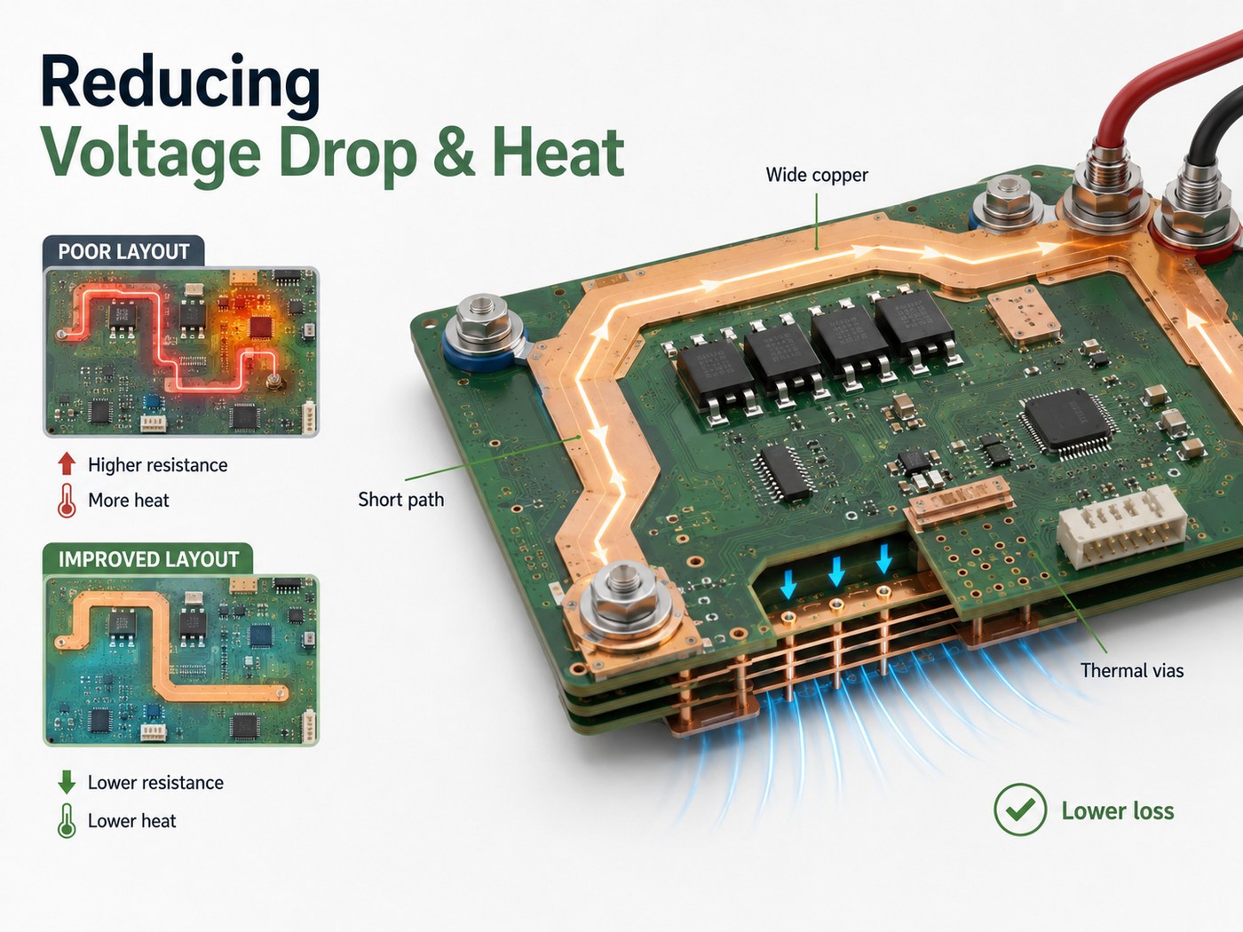
How Can You Reduce Voltage Drop and Heat in a Battery PCB?

Voltage drop and conductor heating both come from resistance.

Vdrop = I × R

Ploss = I² × R

At 100 A, even 1 mΩ produces:

  • 0.1 V voltage drop
  • 10 W of heat

Ways to reduce resistance include:

  • Increase conductor width
  • Increase copper thickness
  • Shorten the power path
  • Use parallel copper layers
  • Improve via transitions
  • Remove neck-down areas
  • Use low-resistance terminals
  • Increase contact and solder area

For thermal management, also consider:

  • Large copper spreading areas
  • Thermal vias
  • Connected internal planes
  • Heatsinks
  • Thermal interface materials
  • Enclosure conduction
  • Airflow

Voltage drop and temperature rise should be checked together. They are two symptoms of the same resistance problem.

Battery PCB layout comparison showing how wide copper, short current paths, and thermal vias reduce voltage drop and heat

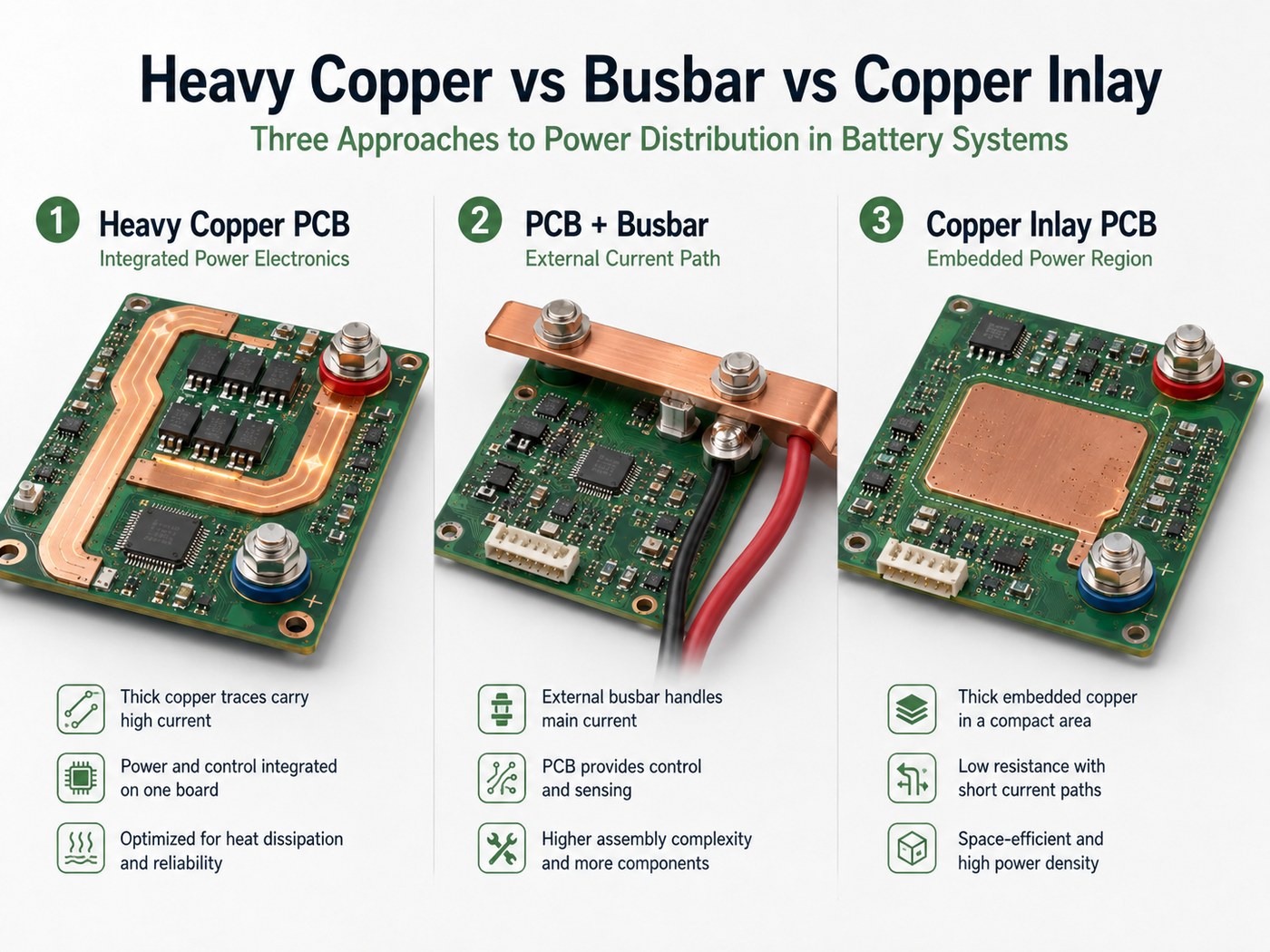
Heavy Copper PCB vs Busbar vs Copper Inlay: Which Is Better for Battery Systems?

Heavy copper is not always the final answer. As current increases, alternative structures may become more practical.

Solution Current Potential PCB Integration Space Efficiency Typical Use
Heavy Copper PCB High Excellent Good BMS, chargers, power control
PCB + Busbar Very high Moderate Moderate Battery packs, power distribution
Copper Inlay PCB Very high locally Excellent Very good Compact high-power modules

Heavy copper PCB

Best suited when the board needs to combine power distribution, MOSFETs, shunts, protection, connectors, and control electronics.

PCB with busbar

A busbar is attractive when very low resistance and very high current capacity take priority over having all current carried through the PCB.

Copper inlay PCB

Copper inlay concentrates thick copper in specific high-current or high-heat regions. It is useful when board space is limited or local current density is very high.

The selection should be based on the complete electrical, thermal, mechanical, and manufacturing picture—not current alone.

Comparison of heavy copper PCB, PCB plus busbar, and copper inlay PCB for battery systems

What DFM Challenges Matter in Heavy Copper Battery PCB Design?

Heavy copper changes the fabrication process, so DFM should start before the layout is frozen.

A practical heavy copper PCB stackup must balance finished copper, dielectric thickness, resin fill, symmetry, and achievable spacing.

  • Etching: Thick copper makes fine traces and tight spacing harder to control.
  • Spacing: Rules suitable for 1 oz copper may not suit 4 oz or 6 oz copper.
  • Copper-to-hole clearance: Heavy copper around drilled features needs adequate manufacturing margin.
  • Lamination: Deep spaces between thick copper features must fill reliably with resin.
  • Copper balance: Large asymmetric copper areas can increase warpage risk.
  • Solder mask: Thick copper creates more surface topography.
  • Board thickness: Multiple heavy-copper layers can significantly increase the finished thickness.

Before release, review this checklist:

  • Finished copper weight confirmed for every layer
  • Trace width and spacing checked
  • Copper-to-hole clearance verified
  • High-current vias reviewed
  • Copper distribution balanced
  • Stackup and resin requirements confirmed
  • Solder-mask capability checked
  • Final board thickness verified
  • Terminal and connector footprints reviewed
  • Narrow current bottlenecks identified
  • Creepage and clearance checked

A layout can be electrically sound and still be expensive or difficult to build. Early DFM catches that before tooling.

How Much Does a Heavy Copper PCB for Battery Applications Cost?

There is no meaningful universal price for a heavy copper battery PCB.

A heavy copper PCB price therefore depends on the complete fabrication specification, not copper weight alone.

Cost depends on the complete build, including:

  • Copper weight
  • Number of heavy-copper layers
  • PCB dimensions
  • Layer count
  • Board thickness
  • Trace and spacing requirements
  • Via structure
  • Surface finish
  • Material
  • Quantity
  • Testing requirements
  • Mixed copper constructions

A spacious 4-layer board with 4 oz copper may be easier to manufacture than a compact multilayer board with the same copper weight but tight spacing.

For purchasing teams, a better question than “How much is a 4 oz PCB?” is: What stackup meets our current and thermal targets with the lowest practical manufacturing complexity?

What Information Should You Provide for a Heavy Copper Battery PCB Quote?

A good RFQ should describe both the PCB and the electrical requirement.

Experienced heavy copper PCB manufacturers also need the current profile and thermal limits so they can review the design against the proposed construction.

  • Gerber or ODB++ files
  • Fabrication drawing
  • Stackup
  • Finished copper weight by layer
  • Material
  • Board thickness
  • Surface finish
  • Nominal battery voltage
  • Maximum voltage
  • Continuous current
  • Peak current
  • Peak-current duration
  • Duty cycle
  • Allowable temperature rise
  • Maximum voltage drop
  • Operating temperature
  • Connector or terminal requirements
  • IPC acceptance class
  • Quantity
  • Reliability or test requirements

For high-current boards, mark the main current route where possible:

BAT+ → Fuse → MOSFET Bank → Shunt → PACK+

Avoid sending only 48 V / 100 A. That does not tell the PCB manufacturer whether 100 A is continuous or momentary, how wide the conductor is, or how the current transitions between layers.

FAQs About Heavy Copper PCB for Battery Systems

What copper thickness is best for a high-current battery PCB?

There is no universal best value. Copper thickness should be selected together with trace width, current, conductor length, temperature-rise limit, and voltage-drop target.

Is 2 oz copper enough for a battery BMS PCB?

Sometimes. A monitoring-focused BMS may not need heavy copper at all. If the full battery current flows through the PCB, conductor geometry and thermal conditions should be checked before choosing 2 oz.

How much current can a 3 oz copper PCB carry?

There is no fixed current rating. A wide 3 oz plane can carry much more current than a narrow 3 oz trace. Layer position, temperature rise, and thermal environment also matter.

How much current can a 4 oz copper PCB carry?

Again, 4 oz describes copper thickness, not amperage. Trace width, length, layer structure, vias, and cooling conditions determine the practical current limit.

Does higher battery voltage require thicker PCB copper?

Not necessarily. Current primarily drives conductor sizing. Voltage mainly affects creepage, clearance, insulation, and component ratings.

When should I use a heavy copper PCB instead of a busbar?

Heavy copper works well when high-current distribution needs to remain integrated with MOSFETs, shunts, connectors, and control circuitry. At very high current, a busbar or hybrid PCB-busbar design may be more practical.

Can heavy copper PCB reduce voltage drop?

Yes. A larger conductor cross-section reduces resistance, which helps lower voltage drop. Trace length, connectors, vias, and local bottlenecks still need to be considered.

Does heavy copper PCB improve heat dissipation?

It can reduce resistive losses and spread heat over a larger copper area. Final temperature still depends on components, airflow, enclosure design, and the overall thermal path.

What is the difference between a heavy copper PCB and a high-current PCB?

Heavy copper PCB describes the board construction. High-current PCB describes the design purpose. A high-current board may use heavy copper, busbars, copper inlays, or a combination of these.

What information does a PCB manufacturer need to quote a heavy copper battery board?

Provide the fabrication files, stackup, copper weight, board thickness, material, quantity, and surface finish. For engineering review, also include battery voltage, continuous current, peak current, peak duration, temperature-rise limit, and voltage-drop requirement.

How Can EBest Circuit Support Your Heavy Copper Battery PCB Project?

Send us your Gerber or ODB++ files, fabrication drawing, target copper weight, stackup, quantity, and current and thermal requirements. Our team can review the build for manufacturability and prepare a project-specific quotation.

You may also like