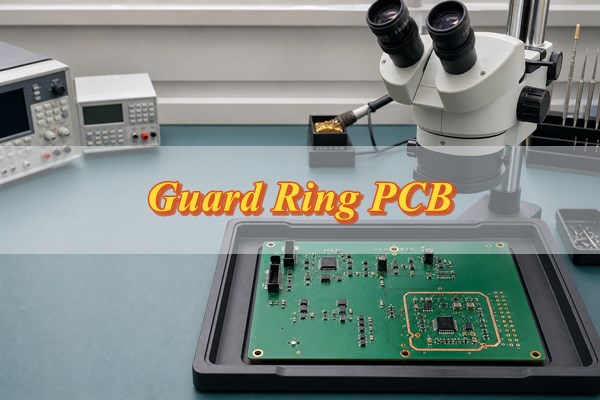
A guard ring pcb uses a conductive trace around a high-impedance node to intercept surface leakage before it reaches the sensitive copper. The guard is most effective when a low-impedance source drives it close to the protected node’s voltage. It is not automatically a grounded shield, a board-edge ground ring, a via fence, or the annular copper around a drilled hole.
A successful layout starts with the circuit, not the shape. Identify the node whose allowable error is comparable to expected leakage, select a guard voltage that minimizes the voltage across unwanted surface paths, enclose the complete sensitive path, control contamination, and test the assembled prototype under realistic conditions.
What Is a Guard Ring PCB?
A PCB guard ring is copper placed around a leakage-sensitive node and connected to a controlled low-impedance potential. Its job is to collect current that would otherwise cross the board surface into the protected input. The protected object may be an op-amp input pin, a photodiode node, a transimpedance feedback junction, an electrometer input, or another point where picoampere-level current can create a material error.
The word “ring” describes electrical enclosure, not necessarily a perfect circle. The copper may form an irregular closed trace around pads, a short route, and selected component terminals. Components that connect the sensitive node to lower-impedance circuitry often straddle the guard so the guarded copper does not extend beyond the enclosure.
Three similar-looking structures solve different problems. A driven guard reduces leakage into a high-impedance node. A grounded board-edge ring can support electromagnetic containment, while a PCB ground loop is an unwanted return-current path. An annular ring is the copper surrounding a drilled hole. Treating these features as interchangeable can create a layout that looks protected but does not control the intended current path.
How Does a Guard Ring Work on a PCB Layout?
A guard ring works by reducing the voltage that drives leakage toward the sensitive node and by providing that leakage with a lower-impedance destination. Surface current is governed by the voltage across an unintended resistance. For a simplified path, Ileak = (Vsource – Vnode) / Rsurface. This relationship is useful for estimating scale, not for assigning one fixed resistance to every board.
Suppose a nearby conductor is 5 V away from a sensitive input and the contaminated surface path is 100 Gohm. The simplified leakage is 50 pA. If a low-impedance guard reduces the voltage across the final path to 1 mV, the same assumed resistance would correspond to 10 fA. Real layouts contain several parallel surface and bulk paths, so this calculation is a design check rather than a guaranteed result.
The guard must remain low impedance across the relevant frequency range. A weak source can move when it collects leakage or coupled current. A long guard can also add capacitance to the sensitive network or load its driver. The circuit therefore needs both a suitable DC potential and adequate driver stability.
When Should You Use a Guard Ring in PCB Design?
Use a guard ring when board leakage can consume a meaningful part of the circuit’s error budget. The decision depends on source impedance, allowable input current, adjacent voltages, contamination exposure, humidity, temperature, and the input behavior of the selected device. A guard is common in low-current measurements, but it is not a universal upgrade for every analog trace.
- Photodiode and transimpedance inputs: leakage entering the summing node can appear as false sensor current and create output offset.
- Electrochemical and pH interfaces: high source impedance makes the input vulnerable to small surface currents and residue.
- Precision op-amp inputs: a guard may be justified when PCB leakage is comparable to input bias current or the permitted offset-current error.
- Multiplexer channels: off-channel voltage and package or board leakage may disturb a high-impedance selected channel.
- Low-resistance signal paths: a driven guard is usually unnecessary when ordinary spacing, a continuous reference plane, and clean routing already keep leakage far below the error budget.
Do not use a driven guard as a substitute for fixing a broken return path, inadequate creepage, poor shielding, excessive sensitive-trace length, or an unsuitable component. High voltage safety spacing and RF isolation require their own analysis.
Should a PCB Guard Ring Connect to Ground or a Driven Voltage?
Connect the guard to the lowest-impedance node that closely follows the protected node’s operating voltage; use ground only when ground satisfies that condition. A grounded guard around a node that sits several volts above ground can increase the electric field across the remaining insulation and may create more leakage than a properly driven guard.
| Circuit condition | Guard connection to evaluate | Main check |
| Protected node remains near ground | Quiet, low-impedance ground | Confirm ground noise and return current do not modulate the guard |
| Noninverting high-impedance input | Low-impedance node that tracks the input, often selected from the amplifier topology | Verify common-mode range, stability, and voltage tracking |
| Inverting or transimpedance summing node | A low-impedance reference near the virtual-node potential | Confirm the guard does not enclose or load the wrong net |
| Dedicated guard-output device | Manufacturer-defined guard output | Follow its routing, load-capacitance, and stability guidance |
Choose the connection from the device data sheet and circuit configuration rather than copying a nearby layout. The correct net can change between inverting, noninverting, buffer, multiplexer, and electrometer circuits. Check the guard over the full input range, during power sequencing, and when the driver saturates or loses power.
How Should You Design a Guard Ring on a PCB Layout?
Design the guard to enclose every practical surface path into the sensitive node while keeping the protected copper short. Start at the package pin, follow the complete high-impedance net, and identify every pad, via, connector, test point, and component lead that can create a bypass around the guard.
- Define the protected net: mark the exact package pins, pads, vias, feedback junctions, connector contacts, and test features whose leakage allowance is limited. Extend the boundary only as far as the high-impedance condition exists. If a series component changes the node to a low-impedance signal, place that component at the boundary instead of guarding unnecessary downstream copper.
- Select the guard source: document the expected guard voltage, output impedance, operating range, startup state, and capacitive-load limit. Check the voltage difference between the guard and protected node at the minimum and maximum signal levels, not only at the nominal bias point. Also review power-up, shutdown, saturation, and disconnected-sensor conditions because the two nodes may temporarily separate.
- Shorten sensitive copper: place the input device and critical passive components before drawing the guard. Keep the guarded trace direct, minimize exposed pad area, and avoid optional test pads or long connector stubs inside the enclosure. The ring should protect a compact node; it should not be used to justify a longer high-impedance route.
- Enclose the surface path: route a continuous guard between the sensitive copper and nearby conductors that can drive leakage. Close practical gaps around pads and component bodies, but do not cut through required land patterns or assembly clearances. Resistors, capacitors, or other boundary components can straddle the guard when one terminal belongs to the protected node and the other belongs outside it.
- Review every layer: inspect the same XY area on the top, bottom, and internal layers. A top-layer ring cannot intercept contamination on the bottom surface, and an unrelated plane directly below can add capacitance or create a field across the laminate. For a through-hole input or a bottom-side sensitive path, evaluate guarding on both outer layers and keep unrelated copper away from the protected volume.
- Add guarded transitions deliberately: connect top and bottom guard copper with guard-net vias when both surfaces need the same controlled potential. Place enough connections to avoid isolated copper and excessive guard impedance, but do not copy RF via-fence spacing rules into a low-leakage circuit without an electrical reason. Keep ordinary ground, power, and signal vias outside the guarded boundary unless the schematic explicitly requires them there.
- Apply fabrication constraints: choose guard width, clearance, annular geometry, solder-mask treatment, and copper-to-pad spacing that the selected PCB process can reproduce and inspect. Put the guard net name, mask openings, controlled keepouts, and any unusual cleaning requirement into the fabrication and assembly data. Confirm that automated optical inspection, probing, rework access, and depanelization will not damage or contaminate the guarded area.
- Check parasitic effects: estimate guard-to-node capacitance, driver loading, settling time, and stability instead of assuming more copper is always better. A wide guard or large guard plane may improve interception yet increase capacitive load on the driver and coupling to the sensitive node. Review the amplifier or guard-driver guidance, then verify settling and oscillation behavior on the assembled prototype.
There is no universal guard width or clearance. The fabricator’s minimum feature rules establish what can be built, but they do not prove the electrical design. Voltage difference, contamination exposure, assembly residues, device guidance, guard-driver capability, and measured leakage determine whether the guard ring pcb geometry is adequate.
Before releasing Gerbers, perform a boundary walk from the sensitive pin around the complete enclosure. Confirm that no pad, via, plane edge, mask-defined opening, test point, or connector contact creates an unguarded shortcut. This final spatial review is especially important when schematic nets appear correct but library courtyards, plane pours, or bottom-side features have changed during layout.
How Should You Handle Solder Mask, Cleaning, and Conformal Coating Around a Guard Ring?
Treat solder mask, cleanliness, and coating as electrical design variables because each one can change the leakage path around the guarded node. The production drawing and assembly process should define the required surface condition instead of leaving it to general workmanship.

- Choose the solder-mask strategy: decide separately whether the guard copper and protected node remain covered or exposed. An exposed guard can collect surface current directly, but exposed copper requires a compatible final finish and stricter handling. Solder mask may protect copper mechanically, yet its surface and interfaces are still possible leakage paths.
- Define mask openings precisely: place openings and clearances in the fabrication data rather than relying only on a general note. Check registration tolerance so mask does not partly cover a narrow guard, expose unintended sensitive copper, or create small residue-trapping edges around pads.
- Control flux and cleaning residue: specify the flux system, cleaning chemistry, rinse quality, drying method, and acceptance criteria needed for the leakage target. Flux residues, fingerprints, cleaning-agent residue, dust, and absorbed moisture can reduce surface resistance even when the board looks visually clean.
- Protect the surface after cleaning: use clean gloves, covered storage, controlled fixtures, and suitable packaging between cleaning, inspection, testing, and coating. Avoid touching the guarded area with probes or handling tools that can transfer oils or particles back onto the surface.
- Apply conformal coating only to a clean assembly: coating can reduce exposure to moisture and contamination, but it cannot reliably seal in residue and repair an uncontrolled process. Voids, poor adhesion, incomplete cure, trapped moisture, and coating beneath connectors or sockets can create leakage paths that are difficult to inspect.
- Qualify the completed surface system: compare leakage before and after assembly cleaning, then repeat the measurement after coating when coating is required. Use the intended humidity, temperature, bias voltage, settling time, and fixture arrangement so the test represents the conditions that drive the real error budget.
What Common PCB Guard Ring Design Mistakes Should You Avoid?
The most damaging mistakes are electrical, not geometric: the wrong guard voltage, an incomplete enclosure, or an untested contamination path. A visually continuous ring can still fail if the sensitive net escapes through a via, a component pad, the opposite surface, a connector, or a test fixture.
- Grounding by habit: ground is not the correct guard potential when it is far from the sensitive-node voltage.
- Guarding the wrong node: surrounding an amplifier output or low-impedance route does not protect the actual high-impedance input.
- Leaving a bypass path: copper, pads, vias, sockets, and fixtures outside the enclosure can carry leakage around the ring.
- Ignoring the opposite surface: through-hole pins and bottom-side contamination can bypass a top-only guard.
- Overloading the driver: excessive guard area or long routing can increase capacitance and destabilize a buffer or slow settling.
- Assuming solder mask is an insulator: mask condition, residue, moisture, and voltage determine the actual surface path.
- Skipping process documentation: an unmarked mask opening or ambiguous guard net can be changed during fabrication, assembly, or revision.
- Testing only in a clean room state: a dry bench result may not represent the humidity and contamination conditions of the application.
How Do You Review and Test a Guard Ring PCB?
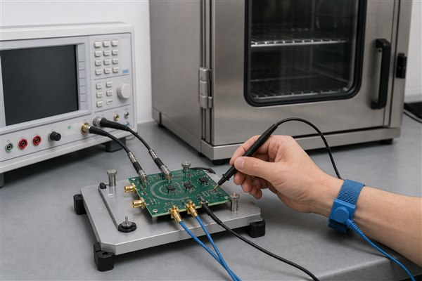
Review the design before release, then measure the assembled prototype under the voltage and environmental states that create the worst credible leakage. DRC can confirm spacing and connectivity, but it cannot prove that the chosen guard voltage is correct or that the finished assembly meets the error budget.
- Audit the schematic: identify the exact protected node, nearby aggressor voltages, intended guard source, signal range, and allowable leakage contribution to the total error budget. Review normal operation as well as power-up, shutdown, overload, open-sensor, and saturation states so the guard does not become the aggressor during an abnormal condition.
- Trace the physical boundary: follow the protected copper on every layer and inspect pads, vias, test points, connectors, package bodies, and plane edges around it. Use Gerber or ODB++ data in addition to the PCB editor view because copper pours, mask openings, and manufacturing outputs can differ from the simplified design display.
- Verify guard connectivity: confirm that all intended guard segments and guard vias connect to the correct net and that no isolated copper island remains. Check clearance to the protected node and unrelated nets with DRC, then visually review areas where component pads or narrow routing create gaps that an automated rule may accept.
- Measure guard tracking: measure both the protected-node voltage and the guard voltage, then calculate their difference across the full operating range. Repeat the measurement during startup, shutdown, overload, and recovery; a small steady-state difference does not prove that the guard tracks correctly during transitions.
- Establish a controlled baseline: measure input-referred offset or leakage with a known source condition and a fixture whose insulation, cables, connectors, and instruments contribute less error than the limit being evaluated. Record warm-up and settling time, and use shielding where necessary so noise or fixture leakage is not mistaken for PCB leakage.
- Compare production states: repeat the same measurement on the assembled board before cleaning, after the qualified cleaning process, and after conformal coating when coating is specified. Keep the circuit bias, fixture, stabilization time, and environment unchanged so a measured difference can be attributed to the process state rather than to a changed test setup.
- Challenge the operating environment: repeat the leakage test at the specified humidity and temperature limits while maintaining safe bias and adequate stabilization time. Include the combinations most likely to reduce surface resistance, and monitor recovery after the board returns to normal conditions to detect retained moisture or slow contamination effects.
- Evaluate dynamics and retain evidence: check settling time, noise, oscillation, overload recovery, and guard-driver temperature because guard capacitance can affect stability even when DC leakage improves. Save the schematic revision, layout revision, fixture description, environmental conditions, sample count, raw readings, calculation method, acceptance limits, and disposition so the result can be reproduced during design review or process changes.
An unguarded or guard-disabled comparison is useful only when it can be created safely without changing unrelated variables. If the result moves with humidity, cleaning, cable position, or handling, isolate the fixture, exposed insulation, sockets, connectors, and assembly surface before assigning the failure to the PCB laminate.
FAQs About Guard Ring PCB
Q1: Is a guard ring PCB the same as a ground ring?
A1: No. A leakage-control guard is driven near the protected node’s voltage, while a ground ring is tied to ground and may be intended for shielding or return-current control. They coincide only when ground is the correct low-impedance potential for the sensitive node.
Q2: Does a PCB guard ring have to be circular?
A2: No. It may follow an irregular route around pins, pads, and a short sensitive trace. The electrical requirement is a practical enclosure of leakage paths, not a geometrically perfect circle.
Q3: Can a guard ring eliminate all PCB leakage?
A3: No guard eliminates every path. Bulk laminate leakage, package leakage, connectors, cables, fixtures, coating, and contamination outside the guarded boundary can still affect the measurement.
Q4: Should the guard ring be exposed copper?
A4: Exposed copper is often used for surface-leakage control, but the choice must include final finish, oxidation, handling, cleaning, voltage, and device guidance. It is not a universal instruction for every guard application.
Q5: Can a copper pour replace a narrow guard trace?
A5: Only after checking capacitance and enclosure. A larger pour may intercept more surface area but can load the driver and increase coupling. Use the smallest geometry that closes the relevant paths and passes verification.
Q6: Can the guard ring share a noisy ground plane?
A6: Usually not without analysis. Noise and return current on that plane can move the guard voltage or couple into the protected node. Review impedance, current paths, and the required guard-to-node voltage over frequency.
Q7: Does a guard ring replace shielding?
A7: No. Guarding mainly controls leakage and electric-field coupling near a high-impedance node. A cable shield, enclosure, reference plane, filtering, or spacing may still be required for external interference.
Q8: Can test points be placed inside a PCB guard ring?
A8: Only when their leakage and contamination are controlled. A test pad or probe fixture can create a new exposed path and add capacitance. Keep it out unless measurement access is essential and verified.
Q9: Does every high-impedance op-amp input need a guard ring?
A9: No. Compare predicted board leakage with the error budget first. Short clean routing, suitable spacing, a better package, or a lower-impedance source may meet the requirement without a driven guard.
Q10: What fabrication information should accompany a guard ring layout?
A10: Define copper, mask openings, finish, spacing, controlled layers, and critical cleanliness requirements. Also identify the guard net clearly so fabrication and assembly reviews do not treat it as an ordinary ground feature.
Conclusion
A guard ring PCB is effective only when the circuit and layout reduce the voltage across real leakage paths. Copper surrounding a component is not enough by itself. Define the sensitive node and its error budget, choose a low-impedance guard potential from the actual topology, enclose the complete path, control mask and contamination, and verify the prototype across relevant electrical and environmental states.
If you are preparing a precision analog PCB or PCBA, send your Gerber or ODB++ files, stackup, schematic details for the guarded node, quantity, assembly requirements, cleanliness or coating requirements, and test plan to sales@bestpcbs.com for engineering review and a quotation.