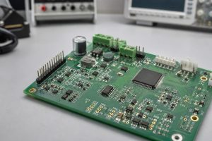
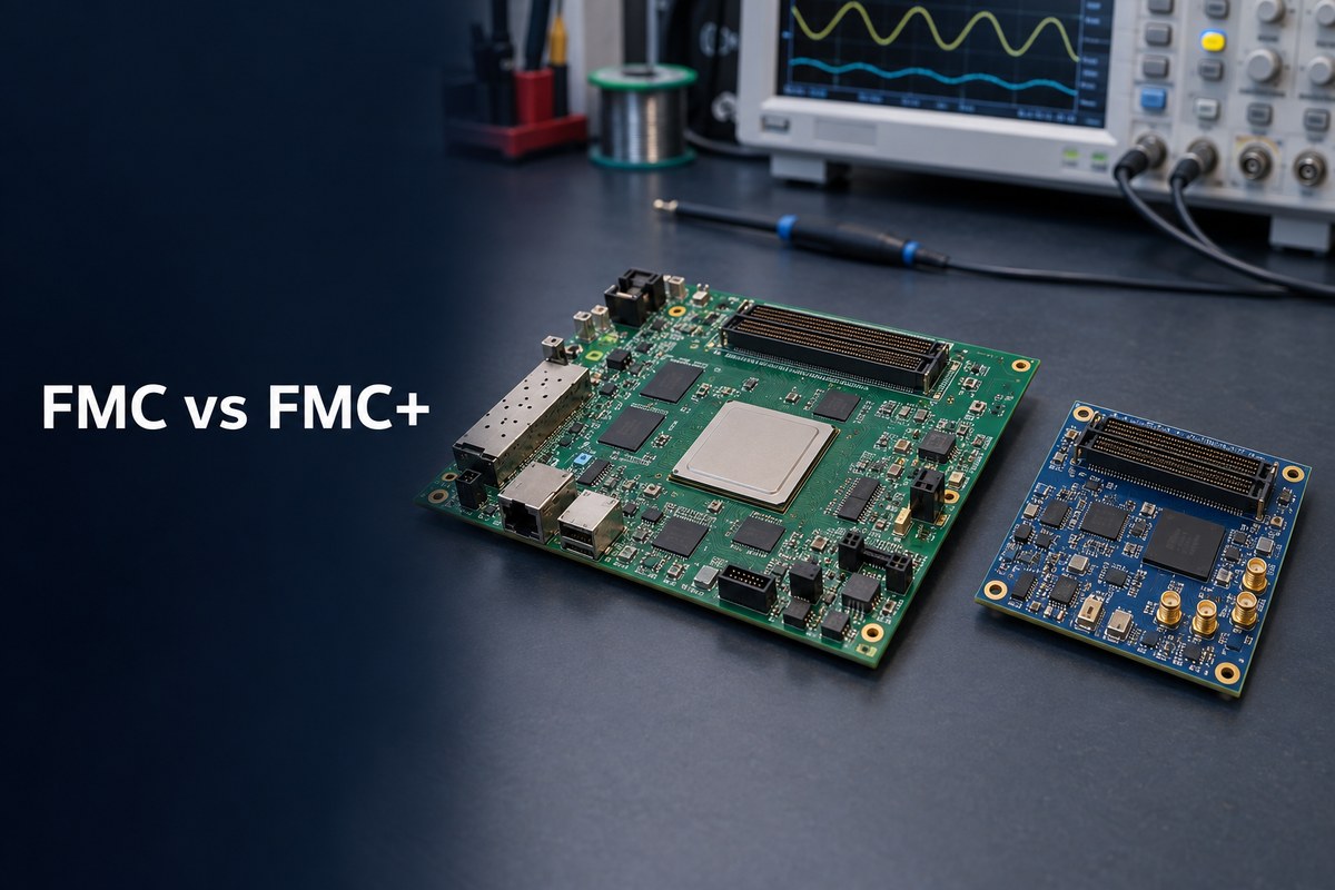
FMC vs FMC+ is primarily a comparison between the VITA 57.1 and VITA 57.4 FPGA mezzanine-card interfaces. Both connect an FPGA carrier board to a removable I/O module, but FMC+ supports more high-speed transceiver links and higher per-channel data rates. The choice affects connector compatibility, available FPGA I/O, carrier-board routing, mechanical clearance, and assembly requirements.
For a new carrier or mezzanine-board project, the important question is not simply whether FMC+ is “faster.” The interface must match the FPGA transceiver count, required bandwidth, existing cards, connector format, stack height, and manufacturing plan. EBest Circuit (Best Technology) can support customer-approved FMC and FMC+ designs with multilayer PCB fabrication, controlled-impedance production, connector assembly, inspection, and agreed PCBA testing. For a project review or quotation, contact sales@bestpcbs.com.
What Are FMC and FMC+?
FMC stands for FPGA Mezzanine Card. It is a modular interface defined by VITA 57.1 for connecting a carrier board to a smaller application-specific mezzanine card.
The carrier normally contains the FPGA, power architecture, memory, and system-level interfaces. The mezzanine card adds functions such as:
- analog-to-digital or digital-to-analog conversion
- RF transceiver channels
- high-speed data acquisition
- image or video interfaces
- optical or networking connections
- additional digital I/O
This separation allows one carrier platform to support different I/O cards without redesigning the complete FPGA board.
FMC+ is the enhanced interface defined by VITA 57.4. It retains the same basic carrier-and-mezzanine concept but expands the number and performance of multi-gigabit transceiver connections. It was developed for newer FPGA generations and converters that require more serial lanes and higher data throughput than the original FMC interface can provide.
FMC and FMC+ are therefore related standards, not two names for the same connector.
FMC vs FMC+: What Changes from VITA 57.1 to VITA 57.4?
The largest change is the high-speed serial capacity between the mezzanine card and the FPGA carrier.
| Feature | FMC / VITA 57.1 | FMC+ / VITA 57.4 |
|---|---|---|
| Common connector formats | LPC and HPC | HSPC and HSPCe |
| Maximum multi-gigabit transceivers | Up to 10 | Up to 32 |
| Typical maximum channel rate defined for the interface generation | Lower than FMC+ | Up to 28 Gbps per channel |
| Primary use | General FPGA I/O and moderate serial-lane counts | High-bandwidth converters, RF, imaging, networking, and data acquisition |
| Compatibility direction | FMC cards can be accepted by a suitable FMC+ carrier | FMC+ cards do not fit a standard FMC carrier |
The table describes interface capability, not guaranteed performance for every finished board. Actual speed still depends on the FPGA transceivers, connector option, PCB materials, routing length, reference-clock quality, via structure, and the complete channel budget.
FMC+ does not simply add more pins. It creates a more demanding high-speed interconnect between two independently manufactured PCBs. Both sides must use the correct connector footprint, pin mapping, stack height, signal assignment, and mechanical envelope.
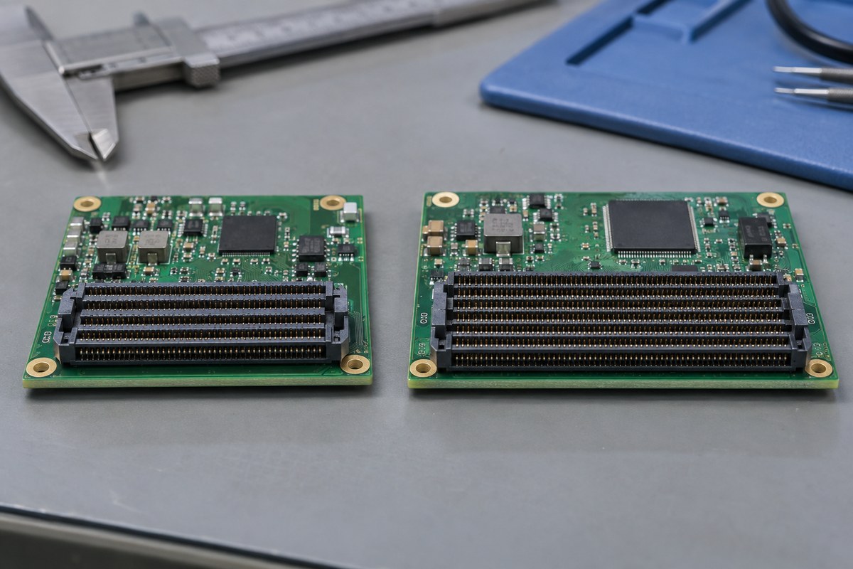
How Do the FMC LPC Connector and FMC HPC Connector Differ?
The original FMC standard commonly uses Low Pin Count and High Pin Count connector configurations.
FMC LPC connector:
- uses a reduced portion of the connector interface
- provides 34 differential user-I/O pairs
- provides one multi-gigabit transceiver link
- suits mezzanine cards that do not need the full FMC signal set
- can reduce routing demand on the carrier and mezzanine PCB
FMC HPC connector:
- uses the full high-pin-count interface
- provides 80 differential user-I/O pairs
- provides up to 10 multi-gigabit transceiver links
- supports higher I/O density and more complex mezzanine functions
- requires more signal breakout and routing resources
LPC and HPC are not only purchasing descriptions. The selected format controls which connector positions are populated and which signals the design can use.
FMC+ introduces the High Serial Pin Count connector family. A standard HSPC implementation supports more high-speed transceiver lanes than FMC HPC. The extended HSPCe arrangement adds another connector section so the interface can reach the full lane capacity defined by the standard.
The correct comparison is therefore:
- FMC LPC for lower I/O and serial-lane requirements
- FMC HPC for the full original FMC interface
- FMC+ HSPC when substantially more high-speed links are required
- FMC+ HSPCe when the design needs the extended interface capacity
The connector must be selected from the approved pinout and mechanical definition. A visually similar connector is not automatically electrically or mechanically interchangeable.
Is FMC+ Backward Compatible with FMC?
FMC+ provides useful backward compatibility, but only in one direction.
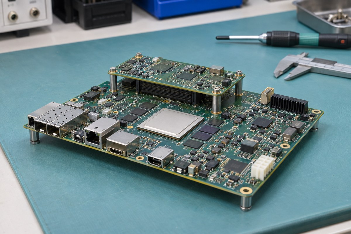
An FMC+ carrier with the appropriate female HSPC connector can accept many original FMC LPC or HPC mezzanine cards. Connector polarization and the shared interface region make this possible. This allows a newer carrier platform to continue using existing FMC I/O modules when its pin assignments, voltage settings, power limits, and mechanical clearances support them.
The reverse arrangement does not work. An FMC+ mezzanine card with a male HSPC connector cannot be installed on a standard FMC carrier. The FMC carrier lacks the full FMC+ connector structure and does not provide the additional high-speed interfaces expected by the card.
Backward compatibility must also be checked beyond physical fit:
- the carrier must support the mezzanine card’s VADJ requirement
- the assigned pins must match the carrier implementation
- required clocks and transceiver reference signals must be available
- the carrier must provide adequate power
- component height and front-panel geometry must not interfere
- FPGA firmware and system software must support the attached card
Physical insertion alone does not prove functional compatibility. The approved carrier and mezzanine documentation remains the controlling reference.
How Much More Bandwidth and I/O Does FMC+ Provide?
FMC+ provides its largest advantage when a design needs more high-speed serial lanes, higher lane rates, or both.
The original FMC HPC interface provides up to 10 multi-gigabit transceiver links. FMC+ increases this to 24 links in a common HSPC configuration and up to 32 with the extended HSPCe interface. FMC+ also supports lane rates up to 28 Gbps at the interface level.
That additional capacity can support applications such as:
- multi-channel high-speed ADC or DAC cards
- wideband RF and software-defined radio platforms
- high-resolution imaging and video acquisition
- optical networking interfaces
- test and measurement instruments
- data-converter development platforms
However, multiplying the lane count by the headline channel rate does not automatically give the usable application bandwidth. Encoding overhead, protocol efficiency, FPGA resources, converter interfaces, memory bandwidth, clocking, and thermal limits can all reduce the practical throughput.
The additional lanes also increase PCB complexity. More transceiver pairs must escape from the connector, remain within the channel-loss budget, cross as few discontinuities as practical, and reach the correct FPGA banks. FMC+ is most valuable when the system can use this capacity—not merely when the largest connector is available.
What Changes on an FMC+ Carrier Board PCB?
Moving from FMC to FMC+ increases the importance of the entire high-speed channel between the FPGA and the mezzanine card.
Connector placement and escape routing:
The HSPC connector must be positioned within the mechanical envelope while leaving workable routing space between the connector and FPGA. More transceiver lanes create greater breakout density. Connector orientation and pin assignment can determine whether the pairs can be routed without unnecessary layer changes or crossings.
Stack-up and material selection:
The customer-approved stack-up must support the required impedance, trace geometry, insertion-loss target, and PCB thickness. A design operating near the upper FMC+ data rate may need lower-loss laminate and tighter control than a lower-speed FMC board. Material decisions should follow the complete channel requirement, not the connector name alone.
Differential-pair routing:
High-speed pairs require controlled impedance, continuous reference planes, practical coupling, and limited discontinuities. The routing rules should define pair geometry, intra-pair skew, allowed via transitions, spacing from aggressors, and any length constraints required by the customer’s FPGA and channel analysis.
Via transitions and return paths:
Each connector or FPGA escape via adds discontinuity. Back drilling, blind vias, or other structures may be used when justified by the data rate, board thickness, and stub length. Ground stitching and uninterrupted reference paths help control return-current discontinuities around layer transitions.
Reference clocks and power integrity:
Reference clocks need clean routing and separation from noisy power-switching regions. The carrier must also deliver the required VADJ and other rails within the mezzanine card’s power limits. Additional I/O density can increase simultaneous switching and power demand, making plane structure and decoupling more important.
Mechanical fit:
The connector stack height, module dimensions, component keep-outs, mounting hardware, front-panel position, and cooling space must agree across both boards. An electrically correct layout can still fail integration if the installed mezzanine card contacts a heatsink, enclosure, cable, or tall carrier component.
These requirements should be defined in the released design package. EBest Circuit can review manufacturability, stack-up feasibility, impedance requirements, drill structures, copper clearances, and assembly access within the customer-approved electrical design.
What Makes FMC+ Connector Assembly More Demanding?
The FMC+ connector is a fine-pitch, high-density board-to-board interconnect. Its solder joints are largely hidden after assembly, so stable printing, placement, reflow, and inspection are more important than simple visual appearance.
Key manufacturing challenges include:
- maintaining PCB flatness beneath a long, dense connector array
- controlling solder-paste volume across all connector positions
- placing the connector accurately without disturbing nearby components
- supporting uniform reflow despite different copper and thermal conditions
- preventing opens, bridges, solder balls, or head-in-pillow-type separation
- protecting the connector from mechanical damage during handling
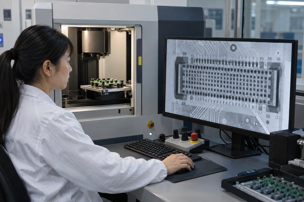
- verifying hidden solder joints after reflow
The paste aperture design, board finish, solder alloy, connector coplanarity, reflow profile, and local copper distribution all influence joint formation. A profile that works for smaller components elsewhere on the board may not automatically produce uniform joints under the FMC+ connector.
Inspection should match the hidden-joint risk. AOI can confirm connector presence, orientation, alignment, and visible edge conditions, but it cannot fully inspect every concealed connection. X-ray inspection can provide additional evidence of solder distribution, bridges, opens, and inconsistent joints. Electrical continuity or an agreed functional fixture may then verify the assembled interconnect at the required coverage level.
Inspection does not replace process control. The released footprint, stencil data, placement program, reflow settings, inspection criteria, and board revision should remain linked throughout the build.
Where Are FMC and FMC+ Used?
FMC and FMC+ are used where a carrier platform needs interchangeable, application-specific I/O close to an FPGA.
FMC remains suitable when the required interface fits within the LPC or HPC signal resources and the serial-lane rate is moderate. Typical examples include industrial I/O, control interfaces, lower-channel-count converters, instrumentation, and development platforms.
FMC+ becomes more attractive when the mezzanine card must transfer substantially more data to the FPGA. Common applications include:
- phased-array and wideband RF systems
- software-defined radio
- high-channel-count data acquisition
- high-speed ADC and DAC evaluation
- machine-vision and scientific imaging
- radar and electronic test equipment
- optical and high-speed networking development
- aerospace and defense signal-processing platforms
The same application category can use either standard. A data-acquisition card with a small number of moderate-speed converters may fit FMC HPC, while a card with many high-speed converters may require FMC+. The controlling factors are the actual lane count, data rate, I/O assignment, power, and mechanical requirements.
For PCB and PCBA production, the application also affects material selection, board thickness, layer count, impedance tolerances, surface finish, inspection coverage, and any functional-test arrangement. These details should be based on the released board specification rather than inferred from the words FMC or FMC+.
FAQs About FMC vs FMC+
Is FMC+ always better than FMC?
No. FMC+ provides more high-speed lanes and higher supported channel rates, but it can add connector, PCB, routing, and validation complexity. FMC remains appropriate when the application fits within LPC or HPC capacity.
Can an FMC card plug into an FMC+ carrier?
Yes, many FMC LPC and HPC mezzanine cards can plug into a properly implemented FMC+ carrier. Electrical, power, clock, pin-assignment, and mechanical compatibility must still be confirmed.
Can an FMC+ card plug into an FMC carrier?
No. The FMC+ HSPC connector and additional interface resources are not supported by a standard FMC carrier.
Does every FMC+ design operate at 28 Gbps per channel?
No. Twenty-eight gigabits per second is an interface capability. Actual operating speed depends on the FPGA, mezzanine device, PCB channel, connector option, materials, routing, and system implementation.
What should be controlled when manufacturing an FMC+ PCB assembly?
The released stack-up, controlled-impedance requirements, connector footprint, board thickness, mechanical tolerances, stencil design, placement, reflow profile, hidden-joint inspection, and agreed electrical testing should remain under revision control.
If you need PCB fabrication or PCBA support for a customer-approved FMC or FMC+ carrier/mezzanine design, send the released PCB data, BOM, stack-up and impedance requirements, connector part numbers, quantities, and inspection expectations to sales@bestpcbs.com. EBest Circuit can review the manufacturing scope and identify any DFM or assembly issues before production.