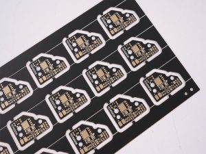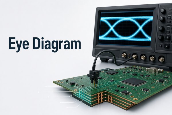
An eye diagram overlays many digital bit transitions in one time-domain display, making voltage margin, timing margin, noise, jitter, and intersymbol interference visible at a glance. A wide, tall opening usually indicates more receiver sampling margin. A narrow or closed opening shows that the channel, transmitter, receiver, or measurement setup is consuming that margin.
The picture is powerful, but it is not a complete root-cause report. Engineers must know where the waveform was captured, which data pattern and clock-recovery method were used, whether equalization was active, and which protocol limits apply before deciding whether a PCB channel is acceptable.
Eye Diagram Explained: What Does the Eye Opening Show?
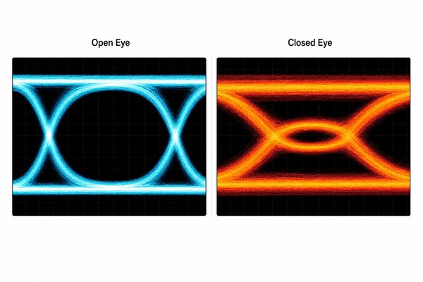
An eye opening shows the range of times and voltages in which a receiver can sample a symbol with lower risk of error. The oscilloscope folds repeated unit intervals onto the same horizontal window. Variations in transition time create horizontal spreading, while voltage variation creates vertical spreading.
This eye diagram explained in practical terms has three main regions:
- Upper and lower rails: the accumulated high and low voltage levels.
- Crossing region: the points where rising and falling transitions pass through the decision threshold.
- Eye opening: the central area that represents available timing and voltage margin.
For two-level NRZ or PAM2 signaling, one central eye is normally evaluated. Multi-level schemes such as PAM4 produce several vertically stacked eye openings, so level separation and linearity become additional concerns.
How Is an Eye Diagram Generated?
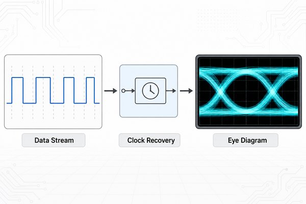
An eye diagram is generated by dividing a digital waveform into unit-interval segments and overlaying those segments on the same time axis. The waveform can come from a physical oscilloscope measurement, a measured channel response, or a circuit and interconnect simulation.
The displayed eye depends on more than the raw signal. The data pattern, sample depth, trigger, clock-recovery model, bandwidth, equalization, and measurement location all affect what appears on screen.
| Generation Method | Best Use | Main Limitation |
| Real-time oscilloscope | Capturing non-repetitive events and debugging live hardware | Instrument noise, bandwidth, memory depth, and probe loading affect the result |
| Sampling oscilloscope | Low-noise analysis of repetitive high-speed signals | Requires a repetitive signal and may miss non-repeating events |
| Channel simulation | Comparing stackups, routing, vias, connectors, and equalization before fabrication | Accuracy depends on the interconnect, package, buffer, and material models |
| BERT-based analysis | Measuring error behavior, bathtub curves, and low-probability timing events | Requires a defined pattern, receiver decision model, and suitable test access |
Triggering on the data can provide a quick view, but it may hide long runs without transitions and can suppress part of the signal jitter. A recovered clock is usually more representative, although its loop bandwidth determines how much jitter is tracked out. Compliance testing must therefore use the trigger and clock-recovery conditions required by the applicable interface specification.
How Do NRZ and PAM4 Eye Diagrams Differ?
NRZ, also called PAM2, uses two amplitude levels and normally produces one central eye opening. PAM4 uses four amplitude levels and produces three stacked eye openings, allowing each symbol to carry two bits but leaving less vertical separation between adjacent levels.
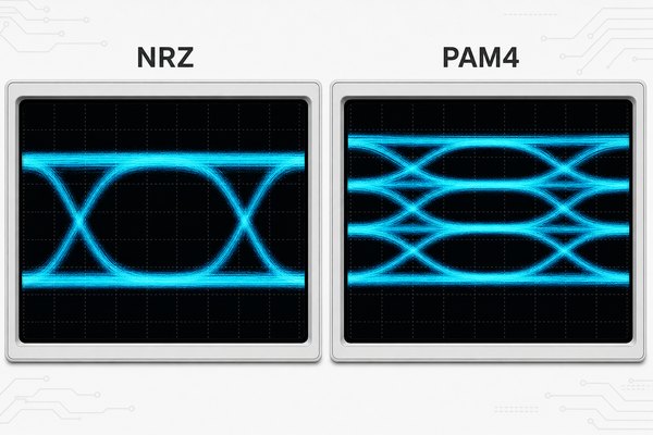
- NRZ/PAM2: one eye, two voltage rails, and one main decision threshold.
- PAM4: three eyes, four voltage levels, three decision thresholds, and additional concerns such as level separation and linearity.
- Measurement meaning: eye height, eye width, jitter, and noise remain important, but PAM4 requires each of its three openings to be evaluated.
- PCB impact: channel loss, reflections, crosstalk, and connector or via discontinuities consume already limited PAM4 voltage margin.
A reader should therefore confirm the modulation format before interpreting a screenshot. A single-eye rule or mask cannot be applied directly to a multi-level signal.
How Does Eye Diagram Signal Integrity Reveal Channel Margin?
Eye diagram signal integrity reveals how much electrical margin remains after a signal has passed through the transmitter, PCB traces, vias, connectors, cables, and receiver loading. Every discontinuity or loss mechanism can change the waveform that contributes to the final eye.
A more open eye generally means the receiver has a larger sampling window. A closing eye can indicate one or more of the following:
- Frequency-dependent channel loss has reduced the amplitude or slowed the edges.
- Impedance discontinuities have created reflections and ringing.
- Crosstalk or power noise has increased vertical noise.
- Clock or data jitter has shifted transition timing.
- Pattern-dependent loss has created intersymbol interference.
- Probe loading, cables, fixtures, or incorrect de-embedding have distorted the measurement.
The result should therefore be read as a combined view of the measurement point and test conditions. Comparing the transmitter output, channel output, and receiver input is more useful than treating one screenshot as a universal pass or fail.
Which Eye Diagram Measurements Matter Most?
Eye height and eye width are the fastest indicators of vertical and horizontal margin, but they should be interpreted with jitter, noise, crossing behavior, and edge-rate measurements. The exact measurement definitions can vary by oscilloscope software and protocol test package.
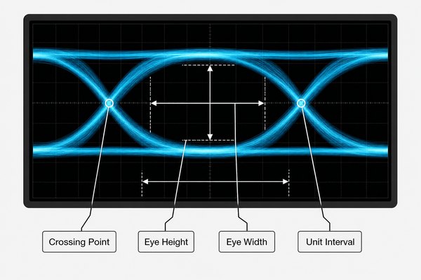
| Measurement | What It Shows | A Poor Result May Suggest |
| Eye height | Vertical voltage margin near the sampling region | Noise, attenuation, level compression, or rail variation |
| Eye width | Horizontal timing margin within a unit interval | Jitter, skew, ISI, or unstable clock recovery |
| Jitter | Variation in the timing of signal transitions | Clock noise, crosstalk, reflections, or pattern dependence |
| Crossing percentage | Balance and symmetry of rising and falling transitions | Duty-cycle distortion or asymmetric rise and fall behavior |
| Rise and fall time | Transition speed between logic levels | Bandwidth limitation, loading, or unequal channel response |
| Mask margin | Clearance from a protocol-defined forbidden region | Insufficient compliance margin under the specified test method |
No single value proves overall link reliability. A mask pass under the correct compliance setup is important, but system validation may also require jitter decomposition, bit-error-rate testing, TDR, or frequency-domain channel analysis.
What Causes an Eye Diagram to Close?
An eye closes when signal variations consume its vertical or horizontal opening. The most common causes are channel loss, reflections, noise, crosstalk, jitter, and intersymbol interference, but several effects can occur at the same time.
| Cause | Typical Eye Effect | Useful Follow-up Check |
| Insertion loss | Lower amplitude, slower edges, reduced eye height and width | Channel S-parameters, trace length, dielectric loss, and connector loss |
| Impedance mismatch | Ringing, multiple transition paths, or broadened crossings | TDR and discontinuity review at vias, pads, connectors, and terminations |
| Crosstalk or power noise | Thicker rails and reduced vertical opening | Aggressor activity, spacing, reference planes, and PDN noise |
| Timing jitter | Smeared edges and reduced horizontal opening | Clock source, PLL, power coupling, and jitter components |
| Intersymbol interference | Pattern-dependent edge locations and rail thickness | Data pattern, channel bandwidth, equalization, and loss profile |
| Measurement loading | Unexpected amplitude loss or distorted transitions | Probe bandwidth, probe capacitance, fixtures, cables, and de-embedding |
Start with the failure shape, then compare measurements at different channel locations. This avoids changing the PCB layout when the actual problem is a transmitter setting, receiver equalization state, fixture, or probe connection.
How Do Jitter, Noise, and ISI Change the Eye?
Jitter mainly reduces horizontal opening, noise mainly reduces vertical opening, and intersymbol interference can reduce both. In real systems, these effects overlap, so engineers should use the eye shape as a clue rather than a final diagnosis.
- Random jitter creates a distributed timing spread and has a statistical tail that depends on the observation depth.
- Periodic jitter can come from coupled switching regulators, clocks, or other repeating interference.
- Data-dependent jitter changes with the bit pattern and is often associated with bandwidth limits and ISI.
- Vertical noise thickens the high and low rails and reduces the voltage margin around the decision point.
- Duty-cycle distortion shifts rising and falling transitions differently, changing crossing position and eye symmetry.
Equalization can reopen an eye by compensating for channel loss, but too much equalization can amplify noise or create overshoot. Test transmitter settings and receiver settings separately before accepting the best-looking display as the final configuration.
Eye Diagram Test Setup
An eye diagram test setup needs a suitable data source, a defined data pattern, enough oscilloscope bandwidth and sample depth, a low-loading probe or fixture, and a repeatable clock-recovery method. The measurement point must also match the question being asked.
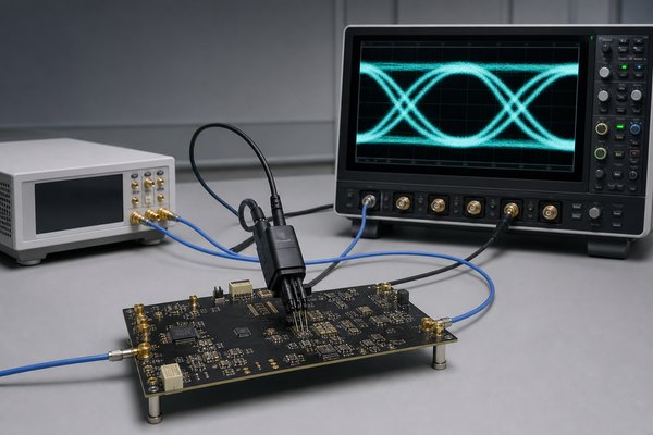
- Define the purpose. Separate transmitter characterization, channel evaluation, receiver stress testing, and system-level debugging.
- Select the pattern. Use the protocol-required pattern for compliance work or a pattern with enough transition and run-length content for design analysis.
- Choose the measurement point. Probe close to the transmitter for transmitter behavior and close to the receiver for channel-delivered behavior.
- Control the fixture. Keep cables, adapters, launches, and probe connections short and documented.
- Set clock recovery and equalization. Apply the method required by the interface specification rather than using an arbitrary display setting.
- Capture enough data. A shallow acquisition can hide rare timing or amplitude events.
- Save the setup with the result. Record data rate, pattern, bandwidth, probe, measurement point, equalization, clock recovery, and mask version.
A valid comparison changes one variable at a time. If the probe, pattern, acquisition depth, or equalization changes between captures, the apparent improvement may not come from the PCB revision.
How Should an Eye Mask Test Be Interpreted?
An eye mask test checks whether captured waveform samples enter a forbidden region defined for a particular interface and test method. A passing result means no disallowed mask hits were observed under those stated conditions; it does not mean every implementation has unlimited operating margin.
Before comparing mask results, confirm:
- The protocol, data rate, lane type, and test point are the same.
- The required reference receiver or equalization is applied.
- The clock-recovery model and bandwidth settings match the specification.
- The data pattern and acquisition depth are sufficient.
- Fixtures and cables are included, removed, or de-embedded consistently.
Mask limits are protocol-specific. A USB, Ethernet, HDMI, PCI Express, memory, or proprietary serial link cannot be judged with a generic mask borrowed from another interface.
Why Can a Clean Eye Still Miss Rare Errors?
A clean-looking eye can miss rare errors when the acquisition contains too few samples or the trigger excludes uncommon patterns. Random jitter has statistical tails, and low-probability events may not appear during a short capture. Eye diagrams and mask tests should therefore be paired with sufficient acquisition depth and, when the target error rate demands it, BERT or bathtub-curve analysis.
How Do PCB Stackup and Controlled Impedance Affect the Eye?
PCB stackup and controlled impedance affect reflections, propagation loss, crosstalk, and return-current continuity, all of which can change the eye opening. Trace geometry must be evaluated together with dielectric properties, copper thickness, reference-plane location, solder mask, and fabrication tolerances.
A practical stackup review should check:
- Target single-ended and differential impedance for each high-speed interface.
- Trace width, pair spacing, copper thickness, and dielectric height.
- Material loss characteristics across the relevant signal spectrum.
- Continuous reference planes beneath critical routes.
- Layer transitions and nearby return-path vias.
- Fabrication tolerances and an appropriate impedance coupon or test plan.
For a deeper manufacturing view, see our PCB stack-up and impedance control guidelines. Controlled impedance is necessary, but a nominal impedance target alone cannot compensate for excessive channel loss, long stubs, poor connector launches, or broken return paths.
How Do Vias, Connectors, and Differential Pairs Affect the Eye?
Vias, connectors, and differential-pair discontinuities can narrow the eye by adding loss, reflections, mode conversion, skew, or return-path interruption. Their impact rises as edge rates become faster and the structures occupy a larger electrical length.
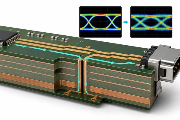
- Via stubs: an unused plated section can resonate and disturb the channel response. Backdrilling, blind vias, or a different layer transition may reduce the stub when the design justifies it.
- Reference changes: a signal changing layers needs a nearby return path. Missing return vias or stitching can create a larger current loop.
- Connector launches: pad geometry, anti-pads, ground pins, and breakout routing can create a localized impedance discontinuity.
- Differential skew: unequal electrical lengths convert part of the differential signal into common-mode energy and reduce timing margin.
- Pair spacing changes: inconsistent coupling changes differential impedance and can alter the eye.
Our articles on via effects in high-speed PCB design, differential signal PCB design, and high-speed PCB routing rules provide related layout checks.
How Should Engineers Run Signal Integrity Eye Diagram Analysis?
A useful signal integrity eye diagram analysis begins with a controlled baseline, then separates transmitter, channel, receiver, and test-fixture effects. Changing several variables at once may open the eye, but it does not identify the cause.
- Reproduce the failure. Save the exact data rate, pattern, lane, temperature, supply condition, and instrument setup.
- Check the measurement path. Verify probe loading, fixture quality, cable loss, calibration, clock recovery, and de-embedding.
- Compare measurement points. Capture near the transmitter and receiver when the design provides safe access.
- Classify the closure. Decide whether the dominant symptom is vertical noise, horizontal jitter, loss, ringing, skew, or pattern dependence.
- Correlate with another method. Use TDR for impedance discontinuities, S-parameters for channel loss, near-field checks for coupling, or BER testing for link performance.
- Change one variable. Adjust termination, equalization, route, via structure, connector launch, or power-noise source individually.
- Retest under the same conditions. Compare both the eye opening and the original failure mode.
PCB-level debugging should focus on the channel features that can physically create the observed symptom. Our guide to high-speed circuit board signal integrity covers the broader relationship between stackup, routing, return paths, loss, and verification.
FAQ About Eye Diagram Signal Integrity
Does a more open eye always mean a better design?
A more open eye usually indicates greater voltage and timing margin under the same measurement conditions. It is not a fair comparison if the data pattern, probe, clock recovery, equalization, bandwidth, or measurement point changed.
Can an eye diagram identify the exact PCB defect?
No. The eye shape can suggest loss, noise, jitter, ISI, or reflections, but TDR, S-parameters, probing at multiple locations, layout review, and component checks are often needed to locate the root cause.
What is one unit interval in an eye diagram?
One unit interval is the time allocated to one transmitted symbol. For two-level NRZ signaling, it corresponds to one bit period. Multi-level signaling can transmit more than one bit per symbol, so symbol rate and bit rate must not be treated as identical.
Is an eye mask the same for every high-speed interface?
No. The mask, reference receiver, test point, data pattern, clock recovery, and other conditions depend on the applicable protocol and compliance method.
Can simulation replace an oscilloscope eye measurement?
Simulation is valuable before fabrication and can predict how a channel may behave, but measured validation captures actual transmitter behavior, fabrication variation, connectors, packages, fixtures, noise, and receiver conditions. The two methods work best together.
How Can EBest Circuit Support High-Speed PCB Signal Integrity?
The eye diagram is most useful when the measurement conditions are controlled and the waveform is correlated with the physical PCB channel. At EBest Circuit, we have provided PCB and PCBA services since 2006. We support controlled-impedance PCB fabrication, PCB assembly, impedance testing, and engineering review for high-speed projects.
For a project review or quotation, send your Gerber files, stackup, impedance table, material requirements, BOM, assembly quantity, data rate, and any available eye-diagram or TDR results to sales@bestpcbs.com. We can review the manufacturing inputs and help align the board build with your verified signal-integrity requirements.