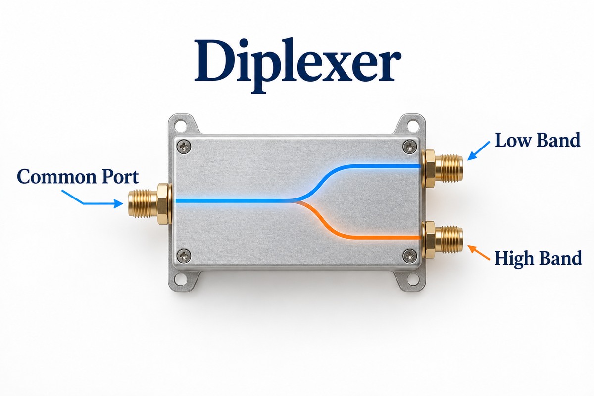
A diplexer is a passive, three-port RF network that combines or separates signals in two different frequency bands. One common port carries both bands, while two filtered ports route each band to its intended circuit. It allows an antenna or cable to serve two frequency ranges without using a broadband power splitter. The useful distinction is frequency-selective routing: a diplexer sends each band along a different path rather than dividing every signal between two outputs. Its performance depends on the passbands, insertion loss, isolation, impedance matching and the PCB connections around it.
Key Takeaways
- A diplexer has one common port and two frequency-selective branch ports; it can separate or combine two bands.
- A diplexer is not a broadband splitter. It does not inherently impose the ideal splitter’s 3 dB power division on each wanted signal.
- A duplexer separates transmit and receive paths; a diplexer separates frequency bands. The application and port specifications matter more than the name alone.
- Match the complete operating bands and system impedance. A 75Ω cable-network component is not a drop-in replacement for a 50Ω RF component.
- Insertion loss, return loss, isolation and power handling describe different requirements and must be checked separately.
- PCB stackup, ground connections, land patterns and connector launches can change the assembled circuit’s RF response.
- For a two-port VNA measurement, terminate the unused third port with the specified impedance and repeat measurements for the remaining paths.
What Is a Diplexer Used For?
A diplexer is used to share one RF connection between two frequency bands, such as separate wireless bands, GNSS bands or cable-network upstream and downstream bands.
- Wireless equipment: connect two band-specific circuits to a common antenna connection, provided the antenna supports both bands.
- GNSS receivers: separate selected satellite-navigation frequency ranges for their corresponding receiver paths.
- Cable networks: separate lower-frequency upstream signals from higher-frequency downstream signals.
- RF test and amplifier systems: combine different-band signals into a shared connection or separate them before measurement.
At EBest Circuit, we support the PCB and assembly work around these RF circuits. Our RF PCB manufacturing service can review the specified laminate, stackup and impedance requirements before fabrication. The diplexer itself remains a selected RF component or a customer-designed filter network.
How Does a Diplexer Work?
A diplexer works by presenting a low-loss path to the intended frequency band and a rejecting path to the other band at a shared junction.
A common arrangement uses a low-pass filter for the lower band and a high-pass filter for the upper band. Other designs use two band-pass filters. The filters must work together at the common port; joining two independently designed filters with a simple T-junction does not automatically produce a well-matched diplexer.
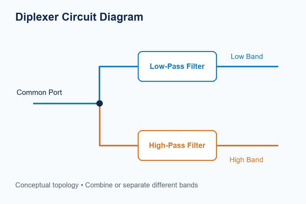
The diplexer circuit diagram above shows the routing concept, not a component-level circuit ready for fabrication. Actual implementations may use lumped inductors and capacitors, LTCC structures, distributed transmission lines or other resonant structures.
In a typical reciprocal passive network, signals can travel in either direction. A diplexer combiner therefore uses the two branch ports as inputs and the common port as the combined output. This does not translate frequencies: a 2.4 GHz input remains a 2.4 GHz signal.
What Is the Difference Between a Diplexer, Duplexer and Splitter?
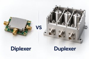
A diplexer separates frequency bands, a duplexer separates transmit and receive paths, and a splitter divides an input signal between outputs. For a closer look at TX/RX isolation and device selection, see our diplexer vs duplexer comparison.
| Device | Main function | Typical arrangement |
|---|---|---|
| Diplexer | Combine or separate two frequency bands | Common port, lower-band port, upper-band port |
| Duplexer | Isolate transmitter and receiver paths | Antenna, TX and RX ports; frequency-selective types use different TX/RX bands |
| Two-way splitter | Divide power across two outputs over its operating band | One input, two outputs carrying the same input spectrum |
An ideal equal two-way splitter sends half the input power to each output, corresponding to about 3 dB per path before excess loss. A diplexer does not make that equal division for an in-band signal; its wanted-path loss comes from the practical filter and interconnect.
The terms diplexer and duplexer sometimes overlap in commercial descriptions. TDK distinguishes multiband separation from TX/RX separation in its RF guidance. For a real design, check the port functions, passbands and required transmitter-to-receiver isolation rather than choosing by product name alone.
Which Diplexer Specifications Matter Most?
The essential specifications are passband limits, insertion loss, return loss, branch isolation, power handling and nominal impedance.
- Passbands: check both band edges, not only the center frequencies. A filter specified through 5.95 GHz should not be assumed to cover the entire 6 GHz Wi-Fi band.
- Insertion loss: measures attenuation through the wanted path. As a power calculation, 1 dB loss leaves about 79.4% of the input power at the output under matched conditions.
- Return loss: describes mismatch at a specified port. A 20 dB return loss corresponds to 1% reflected power at the measurement reference plane.
- Isolation: describes unwanted coupling between specified ports over specified frequencies. An illustrative 30 dBm input with 40 dB isolation produces −10 dBm leakage, which may still be excessive for a sensitive receiver.
- Power rating: check average and peak limits, temperature derating and any specified load-mismatch conditions.
- Impedance: use the component’s specified 50Ω or 75Ω environment, including measurement fixtures and terminations.
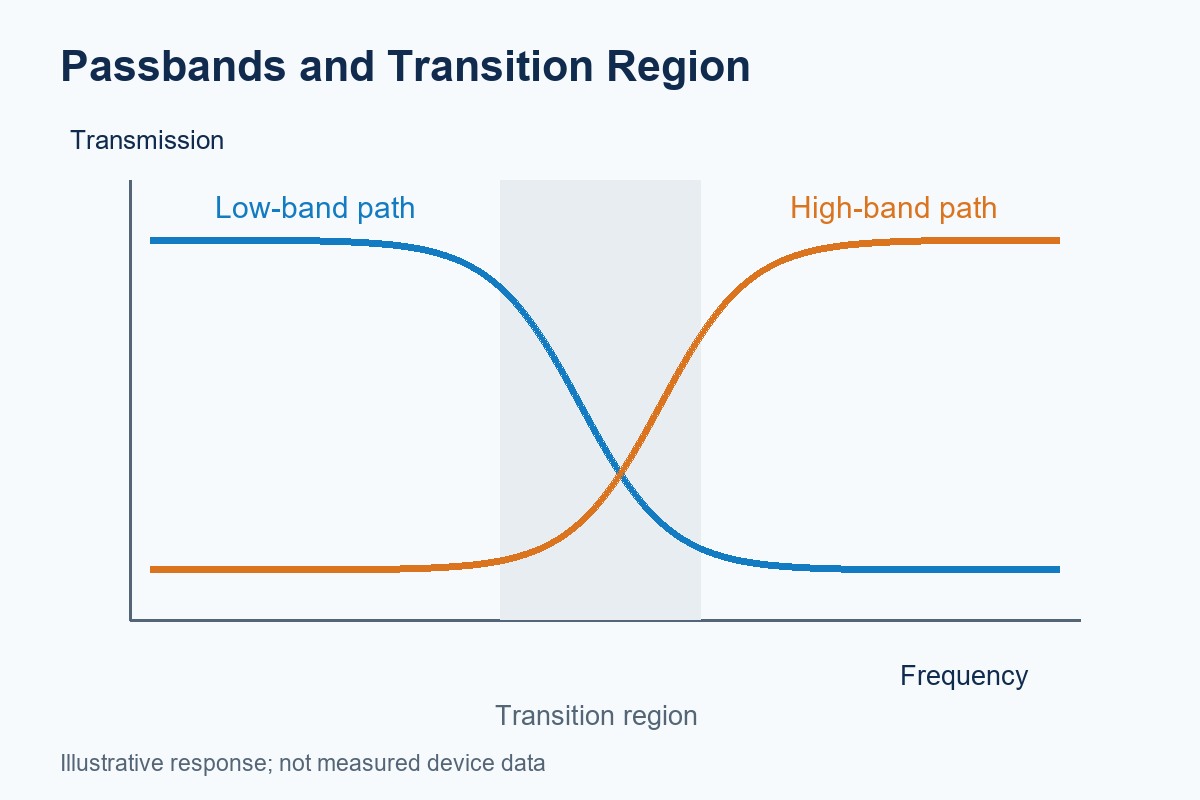
The transition region between usable bands must fit the system’s frequency plan. The illustration shows the principle only; component acceptance requires the manufacturer’s limits and measured response, not this conceptual curve.
Which Diplexer Filter Fits Your Frequency Bands?
The correct diplexer filter covers both required bands at the system’s nominal impedance and meets the loss, isolation and assembly requirements.
These published Mini-Circuits examples show why frequency range and impedance should be selected before package size:
| Model | Lower band | Upper band | Impedance | Implementation detail |
|---|---|---|---|---|
| DPGE-252-492R+ | 2400–2500 MHz | 4900–5950 MHz | 50Ω | LTCC, 2.0 × 1.25 mm package |
| DPLC-8510A0+ | DC–85 MHz | 102–1220 MHz | 75Ω | Datasheet states that it is not designed for reflow soldering |
The first example serves widely separated GHz bands; the second addresses a cable-network frequency split. They are not interchangeable. Likewise, a frequency range starting at DC does not establish every possible DC-feed connection: verify the pin-to-pin DC path and current rating before using a branch to power an active antenna or other device.
How Does Diplexer Design Affect PCB Layout?
Diplexer design affects PCB layout through the reference impedance, filter junction, grounding and parasitic coupling between the two branches.
For a packaged device, start with the exact manufacturer land pattern and evaluation-board layout. For a discrete filter, include the board stackup and component parasitics in the design model rather than treating the schematic as the complete RF circuit.
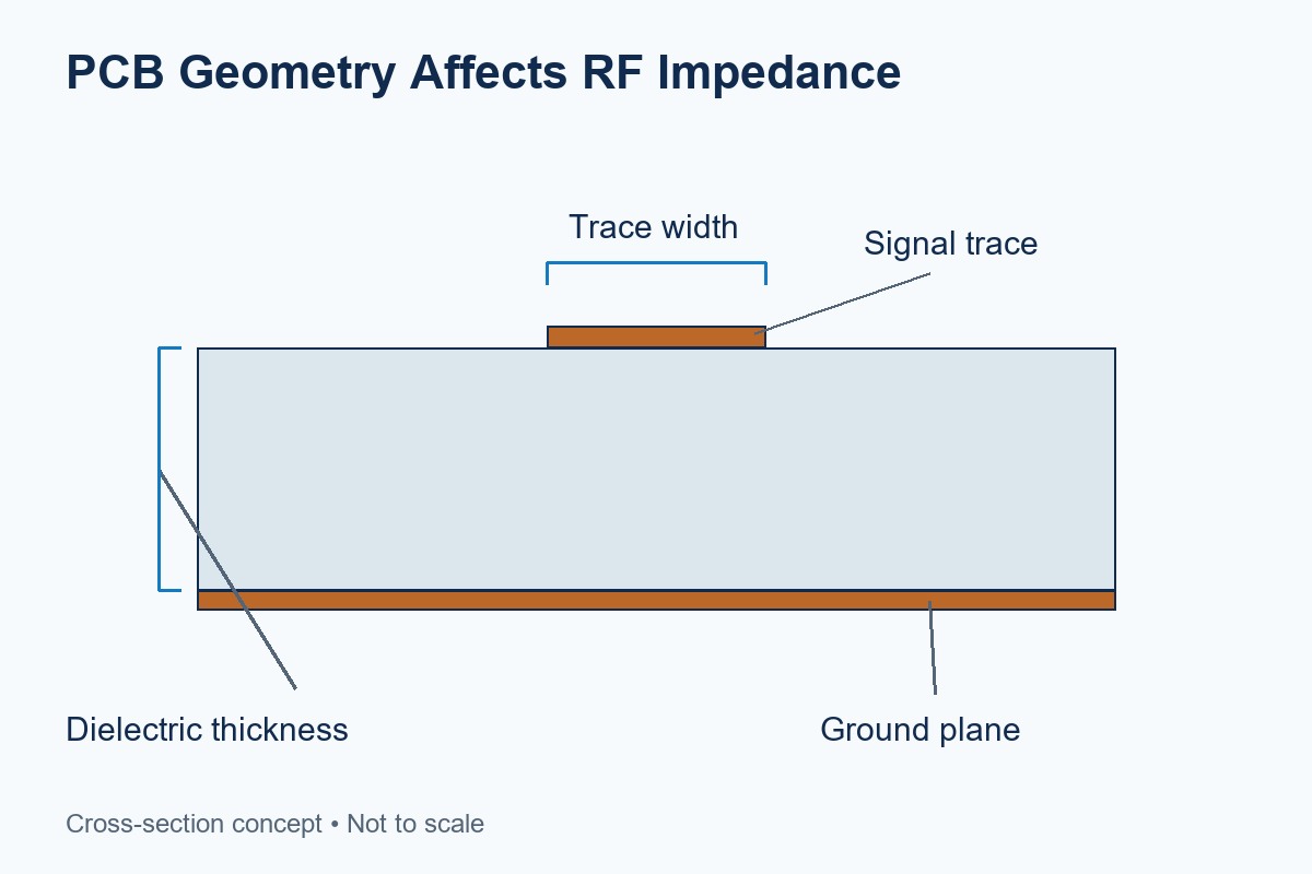
- Control the transmission-line geometry. Trace width depends on dielectric thickness, dielectric constant, copper thickness and the selected line structure. There is no universal 50Ω trace width.
- Keep a continuous return path. Avoid reference-plane splits beneath RF traces. Place ground connections and vias according to the component’s recommended layout.
- Limit coupling between branches. Avoid long parallel runs between the low- and high-band paths. Review spacing and shielding where the isolation budget is tight.
- Review connector launches. Connector pads, ground transitions and test-access stubs can introduce mismatch that is absent from the component datasheet.
- Preserve the approved stackup. Changes in dielectric thickness or laminate type can change impedance and filter behavior; review them before fabrication.
Our manufacturing review focuses on whether the specified material, copper features, stackup and assembly footprint can be reproduced. Circuit simulation and RF acceptance limits should remain tied to the actual design and selected components.
How Do You Test a Diplexer?
Test a diplexer with a vector network analyzer by measuring wanted-path insertion loss, port return loss and unwanted branch coupling across the required frequency ranges.
- Identify the common, low-band and high-band ports from the device drawing, not their physical position alone.
- Calibrate the VNA for the connection arrangement and reference planes. Account for adapters, cables and PCB fixtures.
- Connect two measurement ports to the common and low-band paths, and terminate the unused high-band port in the specified impedance.
- Repeat for the common-to-high-band path. Then measure branch-to-branch coupling with the common port terminated.
- Check return loss at each relevant port and compare the results with limits defined over frequency.
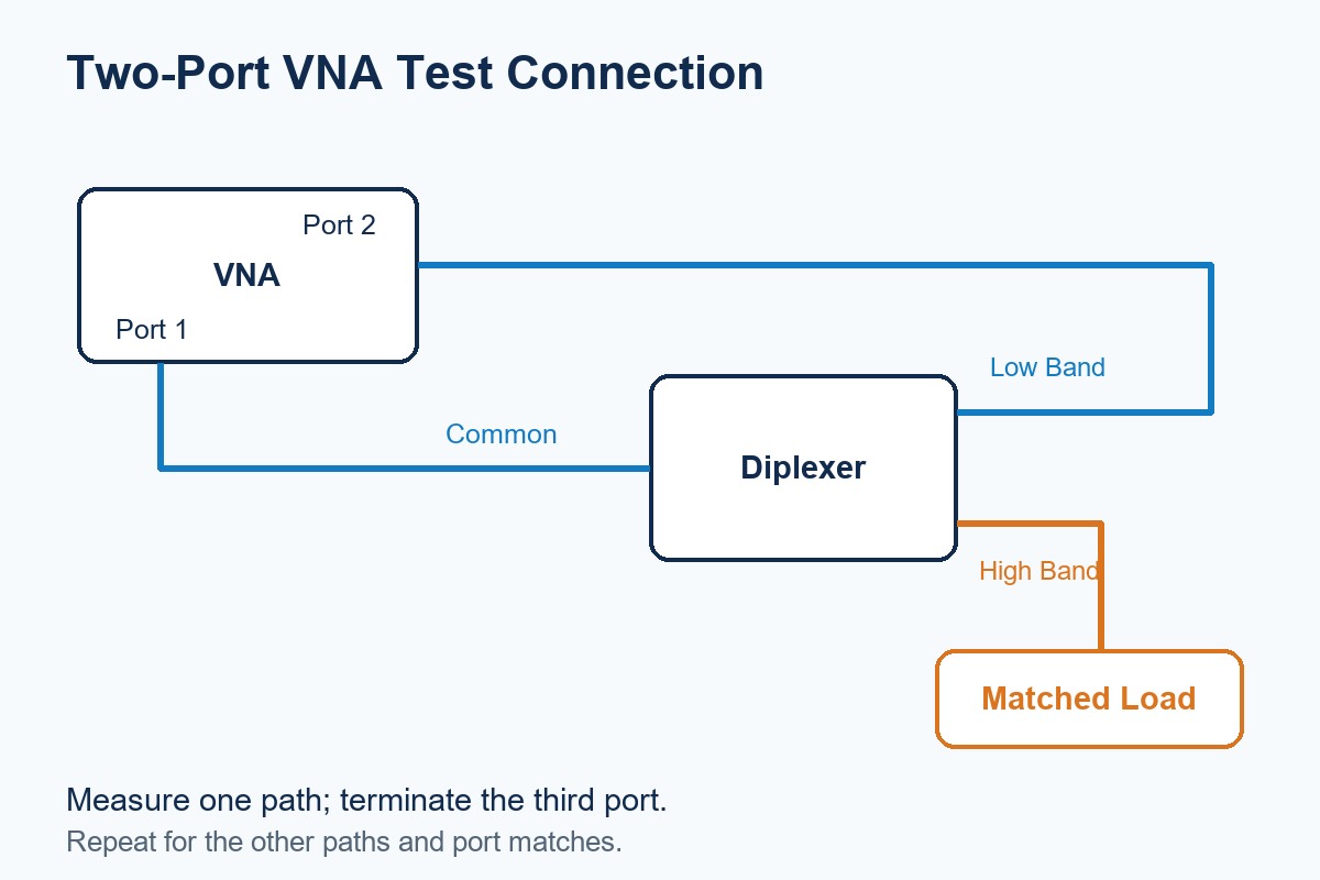
A multiport VNA can reduce reconnections. With either arrangement, measurement power must stay within the component and instrument ratings. Small-signal measurements alone do not establish high-power performance, thermal behavior or receiver protection under an actual transmitter load.
What Causes High Loss or Poor Isolation?
Unexpected loss or poor isolation commonly comes from incorrect port connections, impedance mismatch, layout coupling, assembly defects or an unsuitable measurement fixture.
- Loss increases near a band edge: check whether the operating frequency is outside the guaranteed passband.
- Both paths show poor matching: inspect the common-port launch, ground connections and calibration plane.
- Isolation is worse on the assembled board: investigate coupling around the filter, including parallel traces and shared return paths.
- Results change when cables move: check connector integrity, cable stability and calibration.
- Only some boards fail: inspect solder joints, component orientation and substitutions before changing the RF design.
For prototype troubleshooting, compare the board with the manufacturer’s evaluation arrangement where available. This helps separate component behavior from PCB and fixture effects.
FAQ About Diplexers
Can a diplexer separate two signals at the same frequency?
No. Its routing is frequency-selective, so it cannot distinguish two signals occupying the same frequency solely because they come from different sources.
Does a diplexer need a power supply?
A conventional passive diplexer does not need a separate supply. A larger module may include powered switches or amplifiers, which must be checked separately.
Can a diplexer circuit use FR-4?
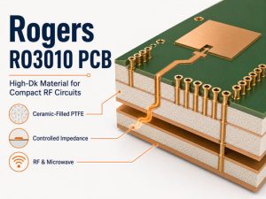
Yes, when the selected FR-4 system, routing length and frequency meet the circuit’s loss and impedance requirements. Higher-frequency or tighter-loss designs may require a lower-loss laminate; there is no single frequency cutoff for every board.
What is the difference between a diplexer and a triplexer?
A diplexer separates two bands using three ports. A triplexer separates three bands and typically has one common port plus three band-specific ports.
What is the difference between a circulator and a diplexer?
A circulator routes signals between ports in a defined nonreciprocal sequence. A conventional diplexer routes signals according to frequency and is generally reciprocal.
How Can EBest Circuit Support Your RF PCB Project?
We support RF PCB fabrication and PCB assembly for customer-designed circuits, including boards that integrate diplexers and associated RF components.
For these projects, our review can address the specified laminate and stackup, impedance-controlled routing requirements, component footprints and assembly constraints. Identify any components that cannot follow the standard reflow process before production. RF test methods, fixtures and acceptance limits should be agreed as part of the project scope.
Contact sales@bestpcbs.com to discuss your RF board. Share the board files and selected diplexer datasheet so we can review the manufacturing and assembly requirements with your team.