Creepage vs clearance describes two different distances between conductive parts on a PCB: the shortest route along an insulating surface and the shortest route through air. The difference becomes clear when you cut a slot between two pads. The surface route may become longer, while the direct air gap stays the same.
Those distances must also survive manufacturing and assembly. EBest Circuit provides PCB fabrication, assembly, and DFM support for features such as specified laminates, isolation slots, and component spacing. Discuss your PCB or PCBA requirements with our team at sales@bestpcbs.com.
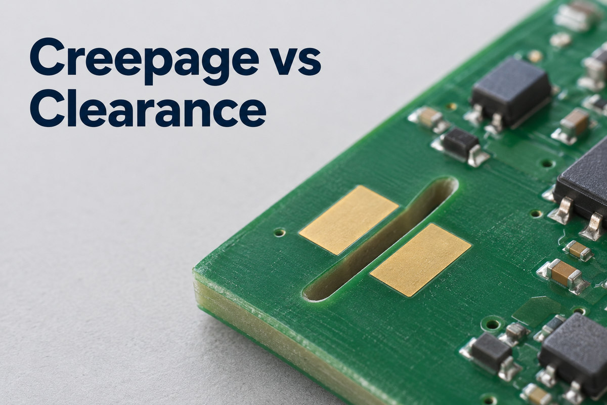
Creepage vs Clearance: What Is the Difference?
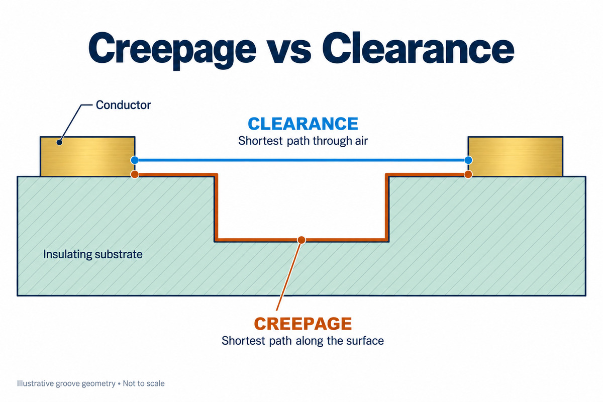
Creepage follows an insulating surface. Clearance passes through air. They describe different paths and address different electrical failure mechanisms.
| Comparison | Creepage | Clearance |
|---|---|---|
| Where it is measured | Along an insulating surface | Through air |
| Typical failure concern | Surface tracking | Air breakdown and arcing |
| What a through-slot may change | Lengthens the surface route | May leave the direct air gap unchanged |
On a simple, flat PCB:
- Surface route: Follow the insulating board surface from one exposed pad edge to the other.
- Air route: Find the shortest path through air between the same conductive parts.
- Possible result: The distances can be equal when no feature changes either route.
The risks are different. Electrical stress, moisture, and contamination can damage an insulating surface and create a conductive track. An air gap can instead break down when it cannot withstand the applied electrical stress.
The material between internal copper layers is solid insulation. Its thickness is a separate consideration, rather than an air gap or a surface creepage path.
How Are Creepage and Clearance Measured on a PCB?
Measure from conductive edges, not pad or pin centers. Then identify the shortest qualifying path for each distance.
Three measurement rules:
- Use the actual conductive boundary. On a bare board, this may be a pad edge. After assembly, a lead or solder joint may be closer to the neighboring conductor.
- Follow the correct route. Clearance passes through air; creepage follows the insulating surface under the applicable measurement rules.
- Compare alternative paths. A nearby slot end, board edge, or component housing may provide a shorter route than the one first noticed.
Example: two pads near a slot end:
The route around the nearby end is shorter than the route around the far end. Measuring the longer route overstates the available creepage distance. Making the far end longer may therefore provide little benefit.
CAD tools help check modeled copper spacing and, where supported, surface paths. The assembled product still needs consideration because a board-only model may omit leads, solder, and mounting hardware.
What Determines the Required Creepage and Clearance?
Available distance is a physical measurement. Required distance depends on the electrical conditions and applicable standard. Voltage alone does not determine both requirements.
| Creepage depends strongly on | Clearance depends strongly on |
|---|---|
| Working voltage across the insulation | Relevant impulse, transient, and peak voltage stresses |
| Pollution conditions at the insulating surface | Air conditions, including operating altitude |
| Material group and resistance to tracking | Applicable withstand and environmental requirements |
Material effect:
A material's comparative tracking index, or CTI, describes its resistance to surface tracking. A higher-CTI material may permit a smaller required creepage distance under the applicable rules. It does not increase the physical air gap.
Altitude effect:
Lower air pressure can require increased clearance. Changing the laminate's CTI does not compensate for an air gap that is too small for the operating conditions.
Requirements that apply to both:
- Insulation function: Functional, basic, and reinforced insulation serve different purposes.
- Equipment standard: Product-specific requirements establish the applicable conditions and acceptance criteria.
IEC 60664-1 provides an insulation-coordination framework. A spacing calculator can help apply a defined rule set, but its assumptions must match the product; entering only a voltage cannot establish every insulation requirement.
How Do PCB Slots Increase Creepage Distance?
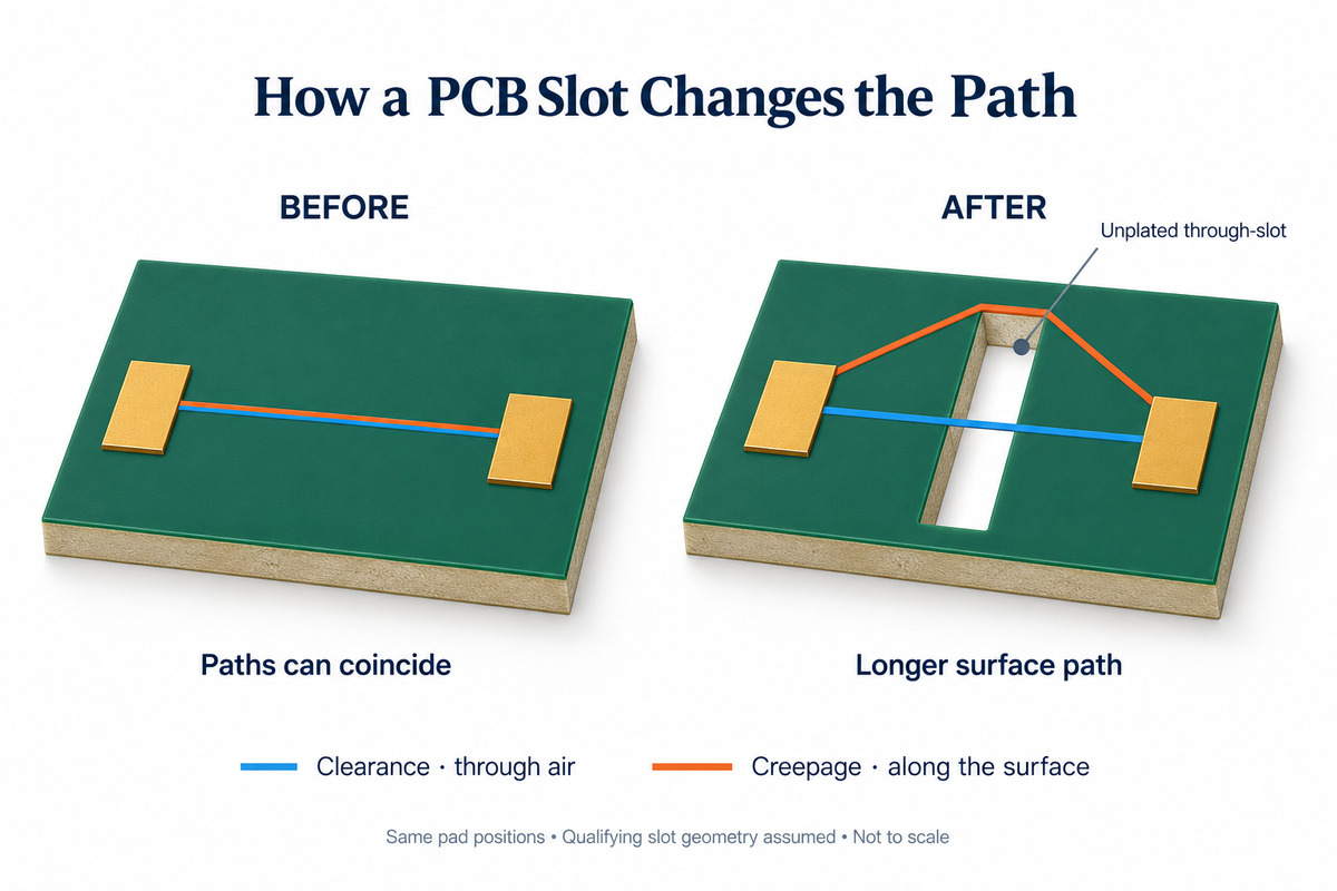
A qualifying through-slot makes the surface path go around an opening without necessarily increasing the air gap.
| Between the same fixed pads | Before the slot | After the slot |
|---|---|---|
| Surface path | Runs directly across the board surface | Must go around a slot end, if the opening qualifies under the measurement rules |
| Direct air path | Crosses the gap between the pads | Can still cross the opening directly |
| Practical effect | Surface and air distances may be equal | Creepage may increase while clearance remains unchanged |
What determines whether the slot helps:
- Position and length: The slot must lengthen the shortest surface route, not simply add machining elsewhere.
- Width: The applicable rules determine whether the opening can be counted and how its contour is measured.
- Other surface paths: A component housing spanning the slot may provide a shorter route.
- Finished geometry: Routing position and end radius affect the actual distance around the slot.
A blind groove retains a floor, so it cannot automatically be measured like a through-slot. Likewise, a plated slot contains conductive material and cannot be treated as an unplated isolation opening.
How Do Solder Mask and Conformal Coating Affect Insulation Spacing?
Neither treatment automatically permits smaller spacing. Its role depends on the protected area and the qualification of the insulation system.
| Treatment | What it does | What still matters |
|---|---|---|
| Solder mask | Covers selected copper while leaving soldering areas exposed | Exposed pads, openings, and terminations remain part of the insulation geometry |
| Conformal coating | Protects selected assembly surfaces from environmental exposure | Coverage and qualification determine whether different spacing treatment is permitted |
For a coating system, the important details include:
- Coverage around component leads and edges.
- Adhesion and curing.
- Uncoated areas along the relevant insulation path.
- Qualification under the applicable requirements.
IEC 60664-3 addresses pollution protection through coating, potting, or moulding. A suitably qualified system may allow different spacing treatment, but simply seeing a coating on the board is insufficient.
Example: an uncoated connector area:
If the limiting path passes through that area, coating the rest of the board does not resolve it. Any reduced-spacing allowance must apply to the actual protected path. The coating also does not physically move metal contacts farther apart.
Why Can PCB Assembly Reduce Insulation Spacing?
The closest conductive surfaces after assembly may be closer together than the bare-board pads. Components can also introduce new surface paths.
| Assembly feature | Possible effect |
|---|---|
| Solder extending beyond a pad | Moves the conductive boundary closer to a neighboring conductor |
| Bent or protruding lead | Reduces an air gap above or below the board |
| Component housing across a slot | Provides another surface path between leads |
| Screw or metal standoff | Introduces another nearby conductive object |
| Placement variation | Changes the minimum separation between parts |
Example: a component mounted across an isolation slot:
The PCB surface route may be long enough, but the component's leads or housing can create a shorter path. The board and component must therefore be considered together.
Two production concerns should remain separate:
- Dimensions: Copper edges, slot position, placement, and solder-joint shape determine the finished geometry. Nominal dimensions need allowance for applicable production tolerances.
- Cleanliness: Residue or contamination can increase leakage risk even when the measured spacing remains unchanged.
This is why fabrication details and assembly conditions belong in the same discussion as the layout. A correct copper-spacing value alone does not describe every path on the finished PCBA.
FAQs About Creepage and Clearance
Can creepage be less than clearance?
For the same conductive parts and exposed insulation geometry, creepage is normally equal to or greater than clearance. A smaller creepage value in a requirements table does not override the associated clearance requirement.
Can creepage and clearance be equal?
Yes. They can be equal on a flat, uninterrupted insulating surface. Each must still satisfy its applicable minimum requirement.
Is pin pitch the same as clearance?
No. Pitch is generally measured center to center. Clearance is measured between conductive surfaces, so lead width, shape, and solder affect the available gap.
Does the same voltage always require the same spacing?
No. Materials, pollution conditions, altitude, transient exposure, and insulation function can change the requirements.
Does passing a hipot test prove creepage and clearance compliance?
No. It demonstrates withstand performance under specified test conditions. It does not establish compliance with every dimensional or environmental requirement. Any alternative acceptance method must be permitted by the applicable standard.
Understanding creepage vs clearance helps connect the PCB layout with the finished assembly. EBest Circuit supports DFM review, PCB fabrication, and assembly around your specified materials and insulation-spacing requirements. Send your project details to sales@bestpcbs.com.