A copper direct-thermal-path MCPCB gives a high-power LED a shorter route from its thermal pad into the metal base. That reduction can preserve junction-temperature margin when a conventional insulated metal substrate becomes the dominant thermal bottleneck. The board is only one part of the system, however. Package compatibility, copper-pedestal geometry, solder quality, interface material, heatsink design, mounting pressure, ambient temperature, and airflow must all support the same thermal target.
This guide explains how to make that decision without relying on a universal wattage threshold. It also shows what to calculate, what to specify on the fabrication drawing, what to inspect during assembly, and how to validate the finished LED module before release.
What Is a Copper Direct-Thermal-Path MCPCB and How Does It Work?
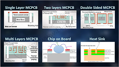
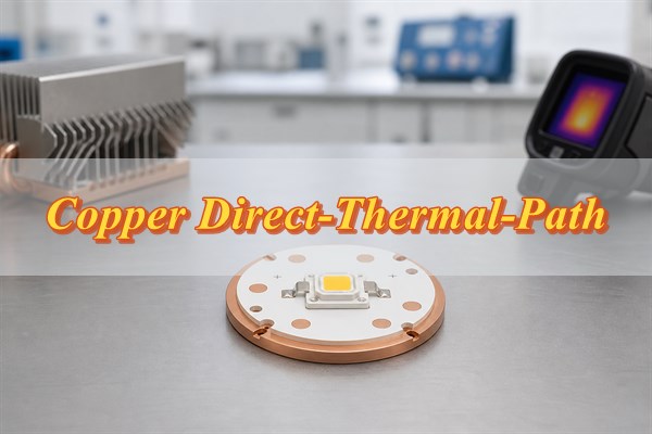
A Cu-DTP board places a controlled copper feature directly beneath the LED thermal pad, bypassing the dielectric in the primary heat path. In a conventional aluminum MCPCB, heat normally travels from the LED thermal pad through solder, copper foil, an electrically insulating dielectric, and then the aluminum base. The dielectric is thin, but its thermal conductivity is far below that of copper, so it may contribute a large share of the board-level thermal resistance.
In a direct-thermal-path construction, a copper pedestal or coin reaches the component-side thermal land. The LED thermal pad is soldered to this feature, allowing heat to enter the metal base without first crossing the dielectric. The surrounding signal and power pads remain on insulated circuitry. This structure improves the vertical heat route at the source while preserving electrical routing elsewhere on the board.
The word “direct” does not mean the complete module has zero thermal resistance. The remaining path still includes the LED package, solder joint, copper feature, baseplate, thermal interface material, heatsink, and convection or radiation to the environment. The practical benefit is the removal of one high-resistance layer from the most concentrated part of that path.
| Heat-Path Element | Conventional Aluminum MCPCB | Cu-DTP MCPCB |
| LED thermal pad | Soldered to surface copper | Soldered to a controlled copper pedestal |
| Dielectric position | Inside the primary vertical heat path | Kept outside the direct pedestal path |
| Electrical isolation | Provided continuously beneath the circuit layer | Must be defined around the pedestal and routed pads |
| Main design benefit | Simple, economical insulated-metal construction | Lower source-to-base resistance at high heat flux |
| Main review risk | Dielectric thermal resistance | Pad compatibility, pedestal geometry, and process control |
When Should You Choose a Copper Direct-Thermal-Path MCPCB Instead of an Aluminum MCPCB?
Choose Cu-DTP when the calculated junction-temperature margin cannot be met reliably after the conventional MCPCB dielectric and realistic interface losses are included. LED electrical input power alone is not a sufficient selection rule. Two modules operating at the same wattage may have very different heat flux, emitting area, ambient temperature, optical efficiency, enclosure geometry, and airflow.
Start with the complete thermal system. Treat the board, interface material, heatsink, enclosure, and airflow as one thermal system. A direct path is most valuable when the thermal source is concentrated, the package exposes a suitable thermal pad, the allowable temperature rise is small, and the heatsink can actually remove the heat delivered to it. If the external heatsink is already inadequate, lowering only the board resistance may move heat into a base that remains too hot.
- Limited junction margin: The predicted maximum junction temperature is too close to the LED manufacturer’s limit after tolerances and worst-case ambient are included.
- High local heat flux: A compact emitter or tightly spaced LED cluster concentrates heat into a small board area.
- Dielectric-dominated loss: The standard MCPCB dielectric consumes an unacceptable share of the allowable board-to-heatsink resistance.
- Optical stability requirement: The application needs tighter control of output, color, or electrical behavior over temperature.
- Restricted cooling: A sealed enclosure, elevated ambient, limited airflow, or compact heatsink leaves little system-level margin.
A conventional aluminum MCPCB remains appropriate when its measured thermal performance meets the requirement with adequate production margin. Cu-DTP adds fabrication and assembly controls, so it should solve a quantified thermal problem rather than serve as a default material upgrade.
How Can You Confirm That an LED Package Is Compatible With a Direct Copper Thermal Path?
Compatibility depends first on the electrical function of the exposed thermal pad, not on LED power or package size. The copper pedestal may be electrically connected to the metal base or another defined potential. If the LED thermal pad is internally connected to an anode, cathode, or sensitive node, placing it on a shared conductive pedestal can create a short circuit or an unintended common connection.
Review the LED datasheet, package drawing, recommended land pattern, and electrical schematic together. Confirm whether the thermal pad is electrically neutral, internally connected, or required to remain isolated. For an array, check whether multiple emitters can share the same base potential. A package that works on one isolated pedestal may be unsuitable for several LEDs tied to a common copper base.
- Identify the pad: Match every bottom-side land in the package drawing to its electrical and thermal function.
- Confirm potential: Determine whether the exposed pad is floating, anode-connected, cathode-connected, or otherwise restricted.
- Check the circuit: Verify that the planned base and pedestal potential is compatible with series, parallel, or independently driven LEDs.
- Review isolation: Define the required spacing between the pedestal, routed copper, mounting hardware, and heatsink.
- Test continuity: Add an electrical isolation or continuity check that proves the manufactured board matches the intended connection scheme.
Do not approve the construction based only on a footprint library name. The exact ordering code and revision of the LED package must be part of the review because pad functions can differ within a product family.
How Do You Calculate the LED Junction-Temperature and Thermal-Resistance Budget?
Calculate the maximum allowable junction-to-ambient resistance from the worst-case temperature rise and the heat that must be dissipated. A useful first estimate is RθJA,max = (TJ,target – TA,max) / Pheat. Here, TJ,target is the selected design target rather than the absolute maximum rating, TA,max is the worst expected ambient temperature, and Pheat is the input power converted to heat.
Separate the available total resistance into the portions controlled by the package, board, interface, heatsink, and surrounding air:
RθJA = RθJ-PAD + RθPAD-BASE + RθTIM + RθHS-A
The labels must match the LED manufacturer’s defined measurement points. A published junction-to-case or junction-to-solder-point value is valid only when the temperature is measured at the specified reference location. Moving the thermocouple farther from the package can understate the estimated junction temperature because the measured board temperature is lower.
| Budget Input | Required Definition | Common Error |
| Junction target | Design value with reliability and performance margin | Using the absolute maximum as the normal target |
| Maximum ambient | Temperature at the module’s real installation location | Using room temperature for an enclosed product |
| Heat dissipation | Electrical input minus emitted optical power when reliable data is available | Treating rated electrical power as a universal heat value without stating the assumption |
| Package resistance | Datasheet value tied to the specified reference point | Mixing junction-to-case and junction-to-solder-point definitions |
| Board and interfaces | Worst-case manufactured and assembled values | Using ideal material conductivity without contact resistance |
| Heatsink to ambient | Characterized at the actual orientation and airflow | Using a catalog value from different cooling conditions |
A one-dimensional resistance network is useful for screening and budget allocation. It becomes less reliable for clustered LEDs, nonuniform boundaries, lateral spreading, several material regions, or heat leaving through multiple surfaces. Use a suitable thermal model and prototype measurements when geometry makes the simple network inconclusive.
Which Copper Direct-Thermal-Path MCPCB Specifications Affect Thermal Performance?
The specification must control the complete heat path, not merely call the board “Cu-DTP.” A fabrication drawing should identify the base material, base thickness, circuit copper, dielectric system outside the pedestal, pedestal material and dimensions, surface finish, isolation boundaries, outline, flatness, and the dimensions that require inspection.
- Base material and thickness: Define the copper grade or approved equivalent and the finished base thickness that supports spreading, stiffness, and mounting.
- Circuit copper: Specify finished copper thickness and current requirements for the LED power paths.
- Dielectric system: Identify where insulation remains necessary and define its approved material rather than assuming it is irrelevant.
- Pedestal geometry: Control the top size, height, location, and relationship to the finished board surfaces.
- Surface finish: Select a solderable finish compatible with the LED termination, assembly process, storage period, and reflow profile.
- Flatness and thickness: Set values that allow uniform TIM contact and predictable mounting pressure across the module.
- Inspection features: Mark critical dimensions and electrical-isolation points so acceptance does not depend on a generic drawing note.
Material thermal conductivity is not a complete board specification. The effective resistance depends on the actual path length, area, interfaces, and manufactured geometry. Ask the supplier to confirm the proposed construction and controlled dimensions during DFM instead of relying on a trade name alone.
How Should the LED Thermal Pad and Copper Pedestal Be Designed?
The thermal land and copper pedestal must overlap consistently after fabrication and assembly tolerances are applied. The package land pattern defines solderable geometry, while the pedestal defines the direct heat-transfer area. If the two features are poorly registered, part of the thermal pad may sit over dielectric, solder mask, or a step in the surface.
Begin with the LED manufacturer’s recommended land pattern. Create a tolerance stack that includes package placement, copper imaging, pedestal machining or forming, layer registration, solder-mask registration, and any dimensional change during fabrication. The minimum guaranteed overlap—not the nominal CAD overlap—should carry the required heat flow.
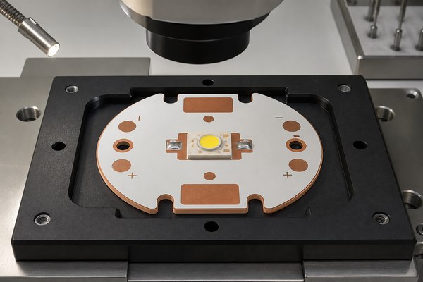
- Thermal-land size: Follow package guidance unless a validated assembly study supports a controlled modification.
- Solder-mask clearance: Prevent mask encroachment without creating an unnecessarily large exposed region.
- Pedestal top area: Support the thermal pad while maintaining required clearance from electrical lands.
- Surface coplanarity: Avoid a step that tilts the package or changes solder thickness across the terminations.
- Paste definition: Use a stencil pattern that controls solder volume and gas escape for a large thermal land.
- Inspection access: Plan X-ray, cross-section, continuity, or dimensional evidence for features that are hidden after assembly.
The design review should place the package drawing, paste layer, mask layer, copper land, pedestal boundary, and tolerance limits in one overlay. That comparison is more useful than reviewing each file separately.
How Is a Copper Direct-Thermal-Path MCPCB Manufactured and Controlled?
Manufacturing must form a repeatable direct copper feature while preserving insulation and coplanarity around the routed circuit. The exact sequence depends on the supplier’s qualified construction, but the control objectives remain the same: locate the pedestal accurately, bond or integrate the surrounding insulated circuit, finish the soldering surface, machine the outline, and verify electrical and dimensional acceptance.
- Review the construction: Confirm the pedestal concept, insulation boundary, material compatibility, and inspection plan before production data is released.
- Prepare the metal base: Form or machine the controlled copper feature using the supplier’s qualified method.
- Build the insulated circuit: Laminate or otherwise integrate the dielectric and circuit copper around the direct path without contaminating the pedestal surface.
- Image and etch circuitry: Create the LED power and signal features while maintaining clearance from the conductive base feature.
- Finish exposed lands: Apply the specified solderable finish with controlled coverage and thickness.
- Machine the board: Complete the outline, mounting holes, and thickness controls without distorting the contact surface.
- Inspect critical features: Measure pedestal position, top geometry, board thickness, flatness, surface condition, and electrical isolation.
A supplier may use different proprietary process details, so the buyer’s drawing should control measurable outputs rather than prescribe an unverified factory sequence. For initial qualification, request dimensional records and cross-sectional evidence for representative samples when the hidden structure is critical to acceptance.
How Do Soldering, TIM, Flatness, and Mounting Pressure Affect Heat Transfer?
A low-resistance board cannot compensate for a poor solder joint or an uneven board-to-heatsink interface. Solder voids reduce effective contact beneath the LED, while excessive solder can raise or tilt the package. At the opposite side of the board, a thick or incomplete TIM layer adds resistance and can prevent stable heat transfer into the heatsink.
Control solder paste volume, stencil aperture design, placement, reflow profile, and package coplanarity as one assembly system. Inspect the thermal joint using an appropriate method such as X-ray or cross-section during process qualification. Acceptance limits should reflect the location and continuity of voids, not only a total percentage that ignores whether a void interrupts the main heat route.
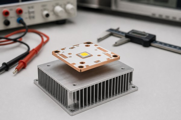
For the heatsink interface, use enough TIM to fill microscopic surface gaps without creating an unnecessarily thick bondline. Board and heatsink flatness determine how evenly that layer is compressed. Fastener placement and torque influence pressure distribution; excessive local force can bend the MCPCB, while insufficient force leaves high-resistance gaps. Electrically conductive TIMs also require clearance and contamination review.
| Interface | Failure Mechanism | Control or Evidence |
| LED-to-pedestal solder | Voids, poor wetting, excessive thickness, or package tilt | Stencil control, reflow record, X-ray, and section evidence |
| MCPCB-to-TIM | Incomplete coverage or trapped debris | Controlled dispense or pad placement and contact-imprint review |
| TIM bondline | Excess thickness, pump-out, or dry regions | Specified material, application amount, and cycling inspection |
| TIM-to-heatsink | Roughness, contamination, or local air gaps | Surface preparation and flatness verification |
| Mounting system | Uneven pressure, board bending, or fastener relaxation | Defined sequence, torque or force control, and post-cycle recheck |
How Should a Finished High-Power LED Module Be Thermally Tested and Validated?
Validate the complete assembled module at worst-case power, ambient temperature, orientation, and realistic airflow. A bare-board material value cannot prove the operating junction temperature. The test must include the actual LED ordering code, solder process, MCPCB, TIM, heatsink, enclosure, mounting method, driver behavior, and cooling condition.
- Define the configuration: Record the LED code, current, electrical input, optical operating mode, board revision, TIM, heatsink, enclosure, orientation, and airflow.
- Select the temperature method: Use the LED manufacturer’s specified junction, case, or solder-point method and document the exact sensor location.
- Control the measurement: Minimize thermocouple heat sinking and attachment error; set emissivity deliberately when using thermography.
- Reach stabilization: Establish a criterion based on the rate of temperature change rather than an arbitrary short test time.
- Test operating limits: Repeat at maximum expected ambient, electrical tolerance, and realistic airflow restriction.
- Compare samples: Include enough assemblies to reveal variation in solder, flatness, TIM application, and mounting.
- Inspect after testing: Check solder alignment, joint condition, TIM coverage, fastener condition, board flatness, and electrical isolation.
Measure the temperature at the reference point defined for the LED’s published thermal resistance. A sensor placed farther away may report a lower temperature and make the calculated junction value appear safer than it is. For clustered LEDs, monitor the central and hottest devices rather than assuming every emitter operates at the average board temperature.
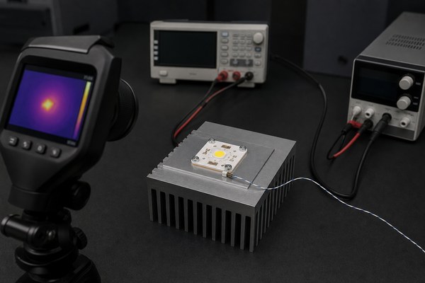
When technology selection remains uncertain, build controlled aluminum-MCPCB and Cu-DTP variants using the same LED, footprint, solder process, TIM, heatsink, mounting, power, ambient, and measurement method. The comparison then isolates the board construction more effectively than unrelated catalog values.
Which Thermal and Manufacturing Problems Commonly Affect Cu-DTP LED Boards?
Troubleshooting should separate local source defects, board-to-heatsink interface problems, and insufficient heat rejection to ambient. The temperature pattern across the LED, board, and heatsink usually indicates where to investigate first. Do not assume that every hot LED proves the MCPCB construction is defective.
| Observed Symptom | Probable Cause | Discriminating Check |
| One LED is hotter than adjacent devices | Local solder void, pad misalignment, LED variation, or current imbalance | Compare current, X-ray evidence, placement, and the local temperature map |
| LED region is hot while the heatsink remains relatively cool | Poor solder transfer, incomplete TIM coverage, excessive bondline, or weak mounting contact | Measure both sides of each interface and inspect the TIM contact imprint |
| All LEDs and the heatsink base are hot | Insufficient heatsink capacity, restricted airflow, or high ambient | Repeat with characterized airflow or a known heatsink under the same electrical load |
| Temperature varies strongly among nominally identical boards | Pedestal tolerance, board flatness, solder, TIM, or mounting variation | Correlate thermal results with dimensional and assembly records |
| Temperature rises after repeated cycling | TIM pump-out, fastener relaxation, joint degradation, or surface movement | Recheck torque, bondline distribution, flatness, and thermal response after cycling |
| Electrical leakage or unexpected continuity appears | Incorrect pad potential, inadequate clearance, conductive contamination, or isolation damage | Perform continuity and insulation checks against the released connection scheme |
Corrective action should follow evidence. For example, changing the heatsink will not repair pedestal misregistration, while tightening fasteners will not solve a solder void under one emitter. Retest the affected interface after each change and preserve the original operating conditions so the result remains comparable.
What Files and Specifications Are Required for a Copper Direct-Thermal-Path MCPCB Quote?
A useful quotation package must define the electrical design, direct-path geometry, mechanical interfaces, assembly state, and acceptance evidence. A board image or generic request for a “copper DTP PCB” does not give the supplier enough information to price tooling, tolerances, inspection, or assembly risk.
- Fabrication data: Submit Gerber or ODB++ files, drill data, board outline, layer identification, and revision control.
- Construction drawing: Define base material and thickness, circuit copper, dielectric regions, surface finish, pedestal geometry, flatness, and critical tolerances.
- LED documentation: Include the exact ordering code, package drawing, recommended land pattern, datasheet, and exposed-pad electrical function.
- Assembly files: Provide the BOM, centroid data, paste data, component orientation, stencil requirements, and approved reflow limits when assembly is requested.
- Mechanical interface: Supply the heatsink drawing, mounting-hole details, TIM choice or target bondline, and fastening method.
- Electrical requirements: State operating current, voltage, circuit topology, isolation requirement, and continuity test points.
- Acceptance plan: Define dimensional inspection, cross-section or X-ray evidence, flatness, electrical test, sample quantity, and thermal validation responsibilities.
- Commercial inputs: State prototype and production quantities, panel constraints if known, delivery location, and required documentation.
Ask the supplier to return a marked DFM review showing the proposed construction, exceptions, controlled dimensions, inspection method, and any assumptions used in the quotation. This turns the quote into a reviewable engineering proposal rather than a price based on an undefined trade name. For additional construction context, compare the proposed design with a dedicated direct thermal path copper PCB manufacturing process.
What Are the Most Common Questions About Copper Direct-Thermal-Path MCPCBs?
Q1: What does MCPCB stand for?
A1: MCPCB stands for metal-core printed circuit board. The metal base spreads heat, while the circuit layer routes power and signals to the LED.
Q2: Do high-power LEDs still need a heatsink with Cu-DTP?
A2: Yes, most high-power LED modules still need a suitable heatsink. Cu-DTP improves heat transfer into the base, but the module must still reject that heat to the environment.
Q3: What heatsink material works best with a Cu-DTP LED module?
A3: Select the heatsink by required thermal resistance, geometry, mass, airflow, weight, corrosion, and cost. Material conductivity alone does not determine the assembled result.
Q4: What are the best thermal interface materials?
A4: The best TIM is the one that meets the required interface resistance and assembly conditions at a controlled bondline. Compare electrical insulation, pump-out resistance, application method, service temperature, and rework needs.
Q5: What is thermal interface material made of?
A5: TIMs may use grease, phase-change compounds, filled elastomer pads, gels, adhesives, or other thermally conductive systems. The approved product must match the module’s electrical, mechanical, and reliability requirements.
Q6: Does copper have better thermal conductivity than aluminum?
A6: Bulk copper generally conducts heat better than bulk aluminum. That fact does not by itself prove that a finished copper board will outperform every aluminum MCPCB because dielectric and interface resistances also matter.
Q7: Why use aluminum instead of copper?
A7: Aluminum may be preferred when its thermal performance is sufficient and lower weight, material cost, or easier machining matters. Select the board from the complete thermal and mechanical requirement.
Q8: What is the maximum allowable LED junction temperature?
A8: Use the maximum junction temperature stated for the exact LED ordering code. Set the normal design target below that absolute limit to preserve margin for ambient, power, material, and assembly variation.
Q9: At what temperature should a high-power LED be soldered?
A9: Follow the LED manufacturer’s qualified reflow profile and exposure limits. Do not select a universal peak temperature without checking the package, solder alloy, board mass, and assembly process.
Q10: Why will solder not wet an LED MCPCB pad?
A10: Poor wetting commonly points to oxidation, contamination, insufficient flux activity, inadequate heating, or an unsuitable surface condition. Inspect the finish and process before increasing temperature or dwell time.
Conclusion
A successful Cu-DTP LED module begins with a thermal budget and ends with validation of the complete assembled heat path. Confirm the LED pad potential, define the copper pedestal and insulation boundaries, calculate realistic resistance allowances, control solder and heatsink interfaces, and test the module at its worst credible operating condition. The result should be judged by measured junction-temperature margin and repeatable manufacturing evidence—not by the board name alone.
If you need a DFM review or quotation for a copper direct-thermal-path MCPCB, email sales@bestpcbs.com with your Gerber or ODB++ data, fabrication drawing, LED datasheet, BOM, quantities, heatsink interface, operating conditions, and required inspection or thermal-test criteria.