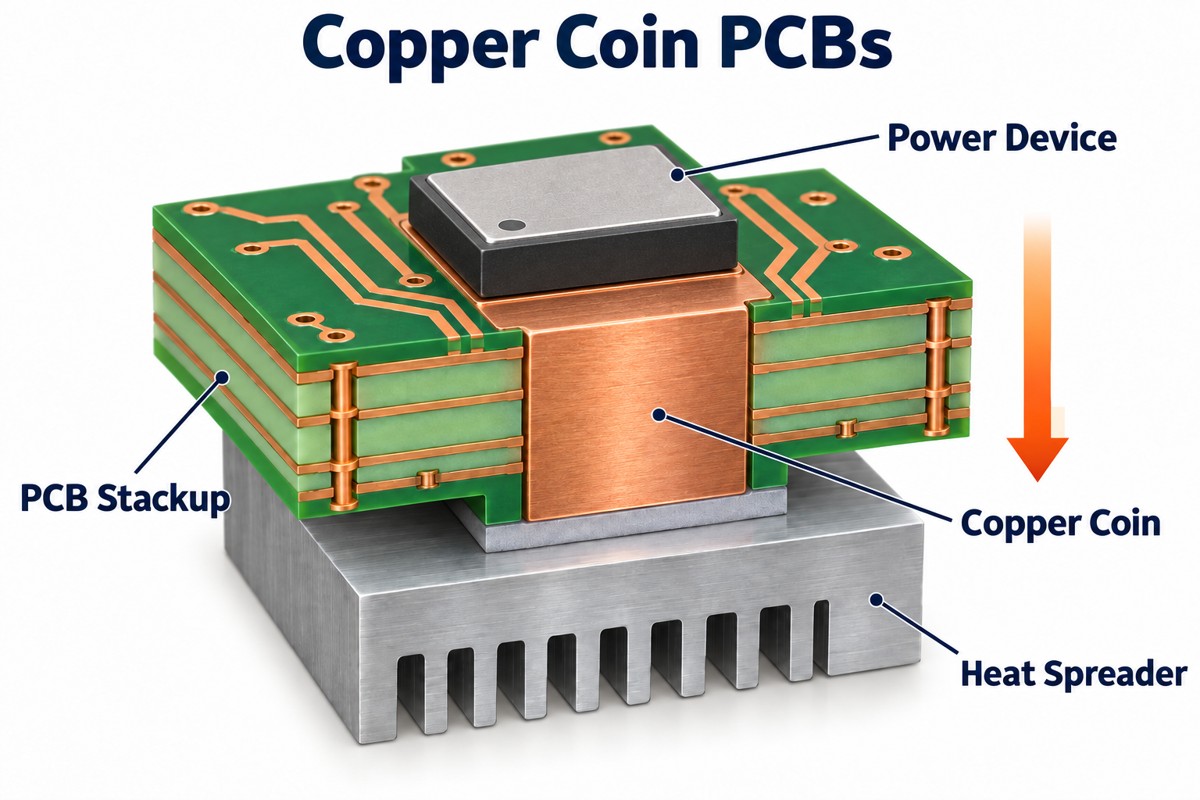
Copper coin PCBs use a solid copper insert to conduct heat through a localized region of a circuit board. They are useful beneath concentrated heat sources such as power transistors and RF amplifiers when the board must connect that hot spot to a heatsink or chassis. Successful cooling depends on more than copper conductivity: coin area, path length, surface height, solder attachment and the heatsink interface all matter. Before fabrication, specify the insert geometry and its relationship to the finished PCB surfaces, then check the complete thermal path under the intended operating conditions.
Key Takeaways
- A copper coin creates a localized conductive path; it is not the same as thicker copper traces or a full metal-core board.
- For a simple through-thickness model, thermal resistance depends on length divided by conductivity and area. The worked example below excludes interfaces and heat spreading.
- A larger coin helps only if heat can enter it and leave it through a suitable attachment and heatsink interface.
- Define X–Y location, coin thickness, surface height, flatness, finish and electrical clearances separately on the fabrication drawing.
- Coin insertion and lamination details depend on the selected construction; agree the process before releasing the stackup.
- Electrical continuity does not verify cooling performance. Dimensional checks, interface inspection and assembly-level thermal validation answer different questions.
- At EBest Circuit, we can review fabrication and PCBA requirements together so the board drawing, component attachment and inspection scope remain aligned.
What Changes When You Add a Copper Coin to a PCB?
A coin replaces part of the local board volume with solid copper, changing the heat path, routing space and mechanical interfaces at that location.
In a through-board construction, heat can travel from the component attachment through the coin to a bottom-side interface. A partial-depth insert leaves other layers above or below it, so those layers remain part of the thermal path. A stepped or T-shaped insert can connect a small device contact area to a wider region, but it also changes the cavity and assembly requirements.
| Structure | Heat-transfer feature | Main design constraint |
| Through-board coin | Solid copper spans the board thickness | Top and bottom contact geometry |
| Partial-depth coin | Copper occupies selected stackup layers | Remaining dielectric and copper layers in the path |
| Stepped or T-shaped coin | Different contact areas at different depths | Shoulder geometry and available routing space |
| Thermal via array | Multiple plated or filled holes conduct heat | Via construction, quantity and spreading area |
| Heavy copper layers | Thicker conductors spread heat in-plane | Etching geometry and layer thickness |
At EBest Circuit, we support PCB fabrication and assembly projects from prototype through production. For a coin-based design, bring us the component attachment drawing and cooling arrangement along with the FR4 PCB stackup. We can review the manufacturing requirements before you lock the mechanical dimensions.
Copper Coin PCB Design: How Should You Size the Insert?
Size the coin from the device’s usable thermal contact area, the allowed temperature rise and the available heat-exit area—not from the package outline alone.
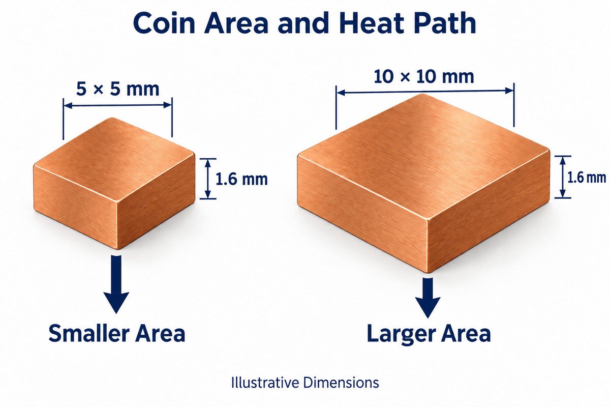
For a first estimate of a uniform solid block, use R = L / (k × A), where R is thermal resistance in K/W, L is heat-path length in meters, k is thermal conductivity in W/(m·K), and A is cross-sectional area in square meters.
The following calculation assumes k = 400 W/(m·K), a rounded illustrative value for high-conductivity copper. It assumes uniform, one-dimensional conduction through a 1.6 mm thickness. These are example dimensions, not a statement of our manufacturing limits.
| Coin cross section | Calculated coin resistance | Rise across coin at 10 W |
| 5 × 5 mm | 0.16 K/W | 1.6 K |
| 10 × 10 mm | 0.04 K/W | 0.4 K |
Doubling both side lengths quadruples the area and reduces this calculated resistance to one quarter. It does not mean the device junction temperature falls by the same ratio: the package, solder, spreading resistance, interface material and heatsink are absent from this calculation.
- Start with the actual exposed pad or flange drawing, including its electrical connection.
- Check whether a larger footprint removes space needed for vias, planes or mounting features.
- Use the real copper grade and temperature-dependent properties in detailed modeling.
- Evaluate a stepped insert when the device and heatsink contact areas differ substantially.
Why Can the Interface Matter More Than the Coin?
A low-conductivity or poorly contacting interface can contribute more thermal resistance than the solid copper beneath it.
For example, a uniform 0.10 mm interface layer with an assumed conductivity of 3 W/(m·K) over 5 × 5 mm has a calculated bulk resistance of about 1.33 K/W. That is much larger than the 0.16 K/W copper-block example. Actual interface performance also includes contact resistance and depends on compression and surface condition; use the interface supplier’s data for the intended assembly.
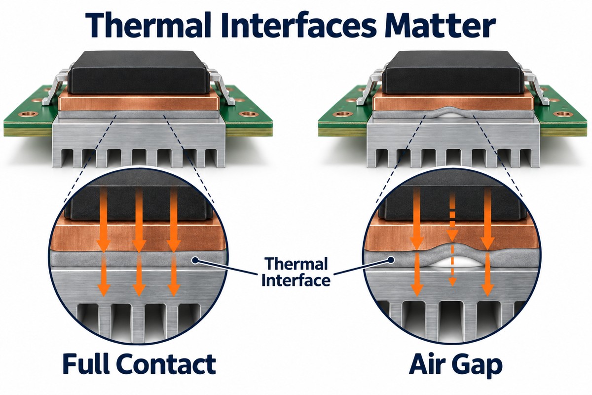
Control the surfaces at both ends of the coin:
- Device side: solderable finish, pad geometry, solder volume and attachment voiding.
- Heatsink side: interface material, final gap, mounting pressure and surface flatness.
- Mechanical assembly: fastener location and support so tightening does not bend the board away from the coin.
Our PCB heatsink design guide covers the surrounding cooling arrangement. Here, the critical boundary is the actual contact between the coin and that arrangement.
Which Tolerances Belong on the Fabrication Drawing?
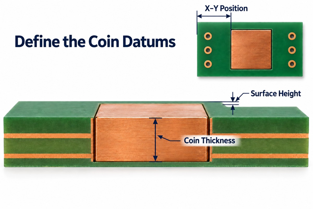
Specify coin location, outline, thickness, top and bottom surface offsets, and contact-face flatness against explicit datums.
“Flush copper coin” is incomplete unless the drawing identifies the reference surface and acceptable deviation. The bare laminate surface, finished copper land and solder-mask surface are different height references. Also state whether dimensions apply before or after plating and final finishing.
| Drawing field | Definition to include |
| X–Y position | Coin center or edge relative to board datums |
| Outline and corner radius | Finished insert geometry and orientation |
| Coin thickness | Finished thickness or stepped-section dimensions |
| Surface height | Allowed recess or protrusion relative to named PCB surfaces |
| Flatness | Permitted variation across each contact face |
| Finish | Finish type and applicable contact surfaces |
| Electrical separation | Clearances to unrelated conductors and any required insulation |
Consider a simple tolerance stack: if a nominal 1.60 mm board and a separate nominal 1.60 mm coin each have an independent ±0.10 mm thickness allowance, their total thickness mismatch can reach 0.20 mm. Matching nominal dimensions therefore does not ensure two flush faces. This is an arithmetic example, not a recommended tolerance; the insertion datum and finishing process determine how that mismatch appears.
Agree finished-part requirements with the fabricator first. Cavity allowances, insertion fit and process compensation should then follow the qualified construction rather than an arbitrary universal gap.
Copper Coin PCB Process: What Must Be Agreed Before Production?
The process must define how the insert is retained, when it enters the stackup, and how its final contact surfaces are produced.
Press-fit, bonded and laminated-in constructions do not use one interchangeable manufacturing sequence. A practical process review covers these stages, with the order adjusted to the selected construction:
- Review the stackup and coin drawing: confirm routing restrictions, electrical connections, cavity geometry and inspection datums.
- Prepare the coin and cavity: machine the required shape, control burrs and clean the joining surfaces.
- Integrate the insert: use the agreed retention, bonding or lamination route and control registration.
- Complete the board: carry out the applicable drilling, metallization, circuitry and finishing operations.
- Verify the finished interfaces: measure height and geometry, inspect the relevant boundaries, and perform the specified electrical tests.
Copper coin PCB technology adds a metal-to-board interface that ordinary stackup notes may not describe. Put the selected structure in a cross-sectional drawing so purchasing, fabrication and assembly work from the same definition.
How Do You Prevent Electrical and Assembly Problems?
Assign the coin an electrical function, maintain the required conductor separation, and qualify the component’s soldering process on the actual thermal structure.
Copper conducts electricity as well as heat. A transistor tab or exposed pad may be connected to a switching node rather than ground. Connecting its coin directly to a grounded heatsink without the necessary isolation can create an electrical fault.
- Identify the coin’s net, or state that it must remain isolated.
- Review internal-plane clearances as well as visible surface spacing.
- If insulation is needed, specify the isolation arrangement and include its thermal resistance in the model.
- Keep solder-mask openings and solderable surfaces consistent with the component attachment drawing.
- Measure the reflow profile near the large copper mass; do not assume a profile qualified on a standard board transfers unchanged.
Through our PCB assembly service, we can review the BOM, placement data and assembly drawing together with the fabrication package. Define attachment acceptance criteria before the first build, particularly for joints hidden beneath a power package.
Which Inspections Verify Copper Coin PCBs?
Use dimensional measurement for geometry, cross sections for the relevant internal interfaces, and a powered thermal test for the assembled cooling path.
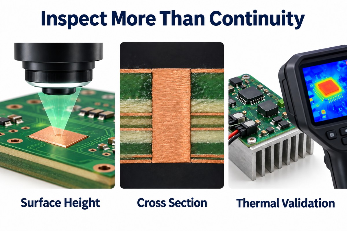
- Dimensional inspection: verify coin location, face height, flatness and finished board dimensions against the drawing.
- Cross-sectional inspection: examine the specified coin boundary, surrounding laminate and any required metallized connection on a suitable sample or coupon.
- Electrical testing: verify required connections and isolation; this does not establish thermal resistance.
- Assembly inspection: use appropriate X-ray inspection for hidden solder attachment where applicable, with agreed voiding criteria.
- Thermal validation: test the assembled device, interface and heatsink at defined power, airflow and ambient conditions.
For thermal-camera measurements, account for the low and variable emissivity of shiny metal. Use a suitable calibrated measurement method rather than comparing uncorrected apparent temperatures. Record the sensor location, operating load, interface material and mounting conditions so later builds can be compared.
When Are Thermal Vias or Heavy Copper a Better Choice?
Thermal vias or heavier copper are preferable when they meet the temperature target without the added cavity, insert and interface controls of a coin.
A via array can be appropriate when the heat source is moderate and the available board area supports enough vertical and lateral conduction. Heavy copper PCBs are useful when current carrying and in-plane heat spreading are central requirements. Neither approach automatically matches a solid coin’s localized through-board path.
Compare alternatives with the same device losses, mounting arrangement and temperature limit. A coin is most compelling when a concentrated hot spot and a nearby heat-exit surface justify the extra fabrication effort. Increasing copper volume without improving the exit path may add cost without solving the bottleneck.
What Should a Copper Coin PCB Manufacturer Confirm in a Quote?
The quote should identify the approved coin construction, finished tolerances, inspection scope and any tooling or qualification work required.
Ask for confirmation of these items rather than a generic claim of “excellent heat dissipation”:
- Coin material, geometry, finish and retention method.
- Finished board thickness and coin-to-board surface requirements.
- Quantity of inserts, panel arrangement and machining complexity.
- Dimensional reports, cross-section sampling and electrical test coverage.
- Whether component attachment and thermal validation are included or supplied separately.
Cost is affected by insert shape, cavity preparation, registration, surface finishing and inspection—not just copper weight. Keep tolerances tight where they control solder attachment or heatsink contact; avoid applying the same tight limit to unrelated features.
FAQ About Copper Coin PCBs
Does a copper coin have to be round?
No. A coin is a solid copper insert and may be rectangular, stepped or another manufacturable shape. Its geometry follows the device contact area, available routing space and cooling interface.
Is a thicker coin always better for cooling?
No. For a fixed area and one-dimensional through-thickness conduction, a longer path increases resistance. A different thickness may support a particular mechanical structure or heat-spreading arrangement, but it is not automatically a thermal improvement.
Can a buried coin replace a through-board coin?
Not without checking the remaining layers in the heat path. A buried copper coin PCB can retain routing or laminate above the insert, but those layers change how heat reaches the coin and leaves it.
Can you calculate junction temperature from copper conductivity alone?
No. Junction temperature depends on device power loss and the complete thermal network, including the package, attachment, coin, interfaces and cooling environment. Conductivity describes a material, not the assembled system’s thermal resistance.
Does every copper coin need a plated connection to PCB traces?
No. Some designs require an electrical connection; others require isolation. The drawing must specify that intent, and the chosen fabrication route must support it. Do not infer the connection merely from the presence of a metal insert.
How Can EBest Circuit Help Review Your Copper Coin PCB?
We can review your board fabrication and PCBA requirements together, starting with the coin drawing, stackup and component attachment details.
Send the Gerber or ODB++ data, dimensioned coin cross section, required quantities and heatsink interface information to sales@bestpcbs.com. For assembled boards, include the BOM, placement file and inspection requirements. We will clarify the construction, applicable tolerances and quotation scope with you before production.