





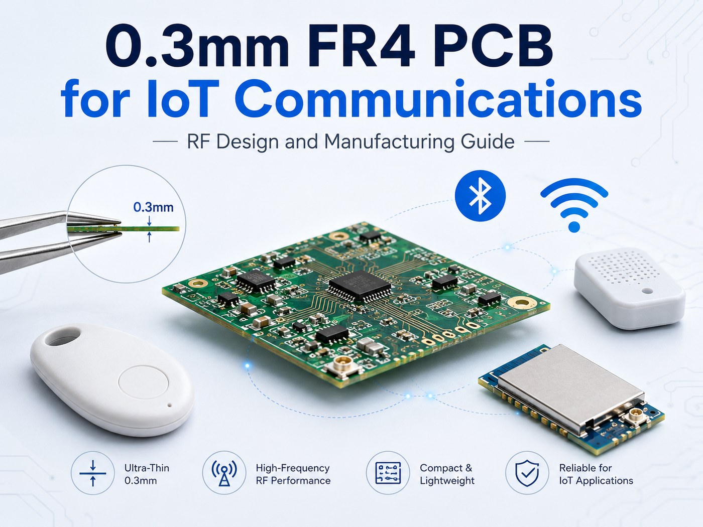
Compact IoT products often need a thinner circuit board without moving to a flexible PCB. A 0.3mm FR4 PCB for IoT communications can reduce the electronic stack height while keeping the familiar material system, component mounting, and assembly methods of a rigid board.
That makes it useful for Bluetooth devices, Wi-Fi modules, wireless sensors, trackers, smart tags, and other products where internal space is tight. The trade-off is that a thinner FR4 construction changes board stiffness, RF geometry, manufacturing handling, and SMT support. These points should be considered before the stack-up is finalized.
What Is a 0.3mm FR4 PCB?
A 0.3mm FR4 PCB is an ultra-thin rigid printed circuit board with a finished thickness of approximately 0.3mm, or about 11.8 mil. It uses glass-reinforced epoxy laminate as the insulating and structural substrate, just like conventional FR4 boards, but with a much thinner overall construction.
In most PCB specifications, 0.3mm refers to the finished board thickness, including the dielectric structure and copper layers. It should not be confused with a 0.3mm FR4 core, which would result in a thicker finished PCB after copper, plating, and surface coatings are added.
Compared with common 0.8mm, 1.0mm, or 1.6mm rigid boards, a 0.3mm board has much lower stiffness and is generally considered an ultra thin FR4 PCB. It is still a rigid-board construction rather than an FPC.
Why Use a 0.3mm Ultra Thin FR4 PCB for IoT Communications?
The main reason is to reduce the PCB’s contribution to overall product thickness. In compact IoT hardware, even a fraction of a millimeter can affect battery clearance, antenna placement, housing design, or the final device profile.
Typical applications include:
- Bluetooth Low Energy sensor nodes;
- Wi-Fi communication modules;
- smart tags and asset trackers;
- sub-GHz wireless sensors;
- compact access-control devices;
- lightweight handheld electronics;
- thin wearable products where the PCB remains fixed in position.
A 0.3mm board is most useful when enclosure height is genuinely constrained. If product thickness is already determined by a tall connector, display, or battery, reducing the PCB from 0.8mm or 1.0mm to 0.3mm may provide little practical benefit.
For many low-power IoT products, the attraction is therefore mechanical rather than electrical: the board stays rigid enough for conventional component mounting while occupying much less vertical space.
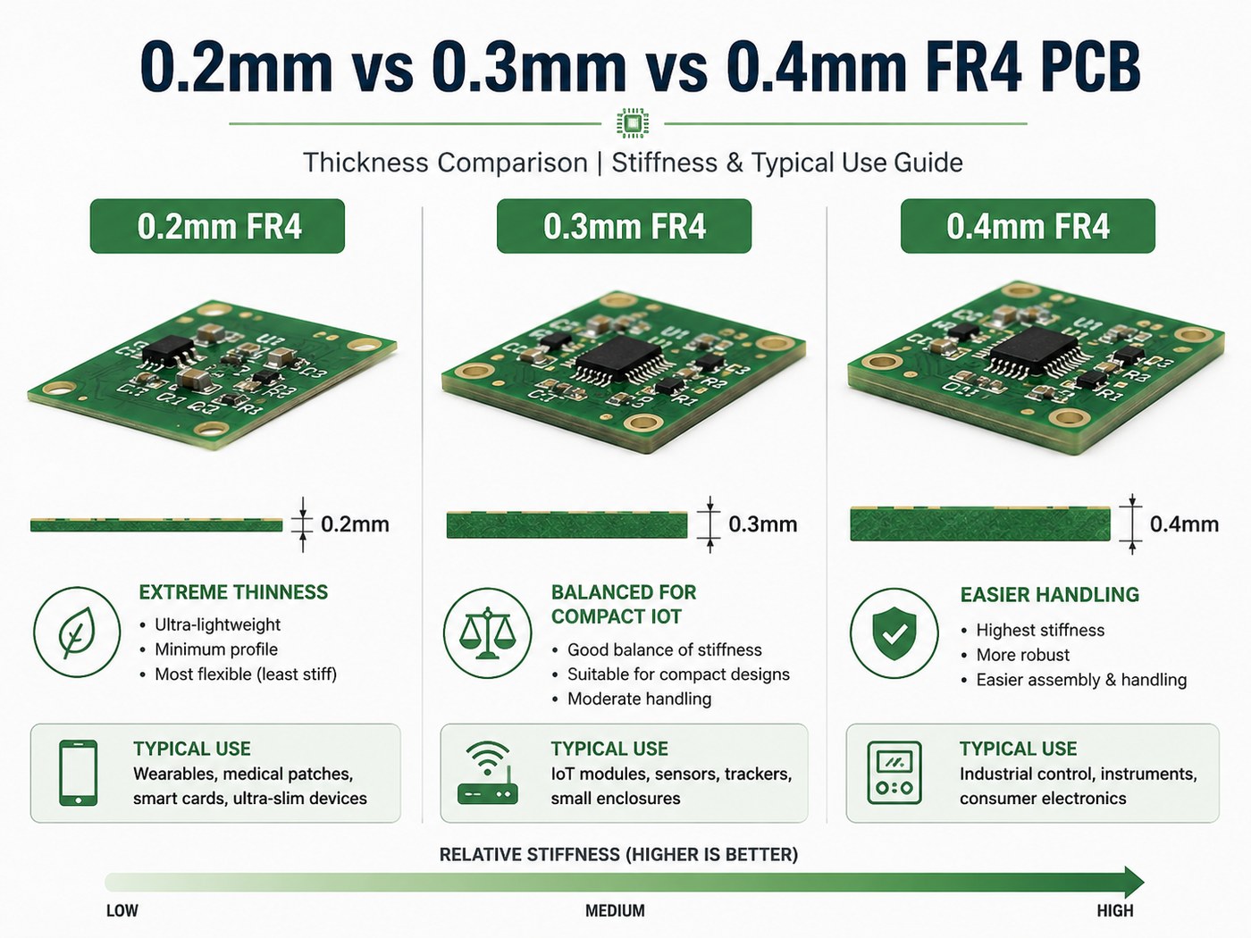
0.2mm vs 0.3mm vs 0.4mm FR4 PCB: Which Thickness Is Better?
The right thickness is usually the thinnest construction that solves the mechanical problem without adding unnecessary fabrication and assembly difficulty.
For a broader baseline, compare these options with the standard PCB thickness used in conventional rigid boards.
| Finished Thickness | Mechanical Behavior | Manufacturing / Assembly | Typical Use |
|---|---|---|---|
| 0.2mm | Very low stiffness | Requires careful support and handling | Severe z-height restrictions |
| 0.3mm | Thin with moderate rigidity | Practical with suitable panel support | Compact IoT modules and sensors |
| 0.4mm | More rigid | Easier to process and assemble | Thin electronics with slightly more clearance |
| 0.8–1.0mm | Conventional rigid behavior | Relatively straightforward | Moderate thickness constraints |
| 1.6mm | High rigidity | Standard PCB construction | Products without tight z-height limits |
For many IoT products, 0.3mm is a useful middle ground between extreme thinness and manufacturing robustness. Going to 0.2mm or even 0.1mm should be driven by a real packaging requirement, because board dimensions, copper weight, layer count, and panel design all become more influential as stiffness decreases.
How Does 0.3mm FR4 Thickness Affect RF and Signal Performance?
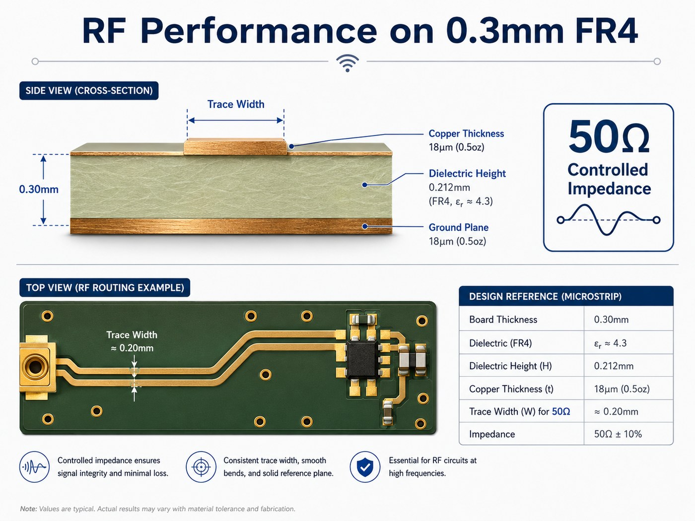
PCB thickness changes the spacing between signal traces and their reference plane. That spacing is one of the main variables used to calculate characteristic impedance.
A 50Ω RF trace designed for a 1.0mm or 1.6mm PCB should therefore not be copied directly onto a 0.3mm board. The required trace geometry must be recalculated using the actual stack-up.
The main variables are:
- dielectric height;
- trace width;
- copper thickness;
- dielectric constant;
- reference-plane location;
- solder mask, when included in the impedance model.
With a smaller dielectric spacing, a 50Ω trace may need to be narrower. This can affect RF IC fan-out, connector launches, spacing to nearby copper, and manufacturable line-width tolerance.
The same principle applies to differential signals. If an IoT board also carries USB, Ethernet, high-speed memory, or other controlled-impedance interfaces, their geometry should be calculated from the final stack-up rather than scaled from a thicker reference design.
What FR4 Dielectric Constant Should You Use for IoT PCB Design?
There is no single dielectric constant that represents every FR4 laminate. The familiar value of 4.4 is useful as a rough reference, but it should not automatically be used for final RF calculations.
Actual Dk varies with factors such as:
- laminate family;
- glass style;
- resin content;
- construction;
- test frequency.
For early feasibility work, a nominal FR4 value is usually enough to estimate trace geometry. For final RF or impedance design, use the laminate manufacturer’s design-relevant Dk whenever that data is available.
It is also important to separate Dk from Df. Dk influences impedance and electrical wavelength, while Df relates to dielectric loss. For a short RF feed in a compact Bluetooth or Wi-Fi device, ordinary FR4 may be adequate. Longer RF paths or stricter loss budgets may require tighter control of both values.
If electrical performance depends on a specific Dk or Df, the fabrication specification should name the laminate or define an acceptable material range instead of stating only “FR4.”
Can a 0.3mm FR4 PCB Support Controlled Impedance?
Yes. A 0.3mm FR4 PCB can support controlled impedance as long as the stack-up produces trace dimensions that the fabricator can manufacture consistently.
A practical controlled impedance PCB design must use the approved production stack-up rather than nominal board thickness alone.
For impedance-controlled nets, define:
- target impedance, such as 50Ω single-ended;
- required tolerance;
- signal layer;
- reference plane;
- copper thickness;
- dielectric construction;
- solder-mask condition;
- coupon or TDR requirements, if needed.
On a very thin stack-up, the calculated trace can become narrow. If the geometry approaches the manufacturer’s process limit, the better solution is usually to adjust the construction rather than force an unnecessarily difficult trace width.
Possible adjustments include changing dielectric spacing, copper weight, layer arrangement, or transmission-line structure. These decisions are much easier to make before routing is finalized.
How Should PCB Antennas Be Designed on 0.3mm FR4?
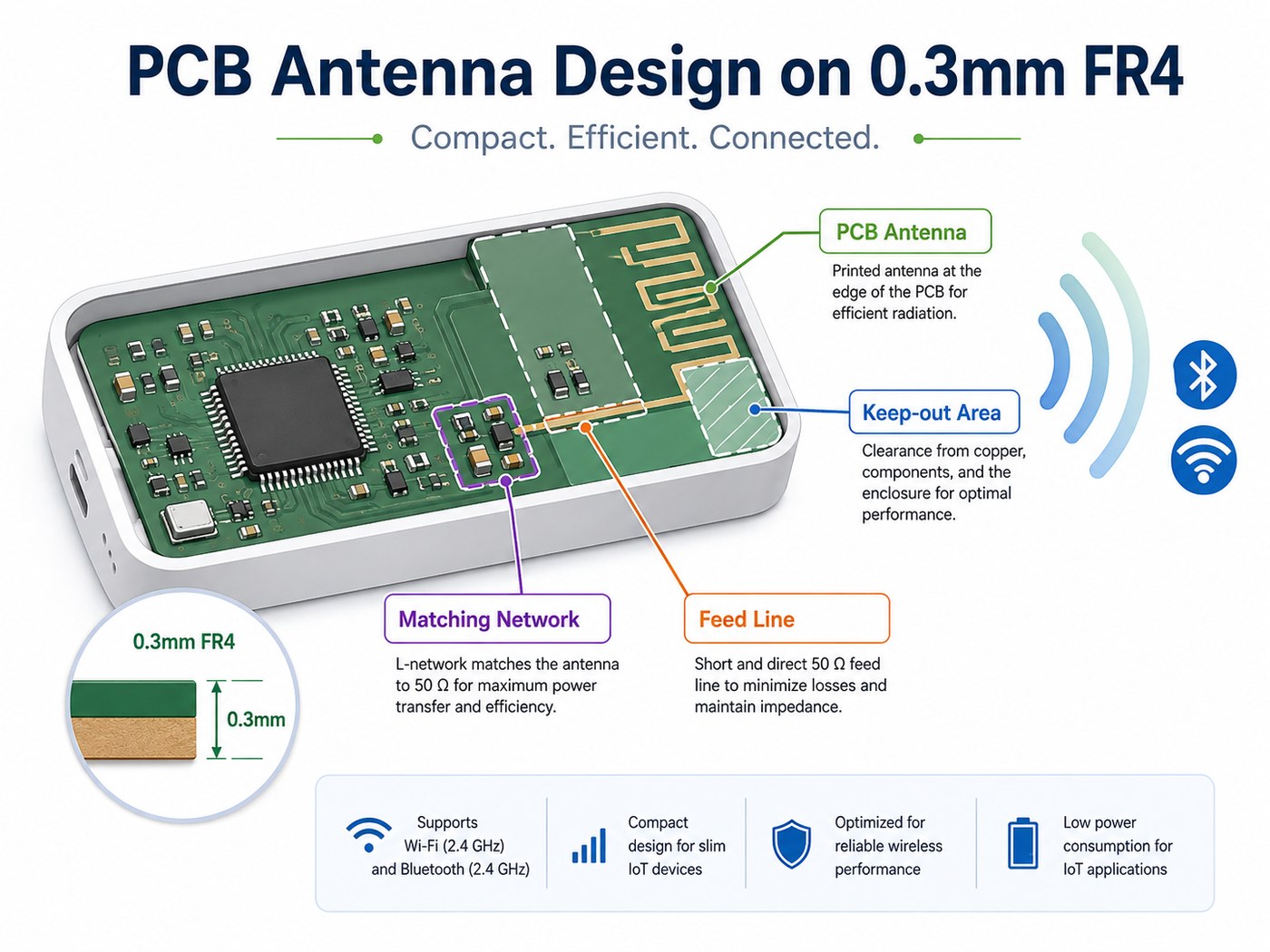
A PCB antenna must be designed around the actual substrate and board geometry. Changing from a thicker reference PCB to 0.3mm FR4 can alter antenna impedance and resonance, even if the copper outline remains unchanged.
This section works as a compact PCB antenna design guide for thin rigid IoT boards, but final tuning must still be completed in the real enclosure.
Several layout details deserve particular attention:
- Antenna placement: keep the antenna near the intended board edge and preserve its keep-out region.
- Ground structure: ground-plane dimensions and nearby copper can influence antenna behavior.
- Feed line: calculate the feed using the actual 0.3mm stack-up.
- Matching network: leave room for the recommended tuning components.
- Nearby hardware: batteries, shielding, displays, cables, metal fasteners, and the enclosure can shift antenna performance.
For Bluetooth, Wi-Fi, and similar IoT products, the antenna should be evaluated after it is installed in the final mechanical environment. A PCB antenna that performs well in free space can behave differently once the battery and enclosure are in place.
What Stack-Up and Copper Thickness Work for a 0.3mm FR4 PCB?
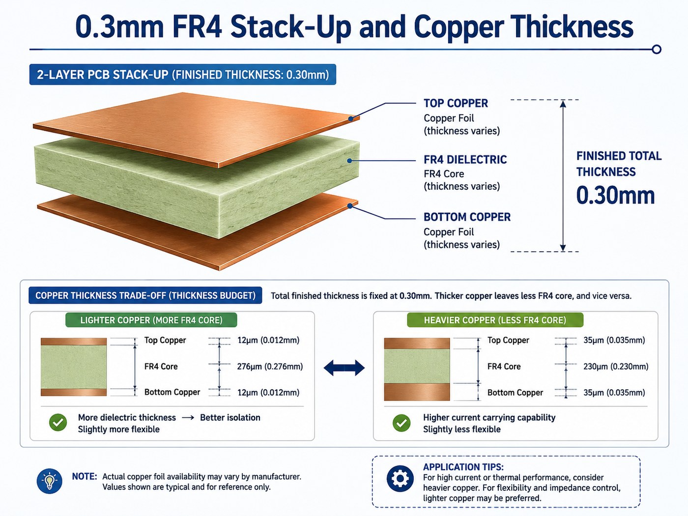
A 0.3mm finished thickness leaves limited space for dielectric material, copper, plating, and solder mask, so the stack-up has to be planned more carefully than on a conventional board.
The FR4 PCB copper thickness must be included in the total 0.30mm finished-thickness budget.
The construction is mainly influenced by:
- layer count;
- copper weight;
- required dielectric spacing;
- via structure;
- impedance requirements;
- finished-thickness tolerance.
A two-layer 0.3mm PCB is generally easier to implement because the material structure is relatively simple. Multilayer versions can also be produced, but the available thickness must be divided among multiple cores, prepregs, and copper layers.
Copper weight should match the electrical need rather than defaulting to a heavier specification. For many low-power IoT circuits, lighter copper gives more freedom for fine routing and controlled-impedance geometry. Heavier copper uses more of the total thickness budget and can make fine-line etching more difficult.
If the requirement is 0.30mm finished thickness, state that directly. Do not specify a 0.3mm FR4 core unless the core itself is the intended requirement.
What Manufacturing Challenges Come With an Ultra Thin FR4 PCB?
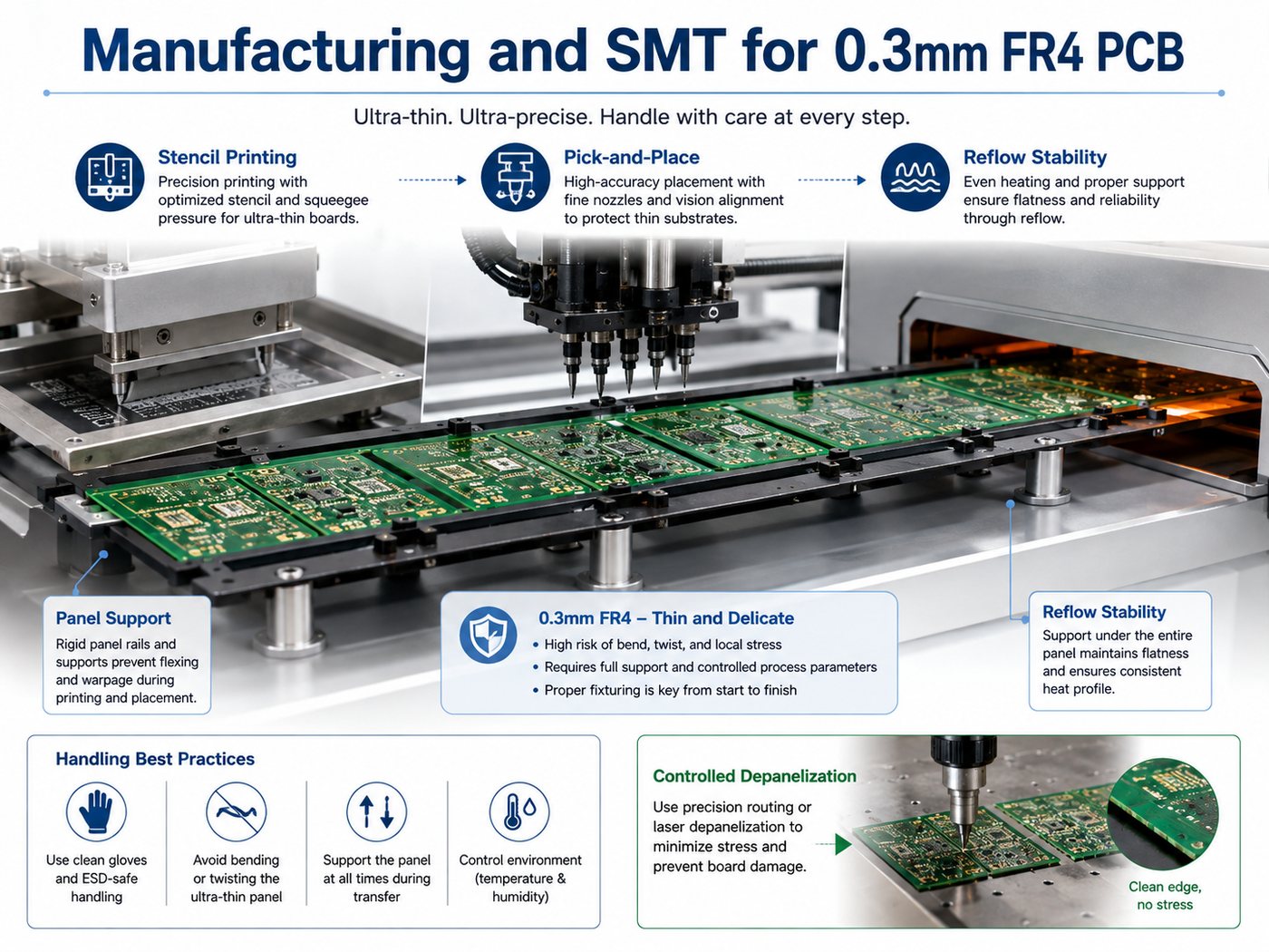
The main fabrication issue is reduced panel stiffness. Thin FR4 can move, bow, or distort more easily during processing, particularly when the board outline is large.
Manufacturing control usually needs more attention in several areas:
- Panel handling: thin panels require better support during transfer and processing.
- Registration: dimensional movement can affect layer-to-layer alignment on dense designs.
- Drilling and routing: stable fixturing helps prevent board movement.
- Solder mask: coating and curing should maintain alignment and flatness.
- Depanelization: excessive bending can damage thin boards or assembled components.
- Final inspection: warpage and dimensional stability need closer attention.
Board size is important here. A small 0.3mm IoT module is much easier to handle than a large 0.3mm panelized circuit with the same nominal thickness.
For this reason, manufacturing feasibility should be reviewed using the actual board outline, layer structure, copper weight, feature sizes, and panel design rather than thickness alone.
How Does 0.3mm PCB Thickness Affect SMT Assembly?
A 0.3mm PCB needs more mechanical support during assembly because it can deflect under stencil pressure, conveyor handling, and thermal stress.
The main assembly considerations are:
- stable panelization;
- adequate underside support during solder paste printing;
- reliable conveyor transport;
- reflow warpage;
- component weight and distribution;
- controlled depanelization.
Lightweight IoT assemblies are generally easier to process. Boards populated mainly with QFN, LGA, small sensors, and passive components place less mechanical stress on the PCB than designs carrying large connectors, transformers, inductors, or heavy shielding cans.
Prototype assembly should ideally use the intended production panel rather than loose individual boards. This exposes printing, transport, reflow, and depanelization issues before the design moves into volume production.
0.3mm FR4 PCB vs Flex PCB vs RF Laminate: Which Should You Choose?
The choice depends on the main requirement. Thin FR4 suits a low-profile rigid circuit, flex PCB suits a circuit that must bend, and low-loss RF laminate suits designs where dielectric loss or RF consistency is more important than standard FR4 economics.
| Requirement | 0.3mm FR4 PCB | Flex PCB | Low-Loss RF Laminate |
|---|---|---|---|
| Thin profile | Very good | Excellent | Depends on construction |
| Repeated bending | Poor choice | Excellent | Generally not the purpose |
| Rigid component platform | Good | Requires support consideration | Good |
| Conventional SMT | Familiar | More support often needed | Similar to rigid PCB |
| Material cost | Usually economical | Usually higher | Usually higher |
| RF consistency | Adequate for many IoT designs | Material-dependent | Typically better controlled |
| Compact BLE/Wi-Fi product | Strong candidate | Useful if folding is needed | Often unnecessary |
| Dynamic wearable | Limited | Strong candidate | Limited |
| Demanding RF transmission path | Evaluate carefully | Specialized | Strong candidate |
A Bluetooth or Wi-Fi design does not automatically require a premium RF laminate. Short RF feeds and properly tuned antennas can work well on suitable FR4. Likewise, thin FR4 should not be used as a substitute for FPC when repeated bending is part of normal operation.
How Should You Specify a 0.3mm FR4 PCB for Manufacturing?
A clear fabrication package is especially important for ultra-thin boards because thickness, copper, stack-up, and impedance requirements interact with each other.
Define the FR4 PCB thickness tolerance on the fabrication drawing when enclosure fit, connector alignment, or RF geometry depends on it.
For quotation and DFM review, provide:
- finished board thickness and tolerance;
- layer count;
- board dimensions;
- copper weight;
- preferred FR4 material, if required;
- Dk/Df requirements, where relevant;
- stack-up, if already approved;
- controlled-impedance targets and tolerance;
- minimum line/space;
- hole and via requirements;
- surface finish;
- Gerber or ODB++ files;
- NC drill files;
- fabrication drawing;
- panelization requirements;
- assembly files, if PCBA is required;
- RF-critical dimensions and antenna keep-out areas.
If the stack-up has not been finalized, it is usually better to specify the electrical requirement and allow the fabricator to propose a manufacturable construction. For example:
Finished thickness 0.30mm, 2-layer FR4, 50Ω RF feed, final trace geometry to be confirmed against the production stack-up.
For projects reviewed by EBest Circuit, sending the complete fabrication package together with RF, impedance, and assembly requirements helps engineering distinguish fixed specifications from items that can still be adjusted before prototyping.
FAQs About 0.3mm Ultra Thin FR4 PCB
Is a 0.3mm FR4 PCB flexible?
It can bend more easily than a normal 1.0mm or 1.6mm rigid PCB, but it should not be treated as a flex circuit. Use it where a thin rigid board remains substantially flat in service. If the circuit must repeatedly bend or fold, use an FPC construction designed for that mechanical duty.
How thin can an FR4 PCB be?
FR4 PCBs can be manufactured below 0.3mm, but there is no universal “thinnest FR4 PCB” specification. The achievable thickness depends on board size, layer count, copper, dielectric construction, feature density, panel support, and the manufacturer’s process. Very thin values such as 0.1mm should be confirmed against the actual design rather than treated as standard capability.
Can a 0.3mm FR4 PCB have multiple layers?
Yes, but the thinner the finished board becomes, the less thickness is available for cores, prepregs, copper, and plating. Two-layer construction is relatively straightforward to evaluate. A 0.3mm multilayer PCB should be designed around a manufacturer-approved stack-up before routing and impedance geometry are finalized.
Can a 0.3mm FR4 PCB be used for Bluetooth or Wi-Fi antennas?
Yes. FR4 PCB antennas are used in many 2.4GHz applications, but antenna geometry should be designed or retuned for the actual board material, thickness, ground structure, enclosure, and feed line. Reference-antenna dimensions from another PCB thickness should not be copied blindly.
What dielectric constant should I use for a 0.3mm FR4 PCB?
Use the Dk associated with the actual laminate construction and relevant frequency whenever impedance or antenna performance is important. Do not assume every FR4 material has a dielectric constant of exactly 4.4. Published laminate data shows that Dk can vary with resin content, glass construction, and frequency.
How Can EBest Circuit Support Your 0.3mm FR4 PCB Project?
At EBest Circuit, we support ultra-thin FR4 PCB fabrication, controlled-impedance review, and PCB assembly for compact IoT products. We review the finished thickness together with the stack-up, copper weight, board dimensions, RF requirements, panel design, and assembly conditions.0.3mm FR4 PCB is a practical choice when an IoT product needs a thin rigid circuit without the bending requirements of FPC or the added cost of a specialized RF laminate. The key is to treat the 0.3mm thickness as part of the electrical and manufacturing design, not just as a mechanical specification.
Send us your Gerber or ODB++ files, fabrication drawing, target thickness and tolerance, stack-up, impedance targets, BOM, assembly files, and quantity at sales@bestpcbs.com.







