A camera PCB module is the electronic foundation behind many imaging products. It connects the image sensor, lens module, connector, power circuit, signal path, and control components into a compact assembly that captures, processes, and transmits image data. For engineers, it is not just a small circuit board. It is a high-density and signal-sensitive module where layout, impedance, FPC connection, soldering quality, cleanliness, and testing can directly affect image stability and product reliability.
EBest Circuit supports camera PCB module projects from PCB fabrication to component sourcing, SMT assembly, DFM review, testing, and small-batch production. With over 20 years of PCB and PCBA experience, our engineering team helps customers review manufacturing risks before production and keep key requirements controlled through assembly and delivery. If you are developing a PCB camera module, or camera PCBA project, send your files or questions to sales@bestpcbs.com. We will help you move from engineering files to a reliable build.
What Is a Camera PCB Module?
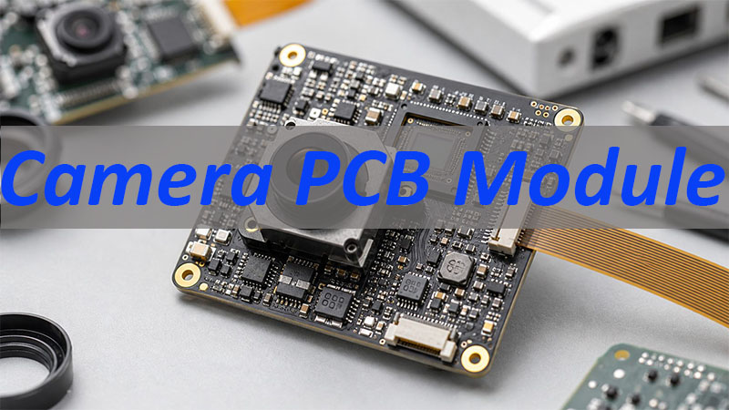
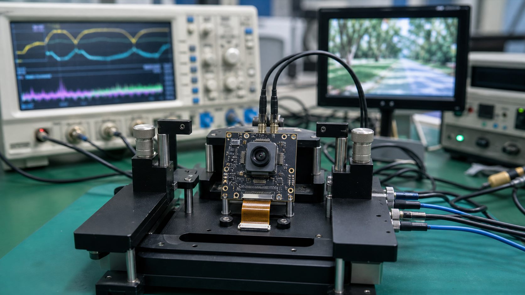
A camera PCB module is a printed circuit board assembly used to support and connect camera-related components. It usually includes an image sensor, lens interface, connector, passive components, power management circuit, and signal transmission path. Depending on the application, it may also include FPC, shielding, LEDs, microphones, memory, processor, or interface ICs.
In simple terms, the camera PCB module acts as the electrical and mechanical platform for the camera. It provides:
- Signal routing between the image sensor and host device
- Stable power supply for the sensor and control circuit
- Connector support for FPC, board-to-board, USB, MIPI, or other interfaces
- Mechanical support for lens and sensor alignment
- EMI control and grounding paths
- Assembly pads for SMT components
- Test points for inspection and validation
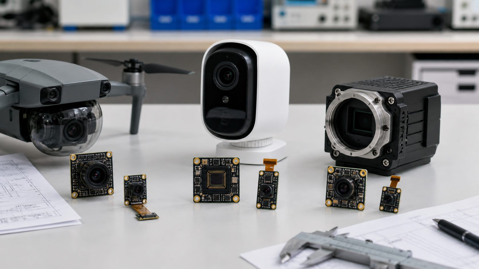
Camera PCB modules are used in many products, including security cameras, IP cameras, drones, smart home devices, medical imaging equipment, industrial vision systems, automotive cameras, barcode scanners, wearable devices, and embedded vision products.
Because the board often works with high-speed image signals and compact mechanical structures, the PCB must be manufactured and assembled with tighter control than many general-purpose circuit boards.
PCB Camera Module vs Camera Module PCB
The terms PCB camera module and camera module PCB are often used in similar ways, but they can emphasize different parts of the product.
| Term | Meaning |
|---|---|
| Camera PCB module | Complete camera-related PCBA or module |
| PCB camera module | Camera module built on a PCB platform |
| Camera module PCB | Bare or assembled PCB inside the module |
| Camera module PCB assembly | PCB with SMT parts, connector, and sensor area |
For purchasing and engineering communication, it is helpful to clarify whether the project requires only a bare camera module PCB, a PCB with SMT assembly, or a complete camera PCB module with components, testing, and packaging.
For example, one customer may only need a small rigid PCB for a CMOS sensor. Another may need flexible PCB for camera module connection. A third customer may need turnkey support, including PCB fabrication, component sourcing, SMT assembly, lens-related assembly support, functional testing, and delivery control.
That is why early communication matters. If the supplier only understands bare PCB fabrication, important PCBA risks may be missed. If the supplier understands both PCB manufacturing and assembly, the team can review the project from a more practical production point of view.
Camera Module PCB Structure and Key Components
A camera module PCB is usually compact but component-dense. Its exact structure depends on product size, resolution, interface, sensor type, and mechanical housing. However, most camera module PCB projects include several common elements.
| Part | Role |
|---|---|
| Image sensor area | Captures light signals |
| Lens module interface | Supports lens alignment |
| Connector | Links to the host board |
| Power circuit | Supplies stable voltage |
| Passive components | Filters noise and stabilizes signals |
| Signal routing | Carries image, clock, and control data |
| Grounding and shielding | Reduces EMI risk |
| Test points | Supports inspection and testing |
The camera lens module PCB area requires special attention. The relationship between the lens, sensor, board flatness, and mechanical tolerance can directly affect image quality. Even when the electrical design is correct, poor mechanical fit or assembly deviation can lead to focus issues, unstable images, or poor production yield.
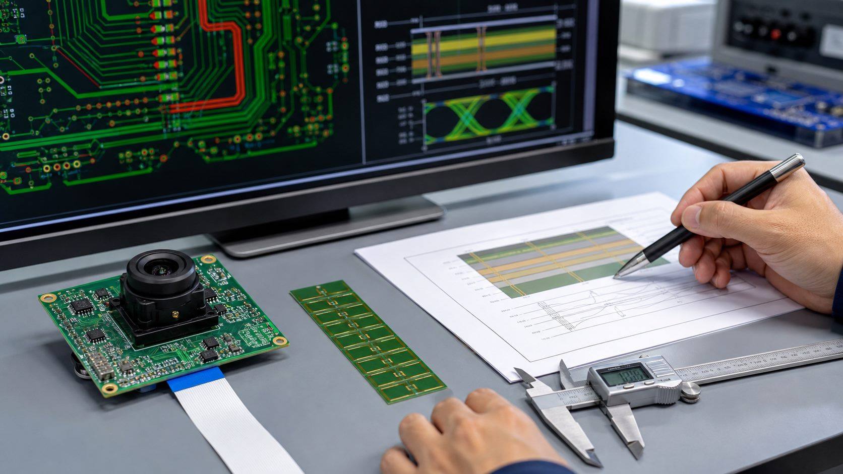
For high-speed interfaces, routing length, impedance, grounding, return path, via placement, and connector selection become more important. A camera module PCB may look small, but the layout and manufacturing requirements can be more demanding than a larger low-speed control board.
Flexible PCB for Camera Module Applications
Flexible PCB for camera module projects is common when the camera needs to fit into a compact, moving, or space-limited product. FPC allows the camera module to connect with the main board while saving space and improving mechanical flexibility.
Flexible PCB for camera modules is often used in:
- Mobile devices
- Drones
- Smart cameras
- Medical handheld devices
- Wearable electronics
- Automotive camera systems
- Display-integrated camera products
- Compact embedded vision devices
Compared with rigid PCB, flexible PCB requires different design and manufacturing considerations. Bend radius, copper type, coverlay openings, stiffener design, connector reinforcement, adhesive selection, and dynamic bending requirements should be reviewed before production.
For engineers, one common mistake is treating FPC like a thin rigid PCB. That can create risks in bending, assembly, connector reliability, and long-term operation. If the project uses a flex PCB camera module, the manufacturer should check both electrical requirements and mechanical usage conditions.
In many products, the best solution is not purely rigid or purely flexible. A camera PCB module may use a rigid camera module PCB combined with FPC connection, or a rigid-flex structure for better integration. The choice depends on product space, motion, assembly process, and reliability requirements.
Camera Lens Module PCB Layout Considerations
Camera lens module PCB layout is not just about placing components on a board. It must consider optical alignment, mechanical support, signal routing, grounding, heat, and assembly process.
Important layout considerations include:
- Keep the image sensor and lens module position accurate.
- Reserve enough mechanical clearance around the lens holder.
- Avoid placing tall components too close to the optical path.
- Control flatness and board thickness where the sensor is mounted.
- Keep high-speed image signals short and well referenced to ground.
- Separate noisy power circuits from sensitive signal paths.
- Use proper grounding and shielding around critical areas.
- Place decoupling capacitors close to power pins.
- Confirm connector orientation and cable exit direction.
- Add test points where functional testing is required.
If the camera module PCB uses MIPI, USB, LVDS, or other high-speed interfaces, impedance control and routing symmetry may be required. For compact modules, every millimeter matters. A small layout decision can affect signal quality, assembly yield, and mechanical compatibility.
At EBest Circuit, camera-related PCB layout support focuses on manufacturability, process adaptation, and PCBA readiness. This means checking whether the layout can be fabricated, assembled, inspected, and tested reliably. It does not mean replacing the customer’s optical or product-level design work. Instead, the goal is to help the engineer turn the design intent into a manufacturable camera PCB module.
Camera Module PCB Assembly Process
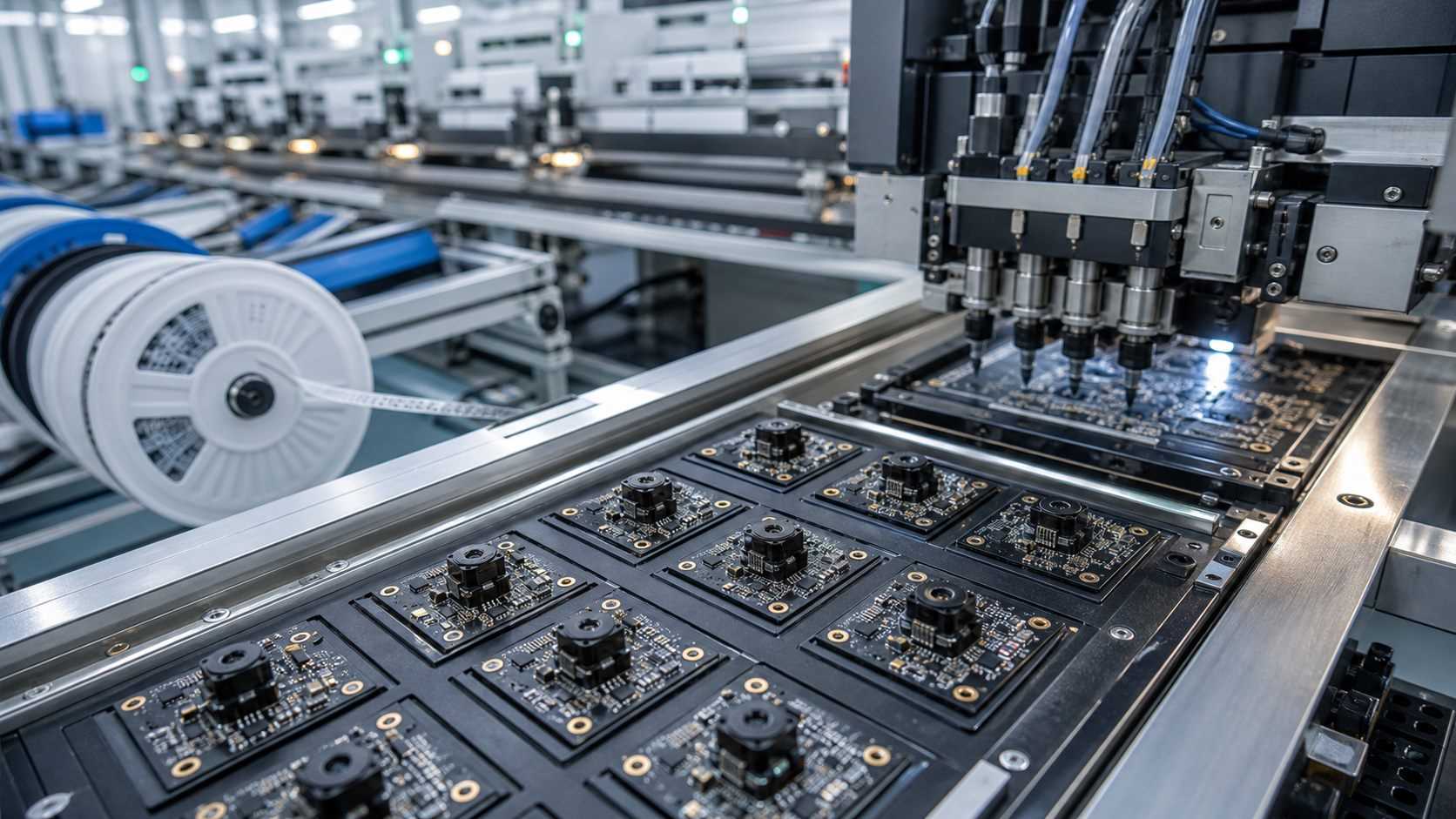
Camera module PCB assembly requires careful process control because the board often includes fine-pitch components, small connectors, sensor-related areas, and strict cleanliness requirements.
A typical camera module PCB assembly process may include:
- Engineering file review
- DFM and DFM-for-assembly check
- BOM review and component sourcing
- Bare PCB fabrication
- Incoming PCB and component inspection
- Solder paste stencil preparation
- Solder paste printing
- SMT placement
- Reflow soldering
- AOI inspection
- X-ray inspection when needed
- Connector or special component assembly
- Cleaning or cleanliness control when required
- Functional testing
- Final inspection and packaging
For camera PCB module projects, BOM quality is very important. Image sensors, connectors, FPC sockets, regulators, oscillators, capacitors, and protection components must match the project requirements. Wrong substitutes or unstable supply can delay production or affect reliability.
EBest Circuit provides turnkey support from PCB fabrication to component sourcing, SMT assembly, and testing. For engineering teams, this reduces communication gaps because the PCB, BOM, SMT, inspection, and test requirements can be reviewed together before production starts.
This one-stop workflow is especially useful for prototype and small-batch projects. Engineers can use the first build to validate the circuit, camera interface, mechanical fit, assembly process, and supplier readiness before moving into larger production.
Camera Module PCB Reliability Requirements
Camera module PCB reliability is critical because imaging products often work in real environments: heat, vibration, humidity, dust, motion, long operating time, and frequent power cycles.
Reliability requirements may include:
- Stable power supply to the sensor
- Low-noise signal routing
- Strong solder joint quality
- Reliable connector retention
- Controlled impedance for high-speed signals
- EMI and ESD protection
- Clean assembly around sensor-related areas
- Thermal management for long operation
- Mechanical stability around lens and sensor
- Traceable production and inspection records
For camera module PCB reliability, the manufacturer should not only inspect the finished board visually. The project may require AOI, electrical testing, functional testing, connector inspection, solderability review, and process traceability.
At EBest Circuit, quality control can be supported by ISO 9001, ISO 13485, IATF 16949, AS9100D, REACH, RoHS, and UL-related compliance systems. For production traceability, the digital workshop can track materials, product batches, production cycle, and production progress quickly. This helps engineering teams manage repeat orders, quality feedback, and delivery schedules more confidently.
Reliability also starts before production. DFM analysis, BOM optimization, and process adaptation suggestions can prevent many issues before parts are purchased or boards are assembled.
IP Camera Module PCB Board Applications
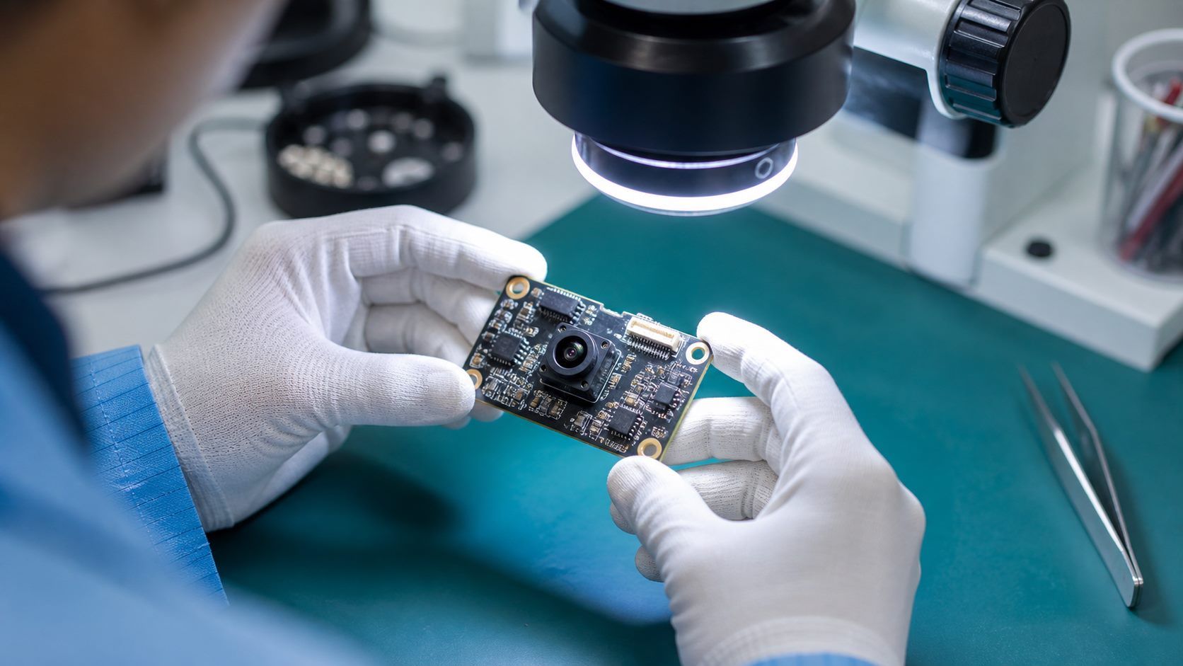
An IP camera module PCB board is used in network-connected imaging products. These products may need image capture, power management, data transmission, storage, wireless connection, LED control, audio, or motion detection functions.
Common IP camera and imaging applications include:
- Security cameras
- Smart doorbells
- Indoor monitoring cameras
- Outdoor surveillance systems
- Industrial vision modules
- Robot vision systems
- Drone camera modules
- Embedded camera devices
- AI camera modules
Compared with a simple camera board, an IP camera module PCB board may have more requirements for power, network interface, thermal management, EMI control, and long-term reliability. If the product works outdoors or in industrial conditions, humidity, temperature, enclosure design, and connector reliability should also be reviewed.
For manufacturing, IP camera projects often require more than one PCB. A complete system may include a camera module PCB, main control PCB, LED board, power board, wireless module, or connector board. A supplier with PCB and PCBA integration experience can help coordinate these boards and reduce assembly mismatch.
How to Choose a Camera Module PCB Manufacturer
Choosing a camera module PCB manufacturer should not be based only on unit price. Camera modules are compact, signal-sensitive, and assembly-sensitive. A low-cost supplier without engineering review may create higher cost later through rework, unstable quality, or delayed delivery.
When choosing a camera module PCB manufacturer, engineers should check:
- Can the manufacturer support both PCB fabrication and PCBA?
- Can they review Gerber files, BOM, pick-and-place files, and assembly drawings?
- Do they understand camera module PCB assembly requirements?
- Can they support flexible PCB for camera module projects if needed?
- Can they source components or work with customer-supplied materials?
- Do they provide DFM analysis and BOM optimization suggestions?
- Can they support prototypes, samples, and small-batch production?
- What testing and inspection methods are available?
- Are quality certifications and traceability systems in place?
- Can they respond quickly when engineers need technical feedback?
EBest Circuit is built for this type of engineering-driven project. The service model combines one business contact with a three-engineer technical support team to respond to customer needs across PCB, PCBA, BOM, and manufacturing process questions.
This is useful when the customer is not simply buying a bare PCB, but trying to bring a camera PCB module from engineering validation to reliable production.
Why Choose EBest Circuit as Your Camera Module PCB Manufacturer
A camera module PCB manufacturer should help engineers reduce risk before production, not only produce boards after the files are released. Camera PCB module projects often involve high-speed signals, compact board space, sensitive sensor areas, FPC connectors, impedance requirements, SMT assembly, and strict cleanliness control. These details need engineering review before the first batch is built.
EBest Circuit supports camera module PCB projects with:
- DFM pre-review before PCB fabrication
- BOM optimization and component availability review
- PCB manufacturing, component sourcing, SMT assembly, and testing
- Support for samples, prototypes, and small-batch production
- PCB and PCBA engineering feedback from experienced engineers
- ISO 9001, ISO 13485, IATF 16949, AS9100D, REACH, RoHS, and UL-related quality support
- Own PCB and PCBA factory plus more than 1,000 supply chain partners
- Digital production tracking for material batch, production status, and delivery progress
For engineers, this means fewer communication gaps between PCB fabrication, component sourcing, SMT assembly, and final testing. When the project needs fast validation, EBest Circuit can help prepare a practical path from camera module PCB prototype to reliable PCBA delivery.
Camera PCB Module Case Study for Thailand Security Cameras
One customer planned to use the camera module in Thailand, where outdoor security products may face heat, humidity, rain exposure, and sealed-housing conditions. For this project, the customer was not only asking for a 4 layer PCB. They needed a camera PCB module build that could support stable image transmission, SMT assembly, clean board surfaces, and reliable delivery for validation.
| Item | Project Requirement |
|---|---|
| Application | Security camera module for Thailand |
| PCB | 4L FR4, Tg130, 1oz copper |
| Finish | ENIG, black solder mask, white silkscreen |
| Thickness | 1.6mm +/-10% |
| Signal | 14mil trace, 50-ohm single-ended impedance |
| Assembly | SMT, single-board packing |
| Quality note | No solder balls or visible residue |
EBest Circuit reviewed the board as part of a camera product, not as a simple PCB order. If the module is used for HD, 4K, or higher frame-rate video, the PCB must support clean signal transmission. Our team checked the stackup, copper, dielectric thickness, and impedance requirement before production, with an impedance coupon and test report planned in advance.
We also reviewed the BOM, placement file, connector areas, and SMT notes before assembly. Camera module PCBs often use small components and sensitive connector areas, so soldering quality and post-SMT cleanliness matter. After assembly, each board needed inspection before individual packing.
Because the product was for Thailand, environment was part of the discussion. Tg130 FR4 may be suitable for many standard builds, but hot or humid outdoor use may require higher heat resistance, conformal coating, waterproof housing support, or stronger connector protection. These points should be confirmed before production, not after testing fails.
For the customer, the value was clear: EBest Circuit kept the impedance, material, SMT, cleanliness, packing, and environment-related risks connected from DFM review to shipment. The result was a camera PCB module build better prepared for product validation and small-batch delivery.
FAQs about Camera PCB Module
What is a camera PCB module?
A camera PCB board module is a printed circuit board assembly that supports camera-related components such as the image sensor, lens interface, connector, power circuit, passive components, and signal routing. It helps the camera capture, process, and transmit image data.
How do you find a camera lens and module on a PCB?
On a camera PCB, the lens is usually the round optical part mounted above or near the image sensor. The camera module area often includes the lens holder, image sensor, FPC or board-to-board connector, small passive components, and power or signal circuits around the sensor. In a finished product, the lens may face outward through the housing, while the PCB sits behind it.
What is the difference between a PCB camera module and a camera module PCB?
The terms are often used interchangeably. A PCB camera module usually refers to a camera module built around a PCB platform, while camera module PCB may refer specifically to the bare or assembled PCB used inside the camera module.
What affects camera module PCB assembly quality?
Assembly quality is affected by PCB pad design, solder paste printing, SMT placement accuracy, component quality, reflow profile, connector soldering, cleanliness, AOI inspection, functional testing, and process control.
What files are needed for a camera PCB module quote?
Usually, the manufacturer needs Gerber files, drill files, PCB specifications, BOM, pick-and-place files, assembly drawings, testing requirements, and any special notes about connectors, FPC, lens module, or sensor-related areas.
Can EBest Circuit support camera module PCB manufacturing and assembly?
Yes. EBest Circuit can support PCB fabrication, component sourcing, SMT assembly, DFM review, BOM optimization, testing, and small-batch or production delivery for camera module PCB and PCBA projects.
Ready to Build Your Camera PCB Module?
If you are developing a camera PCB module, PCB camera module, IP camera module PCB board, or flexible PCB for camera module project, EBest Circuit can help review the files and prepare a practical manufacturing path.
Send your Gerber files, BOM, pick-and-place file, drawings, or early project questions to sales@bestpcbs.com. Tell us what you are building, what stage you are in, and what you need to verify first. Our team will help you move from engineering files to reliable camera module PCB production with care and speed.