





A Bluetooth Module is small, but its PCB board has a direct effect on final wireless performance. Antenna clearance, grounding, power stability, impedance control, SMT quality, and testing all affect how well the product connects in real use.
This guide is written for engineers, buyers, and product teams who want to build a reliable Bluetooth PCB board, Bluetooth module board, or Bluetooth-enabled PCBA without spending too much time on generic theory.
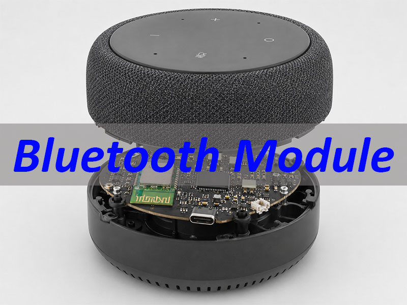
What Is a Bluetooth Module?
A Bluetooth Module is a compact wireless communication unit used to send data, audio, or control signals between electronic devices.
It usually includes:
| Part | Function |
|---|---|
| Bluetooth chip | Handles wireless communication |
| Antenna or antenna pad | Sends and receives RF signals |
| Crystal oscillator | Supports stable timing |
| Matching circuit | Helps RF signal transfer |
| Power circuit | Provides clean voltage |
| Interface pins | Connects with MCU or main board |
A module is easier to integrate than a bare Bluetooth chip because most RF-related parts are already built into the module.
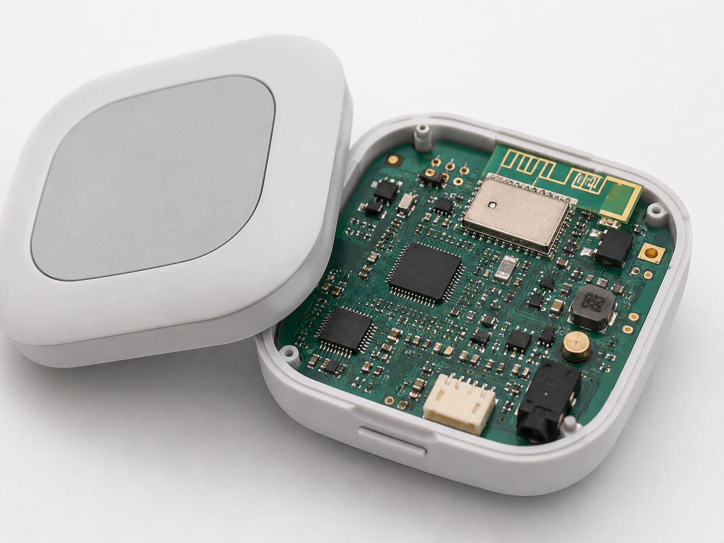
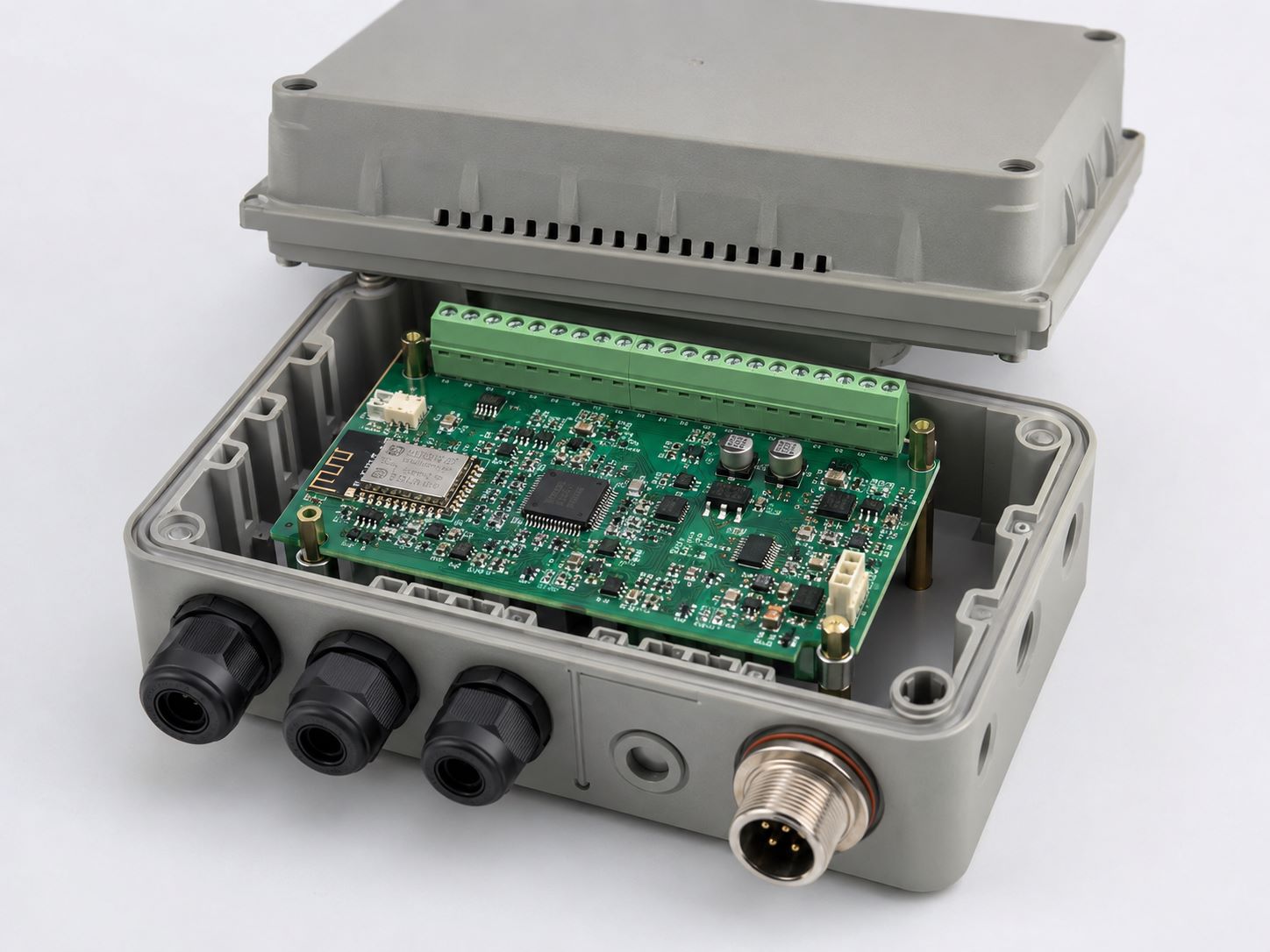
How Does a Bluetooth Module Work?
A Bluetooth module converts device data into a short-range wireless signal and sends it through the antenna.
In a real product, the signal path usually works like this:
- The MCU sends data to the Bluetooth module through UART, SPI, USB, or I2C.
- The module processes the data through the Bluetooth protocol.
- The RF circuit sends the signal through the antenna.
- Another Bluetooth device receives and decodes the signal.
- The device responds, pairs, or exchanges data.
For stable communication, the PCB must support clean power, good grounding, correct antenna placement, and controlled RF layout.
What Types of Bluetooth Modules Are Commonly Used?
Different products use different Bluetooth modules. The right choice depends on data type, power consumption, size, connection distance, and certification requirements.
| Type | Common Use |
|---|---|
| Classic Bluetooth module | Audio, serial data, legacy devices |
| Bluetooth Low Energy module | Wearables, sensors, IoT devices |
| Dual-mode Bluetooth module | Products needing Classic Bluetooth and BLE |
| WiFi Bluetooth module | Gateways, smart home devices, connected terminals |
| Bluetooth audio module | Speakers, headphones, voice devices |
| HC-05 / HC-06 module | Arduino, MCU learning, simple serial communication |
| HM-10 module | BLE-based low-power projects |
For commercial products, module selection should also consider supply stability, antenna type, firmware support, lifecycle status, and long-term availability.
Bluetooth Module vs Bluetooth Chip: What Is the Difference?
A Bluetooth chip is the core IC. A Bluetooth module is a more integrated wireless unit.
| Item | Bluetooth Chip | Bluetooth Module |
|---|---|---|
| Integration level | Low | Higher |
| RF design work | More complex | Easier to integrate |
| Certification path | More work | Often simpler |
| PCB layout difficulty | Higher | More manageable |
| Best for | Custom RF design | Faster product development |
A Bluetooth system on a chip may include RF, processor, memory, and protocol functions in one IC. A Bluetooth module usually places that chip with the required RF circuit, antenna, and supporting components on a small PCB.
For many product teams, the module route saves engineering time and reduces layout risk.
How Does a Bluetooth Module Connect to a Bluetooth PCB Board?
A Bluetooth PCB board turns the module into a working product circuit. This is where wireless performance meets manufacturing quality.
Key layout points include:
- Keep the antenna area away from copper, metal parts, tall components, and noisy circuits.
- Reserve proper antenna clearance according to the module datasheet.
- Use a clean ground plane to improve signal stability.
- Place decoupling capacitors close to the power pins.
- Keep high-speed or noisy digital traces away from RF areas.
- Control impedance when the design uses RF traces, USB, or other high-speed signals.
- Review grounding, shielding, and power routing before PCB fabrication.
With customer schematics, BOM, and mechanical requirements, EBest Circuit supports PCB layout optimization, PCB fabrication, component sourcing, SMT assembly, and functional testing for Bluetooth module board projects.
What Bluetooth PCB Board Manufacturing Capabilities Support Bluetooth Module Projects?
A Bluetooth PCB board is usually small, dense, and sensitive to signal consistency. For this type of project, customers mainly care about five manufacturing points: board size, routing density, via structure, signal control, and assembly reliability.
EBest Circuit supports Bluetooth module board projects with the following focused capabilities:
1. Compact Board Build for Small Wireless Devices
Bluetooth products are often used in wearables, smart sensors, handheld terminals, medical monitors, and IoT devices. These products usually leave very limited PCB space.
- Standard finished board size can reach 10 × 10mm.
- Prototype review can support smaller boards down to 3 × 3mm, depending on the design structure.
- Standard board thickness supports 0.4–6.0mm.
- Prototype review can cover 0.15–10mm when special thickness is required.
This is useful when the Bluetooth module board must fit into a compact enclosure while still carrying the module, MCU, power circuit, connector, and antenna-related layout.
2. Fine-Line Capability for Dense Bluetooth Circuits
Bluetooth PCB boards often combine wireless modules, MCUs, sensors, connectors, shielding parts, and small passive components on one compact board. Fine routing capability helps keep the layout manufacturable.
- Inner layer line width/spacing can reach 3/3mil at 1/2oz copper.
- Outer layer line width/spacing can reach 3.5/4mil at 1oz copper.
- Prototype review can evaluate finer routing, such as 2.5/2.5mil inner layers and 3/3mil outer layers.
This supports dense routing around Bluetooth chips, module pins, MCU areas, and compact component groups.
3. HDI and Via Support for Space-Limited Layouts
When the board becomes smaller, standard routing may not leave enough space. HDI structures and laser vias can help release routing channels and improve layout flexibility.
- Standard laser via size can reach 0.10mm.
- Prototype review can evaluate laser vias down to 0.070mm.
- Mechanical finished holes support 0.15–6.5mm.
- Standard through-hole aspect ratio supports up to 12:1.
This capability is valuable for mini Bluetooth PCB boards, multilayer wireless boards, and compact Bluetooth module board layouts.
4. Signal-Control Support for Bluetooth and High-Speed Interfaces
Some Bluetooth boards include USB, RF-sensitive traces, high-speed digital interfaces, or antenna-related layout areas. These designs require controlled material choice and impedance review.
- Supported materials include normal Tg FR4, mid Tg FR4, High-Tg 170–180 materials, high-speed low-loss materials, Rogers 4003/4350B, and PTFE high-frequency materials.
- Standard impedance tolerance supports ±5Ω for impedance below 50Ω.
- For impedance of 50Ω or above, standard tolerance supports ±10%.
This helps Bluetooth PCB board projects maintain more stable signal paths when the design includes RF-related routing, USB communication, or sensitive wireless areas.
5. Assembly-Ready Surface Finish and PCB Testing
Bluetooth PCBA often uses fine-pitch ICs, compact module pads, small passive parts, connectors, and shielding-related components. The PCB surface finish must support stable soldering and inspection.
- Surface finish options include ENIG, lead-free HASL, immersion tin, immersion silver, OSP, hard gold, soft gold, ENEPIG, and gold finger.
- For fine-pitch Bluetooth PCBA, ENIG is commonly used.
- ENIG thickness supports 0.025–0.125μm gold and 3–8μm nickel.
- PCB electrical testing can support up to 5000V DC / 3000V AC, depending on project requirements.
These capabilities help improve solderability, reduce assembly risk, and support more reliable Bluetooth module board production.
With these manufacturing capabilities, EBest Circuit can support FR4 Bluetooth PCB boards, multilayer Bluetooth boards, HDI wireless boards, controlled impedance boards, thin PCB boards, and high-frequency material Bluetooth boards from prototype to batch production.
Bluetooth Module Board Case Study: 6-Layer FR4 PCB with Blind and Buried Vias
Here is one Bluetooth module board we manufactured for a compact wireless device. The project used a 6-layer FR4 structure with Tg170 material, blind and buried vias, and a 50 Ohm impedance requirement on the front side.
The board thickness was controlled at 0.83mm ±0.1mm, helping the customer keep the product compact while still supporting multilayer routing. The design also used L1-L2 blind vias and L2-L3 buried vias, which helped release routing space around dense signal and component areas.
For the RF-related signal path, the board required 50 Ohm controlled impedance, with 0.11mm line width, 0.18mm line spacing, and L2 as the reference layer. The final PCB used white solder mask, black silkscreen, and ENIG 1u” surface finish for stable assembly and clean appearance.
This case shows EBest Circuit’s capability to support Bluetooth module boards with thin multilayer structure, HDI via design, impedance control, and production-ready surface finish.
Project Parameters
- PCB Type: 6-layer FR4 Bluetooth module board
- Material: FR4 Tg170, Shengyi material available
- Copper Thickness: 1oz inner layers and outer layers
- Board Thickness: 0.83mm ±0.1mm
- Via Structure: Blind and buried vias
- Blind Via: L1-L2
- Buried Via: L2-L3
- Impedance: 50 Ohm on front side
- Impedance Line Width: 0.11mm
- Impedance Line Spacing: 0.18mm
- Reference Layer: L2
- Solder Mask / Silkscreen: White solder mask, black silkscreen
- Surface Finish: ENIG 1u”
Where Are Bluetooth Module Boards Used?
Bluetooth module boards are used wherever devices need short-range wireless connection.
| Industry | Application Examples |
|---|---|
| Medical devices | Wearable monitors, portable diagnostic tools, wireless sensor units |
| Industrial control | Data collection terminals, wireless control panels, PLC adapters |
| Consumer electronics | Speakers, headphones, smart remotes, smart home devices |
| Automotive electronics | Diagnostic tools, infotainment modules, wireless controllers |
| IoT devices | Smart locks, asset trackers, gateways, environmental sensors |
| New energy | BMS communication boards, charger control modules |
| Robotics | Handheld controllers, sensor boards, wireless control units |
| Instruments | Portable meters, test devices, wireless data loggers |
For these products, stable Bluetooth communication depends on both module selection and PCB/PCBA manufacturing control.
Why Choose Us for Bluetooth Module Board Manufacturing?
Choose EBest Circuit when your Bluetooth product requires more than simple PCB fabrication. We support PCB layout optimization, PCB fabrication, component sourcing, SMT assembly, inspection, and functional testing for Bluetooth module board projects.
For different Bluetooth products, we can support a wide range of PCB structures, including FR4 rigid PCB, multilayer PCB, HDI PCB, flexible PCB, rigid-flex PCB, High-Tg PCB, controlled impedance PCB, and thin PCB. These board types are commonly used in compact wireless devices, smart home products, wearable electronics, industrial control terminals, medical monitoring devices, IoT gateways, automotive diagnostic tools, and battery management communication boards.
Our manufacturing support focuses on the details that directly affect Bluetooth module board performance:
- Antenna area review to help keep copper, metal parts, and noisy circuits away from sensitive RF zones.
- Grounding and power routing review to support cleaner power delivery and more stable wireless communication.
- Controlled impedance support for boards with USB, RF traces, or high-speed signal paths.
- DFM check before production to reduce layout, soldering, panelization, and assembly risks.
- Component sourcing and BOM checking to help confirm module availability, package compatibility, and alternative options.
- SMT assembly for compact wireless boards, including fine-pitch ICs, small passive parts, connectors, sensors, and shielding-related components.
- Inspection and testing support, including AOI, X-ray, electrical testing, and functional testing according to project requirements.
- Prototype, small-batch, and mass production support for different product development stages.
For Bluetooth module board projects, our role is simple: help turn your design files into a stable, manufacturable, and testable wireless PCBA.
Send your Bluetooth PCB board files or BOM to sales@bestpcbs.com for a manufacturing review and quotation.
FAQs about module bluetooth
Q1. What is a module bluetooth used for?
A module bluetooth is used for wireless data transfer, audio transmission, device pairing, remote control, and IoT communication. In product manufacturing, it is usually mounted on a Bluetooth PCB board or integrated into a larger PCBA.
Q2. Is a Bluetooth module the same as a Bluetooth chip?
No. A Bluetooth chip is the main IC. A Bluetooth module usually includes the chip, antenna, RF circuit, crystal, and supporting components, making it easier to integrate into a product.
Q3. What is the difference between HC-05 and HC-06 Bluetooth module?
HC-05 can usually work as master or slave. HC-06 is commonly used as a slave module. Both are popular for simple serial communication and Arduino projects.
Q4. Can a Bluetooth module be used in industrial control devices?
Yes. Bluetooth modules can be used in industrial data terminals, wireless panels, monitoring devices, and sensor communication boards. The PCB layout and assembly quality should support stable operation.
Q5. How do you test whether a Bluetooth module is working?
Common checks include power-on test, pairing test, serial communication test, signal response test, current consumption check, and product-level functional test.
Q6. What affects the range of a Bluetooth module?
The main factors include Bluetooth class, antenna layout, ground plane, power stability, enclosure material, nearby metal parts, and the actual working environment.
Planning a Bluetooth Module PCB board project? Just feel free to send your files or BOM to sales@bestpcbs.com, and our engineering team will help review the manufacturing details before production.







