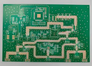
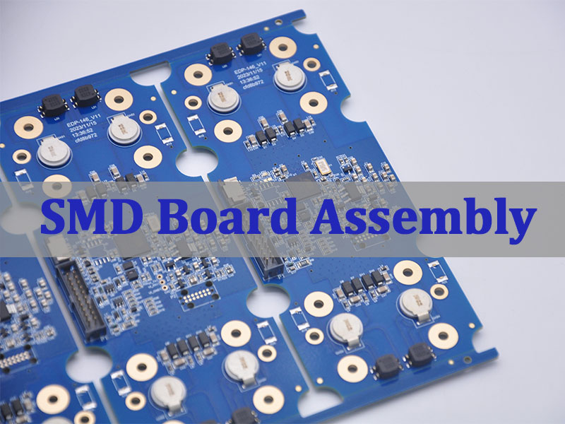
A battery cell monitoring system helps a battery pack collect cell-level voltage, temperature, and status data so the control system can make safer decisions. In electric mobility, energy storage, industrial backup power, test equipment, and smart battery products, a weak monitoring board can turn a promising pack into a difficult validation project.
For engineers and buyers, the practical question is not only how the monitoring circuit works. The harder question is whether the PCB, connectors, sampling paths, insulation spacing, component sourcing, SMT assembly, coating, testing, and packing can stay controlled from the first prototype to small-batch production.
EBest Circuit (Best Technology) supports battery-related PCB and PCBA projects with PCB fabrication, BOM sourcing, SMT assembly, inspection, functional test coordination, and manufacturing review. If you already have Gerber files, BOM, stackup, connector notes, test requirements, or assembly drawings, send them to sales@bestpcbs.com for an engineering review before production starts.
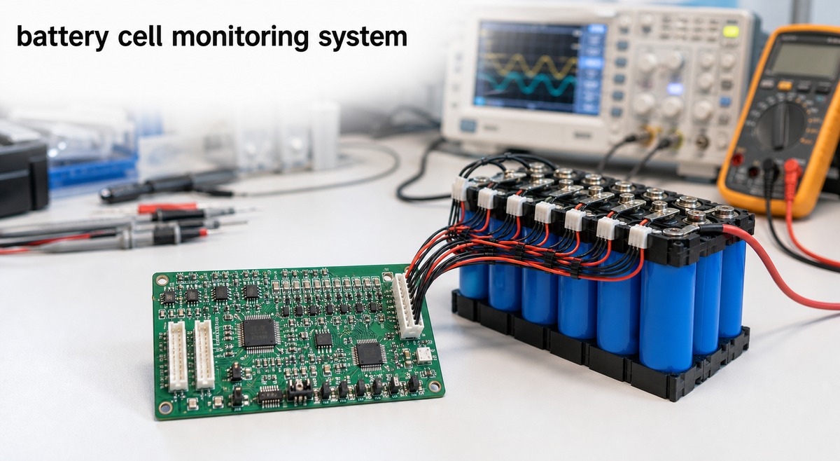
What Is a Battery Cell Monitoring System?
A battery cell monitoring system is the part of a battery pack that observes individual cell conditions and sends that information to the battery management system or control unit. It may monitor cell voltage, temperature, balancing status, communication signals, and fault-related conditions.
On the PCB side, this usually means the board must connect safely to many cells, route small sensing signals cleanly, keep high-voltage and low-voltage areas separated, and allow the assembled board to be tested before shipment.
For a real PCBA project, the files should make these points clear:
- cell count and connector pin order;
- cell voltage sampling paths;
- temperature sensor locations;
- battery monitoring chip part number;
- communication interface, such as CAN, UART, SPI, or isolated communication;
- creepage, clearance, slots, coating, or insulation requirements;
- test method and pass/fail criteria;
- packing method for assembled boards.
This article does not try to replace the customer’s battery algorithm, pack architecture, or protection strategy. It focuses on the manufacturing details that decide whether a released battery cell monitoring system board can be built and verified reliably.
Battery Cell Monitoring System vs Battery Management System
A battery cell monitoring system and a battery management system are closely related, but they are not always the same scope. Many search results use these terms together, so it helps to separate the board-level manufacturing view from the full system view.
| Term | Practical Meaning |
| Battery cell monitoring system | Measures cell-level data |
| Battery management system | Controls protection and pack behavior |
| BMS PCB | PCB used inside a BMS product |
| Monitoring PCBA | Assembled board for sensing and communication |
A full BMS may include protection logic, balancing strategy, current sensing, contactor control, state estimation, communication, firmware, and safety decisions. The monitoring board may be one part of that system.
For PCB and PCBA manufacturing, the responsibility should be clear. The customer defines the electrical design, monitoring IC, firmware, pack architecture, and safety logic. The PCB/PCBA supplier checks whether the released files can be fabricated, assembled, inspected, and tested according to the agreed production requirements. For broader background, this related guide explains what a BMS PCB board is.
Battery Cell Voltage Monitoring System for Accurate Readings
A battery cell voltage monitoring system depends on small voltage differences that must be routed from the pack connector to the monitoring IC without avoidable assembly or manufacturing errors. A wrong connector pin order, unclear net name, poor soldering, missing test pad, or contaminated connector area can make debugging painful.
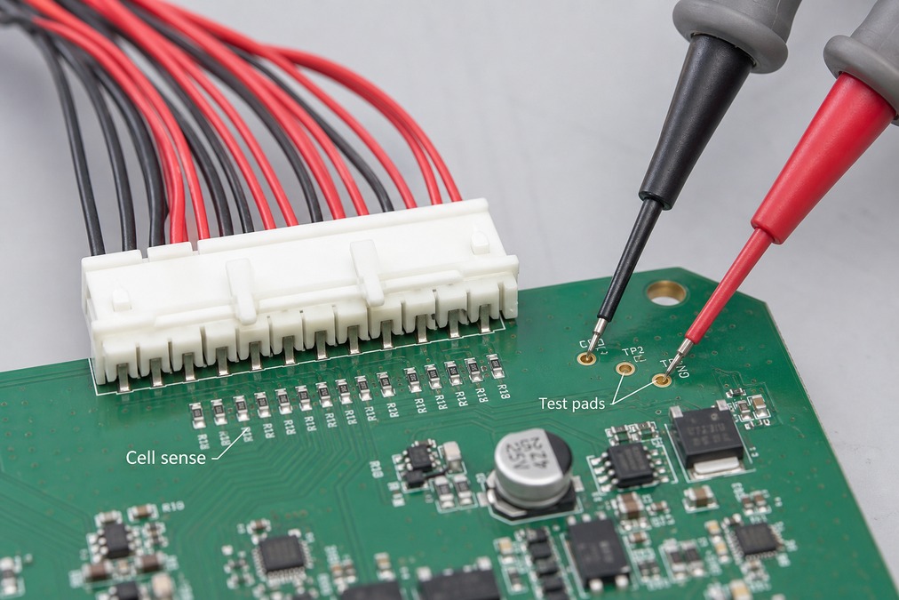
Before production, useful checks include:
- matching the connector drawing with the PCB footprint;
- checking connector orientation and pin 1 location;
- confirming test pads for key sensing nets;
- reviewing resistor and capacitor placement near the sampling path;
- checking solder mask openings around dense connector pins;
- making sure sampling nets are not confused during harness assembly;
- confirming inspection access after SMT.
If the first prototype shows unstable cell readings, the root cause may not be the monitoring IC itself. It may be a connector issue, soldering defect, poor test access, wrong component value, or file mismatch. That is why BOM, Gerber, CPL, connector drawing, and test notes should be reviewed together.
Cell Monitoring System PCB Interfaces That Reduce Assembly Risk
A cell monitoring system is usually connector-heavy. The PCB may connect to cell taps, NTC thermistors, pack current paths, communication lines, programming pads, external harnesses, and sometimes an enclosure or shield structure. Each interface is a possible failure point if the drawings are incomplete.
The most useful interface details are the ones that prevent rework:
- connector series, pitch, height, locking direction, and mating part;
- wire harness direction and keep-out areas;
- current rating for power or balancing paths;
- mechanical support for heavy connectors;
- test access for production verification;
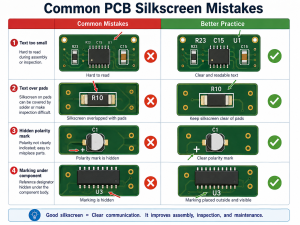
- polarity and pin sequence markings;
- packing protection for exposed connector pins.
For buyers, this is where a one-stop PCB and PCBA workflow reduces handoff risk. If PCB fabrication, component sourcing, SMT, through-hole soldering, cleaning, inspection, and packing are coordinated separately, connector notes can be missed. EBest Circuit keeps these notes visible from file review to shipment.
Battery Monitoring Chip Placement for Stable PCBA Performance
A battery monitoring chip is often the most important IC on the board. Its placement affects sensing trace length, filter component placement, isolation strategy, thermal exposure, programming or communication access, and inspection after SMT.
EBest Circuit does not choose the customer’s monitoring chip or define the battery algorithm. The approved IC, circuit, and firmware come from the customer’s engineering team. The manufacturing review focuses on whether the selected package, footprint, BOM data, and assembly files match the physical build.
Typical PCBA risks around the monitoring IC include:
- wrong IC package or footprint version;
- pin 1 mismatch between datasheet, PCB footprint, and CPL file;
- fine-pitch solder bridging;
- insufficient solder on small passives near the IC;
- missing test access for communication or programming;
- thermal exposure from nearby power components;
- unclear firmware or test-step requirements.
If the project includes customer-provided firmware or programming files, the programming method and verification step should be defined before assembly. For related production flow, this article on IC programming explains how firmware loading can fit into PCBA production.
Battery Monitoring System PCB Safety for High-Voltage Packs
Battery monitoring system PCB safety becomes more important as cell count, pack voltage, and enclosure constraints increase. A monitoring board may carry only sensing current, but it can still connect to high pack potential through the cell tap harness. Manufacturing details must respect the customer’s released safety spacing and insulation requirements.
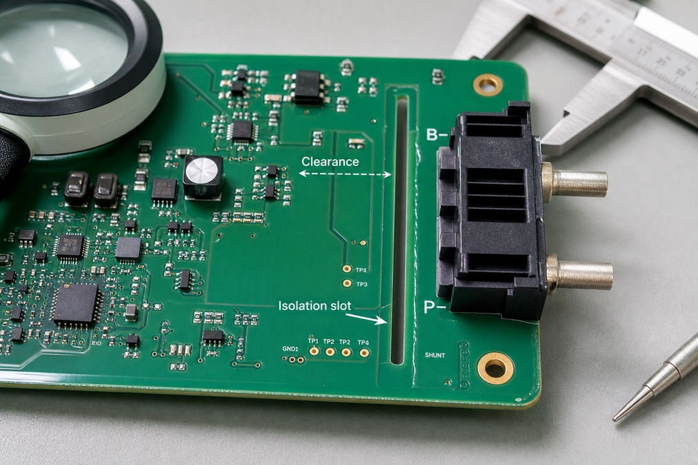
Safety-related PCB manufacturing points may include:
- creepage and clearance between cell groups;
- slots, cutouts, or keep-out areas;
- solder mask dams and exposed copper control;
- board thickness and mechanical stiffness;
- surface finish and solderability;
- conformal coating or potting notes;
- connector spacing and insulation barriers;
- mounting hole clearance from high-voltage nets.
The PCB manufacturer should not change the safety spacing or net relationships without approval. However, the supplier should flag unclear drawings, missing slots, tight copper spacing, or coating conflicts before production. For boards used in sealed or harsh environments, PCB encapsulation or conformal coating requirements should also be reviewed before assembly.
Battery Management System Cell Monitoring Diagram Before Production
A battery management system cell monitoring diagram is useful only when it can be translated into clear PCB and PCBA files. A diagram may show cell taps, sense resistors, NTCs, isolation, communication, balancing circuits, and pack connectors, but the factory still needs released manufacturing data.
Before quotation or production, prepare:
- Gerber or ODB++ files;
- NC drill files;
- stackup and finished board thickness;
- BOM with manufacturer part numbers;
- CPL or pick-and-place file;
- assembly drawing;
- connector drawings and mating connector notes;
- coating, cleaning, and packing requirements;
- test instructions and acceptance criteria.
The diagram helps explain intent, but it should not replace production files. If a diagram and Gerber data conflict, the customer should confirm which document controls the build before PCB fabrication starts. The same principle applies to custom BMS PCB projects where the board must fit both electrical and mechanical requirements.
Battery Monitoring Unit Assembly for Prototype and Small-Batch Builds
A battery monitoring unit prototype is often small in quantity but high in consequence. One incorrect connector, one wrong resistor value, or one missing test point can delay pack validation and make the engineering team question whether the issue comes from the circuit, assembly, harness, or test setup.
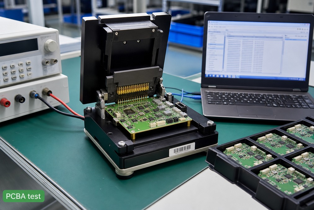
For prototype and small-batch PCBA, the useful production path is:
- review PCB files, BOM, CPL, drawings, and connector notes together;
- confirm unavailable or risky components before SMT scheduling;
- check polarity, pin 1, connector orientation, and test access;
- prepare SMT, through-hole, cleaning, and inspection steps;
- run AOI, visual inspection, and agreed functional checks;
- pack finished boards to protect connectors and exposed pins.
Small quantity does not remove process risk. A two-piece prototype still needs correct materials, controlled assembly, and usable inspection. For projects moving from prototype to pilot build, PCB assembly support should be aligned with the test plan and delivery schedule.
Battery Cell Monitoring System Case Study for a PCBA Project
A European customer needed a small-batch monitoring PCBA for an industrial battery pack used in energy storage validation. The customer had already released the electrical design, monitoring IC selection, and firmware. The main request was to build a small quantity of boards that could support stable connector contact, cell voltage sampling, communication testing, and clean inspection before pack-level validation.
Project snapshot:
- Customer region: Europe;
- Application: industrial energy storage battery module;
- Build type: prototype to small-batch PCBA;
- PCB: multilayer FR4 monitoring board;
- Key concerns: connector order, cell sampling stability, isolation spacing, SMT quality, and test access;
- Delivery need: engineering validation boards before next pack test round.
Manufacturing challenge:
- The board used dense connectors for cell tap inputs and temperature signals.
- Several sampling nets needed clear test access after assembly.
- Connector direction and harness routing had to match the customer’s enclosure plan.
- The project required a practical inspection path before the boards were packed.
EBest Circuit support:
- Reviewed Gerber data, BOM, CPL, assembly drawing, and connector notes together.
- Checked connector footprint, orientation, and polarity markings before SMT.
- Confirmed test pads for key sensing and communication nets.
- Coordinated PCB fabrication, component sourcing, SMT assembly, inspection, and packing under one workflow.
- Kept engineering questions visible before production rather than during final inspection.
The customer received assembled monitoring boards for pack validation with connector, sampling, inspection, and packing details controlled as one project. The value was not only receiving the boards. The value was reducing uncertainty before the customer connected the PCBA to a real battery module.
Why this matters for battery monitoring PCBA projects: battery monitoring builds are not forgiving. If the board has unclear connector notes, unstable sampling access, poor soldering, weak traceability, or missing test instructions, the customer may lose time during pack validation. EBest Circuit is useful when the buyer needs PCB fabrication and PCBA assembly details coordinated by one team.
Support that matters during a battery monitoring build:
- PCB fabrication and stackup review;
- BOM sourcing based on approved part numbers;
- SMT and through-hole assembly;
- connector and polarity review;
- AOI, visual inspection, and agreed test coordination;
- coating, cleaning, and packing notes when required;
- prototype, sample, and small-batch production support.
EBest Circuit has supported PCB and PCBA manufacturing since 2006, with ISO9001, ISO13485, IATF16949, AS9100D, RoHS, REACH, and UL-related quality support. For battery-related projects, that background helps keep file review, purchasing, assembly, inspection, and delivery communication connected.
FAQs About Battery Cell Monitoring System PCBA
1. Is a battery cell monitoring system the same as a BMS?
No. A battery cell monitoring system usually focuses on collecting cell-level data. A BMS has a broader role and may include protection, balancing, current measurement, firmware, communication, and pack control.
2. What files are needed for battery monitoring PCBA assembly?
Useful files include Gerber or ODB++, drill files, stackup, BOM, CPL, assembly drawing, connector drawings, coating notes, test requirements, and packing instructions.
3. Can EBest Circuit design the battery management algorithm?
No. The battery algorithm, pack architecture, protection logic, and firmware should come from the customer’s engineering team. EBest Circuit supports PCB fabrication, BOM sourcing, PCBA assembly, inspection, and agreed testing coordination.
4. Why are connectors important in battery cell monitoring boards?
The connectors carry cell tap, temperature, communication, or power-related signals. Wrong orientation, unclear pin order, weak soldering, or poor packing can create validation problems.
5. Should battery monitoring PCBAs be tested before shipment?
Yes. The test scope depends on the customer requirement, but visual inspection, AOI, connector checks, continuity-related checks, and agreed functional verification can reduce avoidable risk before delivery.
All in all, a battery monitoring board should arrive ready for the customer’s validation work, not as another source of uncertainty. If your next battery cell monitoring system project includes dense connectors, cell sampling paths, coating notes, test requirements, or small-batch PCBA assembly, send the released files to sales@bestpcbs.com. EBest Circuit can review the manufacturing path before the build moves into production.