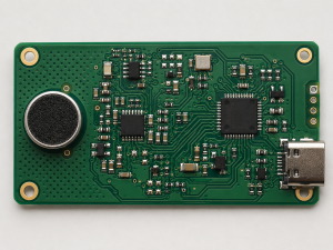
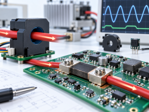
A car charger circuit board converts vehicle power into a stable USB output while protecting the connected device and managing charging behavior. The car charger circuit board combines an input protection stage, a DC-DC power stage, a charging or USB controller, filtering and the output connector in a compact space. This article covers low-voltage automotive USB charging modules used in plug-in, dashboard and center-console products, not EV traction-battery or onboard chargers.
The practical challenge is not simply making the USB port turn on. An automotive USB charger PCB must carry the required current without excessive voltage drop, remove heat from the switching components, survive the specified electrical environment and keep the connector mechanically stable. If your design files are ready, send the Gerber or ODB++, BOM, schematic, mechanical data and test requirements to sales@bestpcbs.com for a free DFM review.
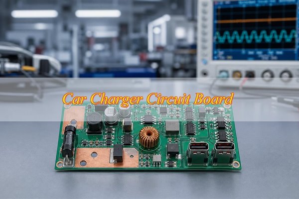
What Is a Car Charger Circuit Board and How Does It Work?
A car charger PCB is a compact power-conversion assembly that turns the vehicle supply into the voltage and charging behavior required at one or more USB ports. Power normally enters through the module connector, passes through protection and filtering, reaches the switching converter, and then flows through the charging controller or port controller to the USB output.
- Input protection: Limits damage from reverse connection, overvoltage, transient events or a short that the product specification requires the module to withstand.
- DC-DC conversion: Regulates the varying vehicle input to the output needed by the selected charging architecture.
- Charging control: Identifies or negotiates the permitted output behavior for USB-A, USB-C or USB Power Delivery.
- Filtering and grounding: Contain switching noise and give the power and control circuits a stable reference.
- Connector and enclosure path: Carry current to the cable, support insertion forces and help move heat away from the board.
These blocks work as one system. A capable controller cannot compensate for an undersized current path, and a large copper area will not solve a poor thermal connection beneath the power package. The design should therefore be reviewed from the vehicle input to the USB contact rather than as isolated components.
What Types of Car Charger PCBs Are Used for USB-A, USB-C and USB PD Modules?
The port type sets only part of the design; output behavior, available power, port count and mechanical format determine the actual circuit and assembly. Common USB car charger PCB variants include USB-A, USB-C, USB PD and multi-port boards. Two products can use the same connector while requiring different controllers, power stages, firmware and validation.
- USB-A charging boards: Commonly combine a regulated power stage with a charging-port controller and a mechanically supported receptacle. The layout must protect output voltage from cable and connector losses, while the assembly drawing defines connector position, shell tabs and orientation.
- USB-C charging boards: Add configuration and attachment-detection requirements. The smaller connector geometry and inaccessible joints may also change stencil design, inspection access and the method used to verify connector alignment.
- USB PD charging boards: Require a compatible power stage, PD controller and approved configuration for the profiles the product is intended to provide. USB-IF maintains the current USB Power Delivery specification; hardware, controller configuration and functional testing should refer to the same approved product requirement.
- Multi-port charging boards: Add power sharing, simultaneous-load behavior, denser connector placement and concentrated heat. Evaluate a dual-port board under the intended combined load rather than testing each port separately and assuming the same result.
What Electrical and Protection Requirements Affect a Car Charger Circuit Board?
The protection circuit must be selected from the customer’s defined input conditions and failure tests, not from a generic “automotive” label. Vehicle supply conditions vary by product and system. The RFQ should state the normal input range, abnormal-input conditions, transient requirements and recovery behavior that the finished module must meet.
- Reverse-polarity protection: Confirm how the circuit blocks or tolerates an incorrect supply connection and whether the selected device creates a significant voltage or thermal penalty.
- Overvoltage and transient protection: Coordinate the suppressor, switch and converter ratings so the first protection device does not merely pass excessive stress to the next part.
- Overcurrent and short-circuit behavior: Define the trip, limiting and recovery response at both the input and the USB output where applicable.
- Input and output filtering: Place the filter around the actual noisy current path and verify it with the target wiring, load and enclosure conditions.
- Connector-side protection: Review ESD and unintended voltage exposure at the user-accessible port as part of the product requirement.
The protection parts also influence placement and heat. For example, putting a suppressor close to the input connector can shorten its discharge path, but the surrounding copper, clearances and nearby heat-sensitive components still need to suit the specified stress. The right outcome is a coordinated protection path, not the maximum part rating in every position.
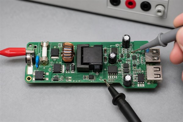
How Should the Power Layout Be Designed for a Car Charger PCB?
A reliable layout keeps the high-current path wide and continuous while making the switching loop physically small. The two goals are related but not identical. Current capacity depends on the complete conductor path; switching behavior depends heavily on loop area, component placement and the return path.
- Follow the power path: Review the route from input connector to protection device, converter, inductor, output capacitor and USB connector. Pad exits, thermal reliefs, via transitions and connector contacts can be more restrictive than the main trace.
- Minimize the switching loop: Place the switching device, inductor and high-frequency capacitors according to the controller manufacturer’s layout guidance. Keep sensitive feedback and configuration signals away from noisy nodes.
- Provide a deliberate return path: Avoid splitting the reference beneath critical control or high-frequency paths. Ground vias should support the intended current and thermal flow rather than being added without a clear function.
- Avoid copper neck-downs: Check changes in width at pads, fuses, shunts, vias and connector pins. Local loss and heat often appear where the conductor becomes narrow for only a short distance.
- Plan test access: Add stable measurement points for the input, regulated output, port output and key control nodes without disturbing the power loop.
During DFM, the layout should be checked against the finished copper, drill and assembly constraints that will actually be produced. A visually broad polygon is not proof of current capacity if its connection to a pad passes through a narrow spoke or an insufficient via group.
How Should Heat Be Managed in a Compact Car Charger PCB?
Thermal control starts by identifying where loss occurs and where that heat can leave the assembled module. The converter, MOSFETs, inductor, protection devices and connector contacts can all become limiting points. Their temperatures depend on conversion loss, conductor resistance, airflow, enclosure contact and how nearby heat sources interact.
- Copper spreading: Connect useful copper to the thermal pad or power node without enlarging the noisy switching node unnecessarily.
- Thermal vias: Move heat into useful copper on other layers; confirm drill size, finished hole condition and solder-control strategy with the manufacturer.
- Stencil apertures: Segment exposed-pad openings when needed to balance solder coverage, voiding risk and package seating.
- Component spacing: Keep electrolytic capacitors, plastics and other temperature-sensitive parts away from concentrated heat where the enclosure permits.
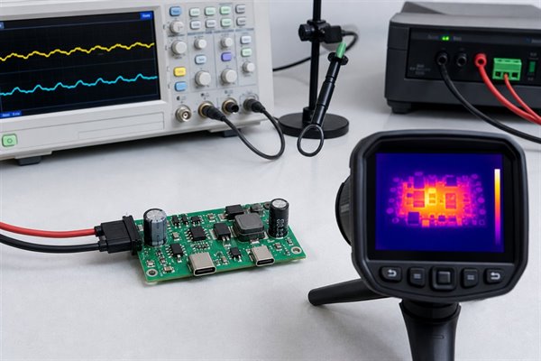
- Loaded measurement: Test the assembled module at defined loads and ambient conditions, then record the hottest component and voltage drop along the main power path.
A bench result with the bare board exposed may not represent a closed dashboard or console enclosure. If the product depends on a housing contact or metal heat path, that interface belongs in the validation setup and the mechanical drawing.
What PCB Materials, Copper Weight and Stackup Are Suitable for Car Charger PCBs?
FR-4 is a common starting material, but layer count, finished copper and board thickness should follow the electrical, thermal and mechanical needs of the specific module. There is no single construction that fits every car charger circuit board.
- When two layers may fit: A two-layer board can be practical when the power is moderate, component density is low, the ground return remains continuous and enough copper area is available for current and heat spreading. Verify voltage drop, hot spots and switching behavior on the assembled module.
- When four layers may help: Four layers become useful when the board needs a more continuous reference plane, denser routing, better separation of power and control paths, additional heat spreading or a smaller outline. Adding layers without assigning a function to them increases cost without guaranteeing better performance.
- What the drawing should control: State the laminate or approved material requirement, final thickness, layer count, finished copper, surface finish and stackup. Copper weight alone is not a current guarantee because a narrow pad exit, via transition, solder joint or connector contact can still create local resistance and heat.
- How to confirm the choice: Select the surface finish for the actual component, solderability, storage and customer requirements, then use fabricated-board and assembled-product results to verify that the selected construction meets the electrical, thermal and mechanical limits.
What DFM Checks Matter Before Car Charger PCB Manufacturing?
DFM should inspect the complete input-to-output path and its mechanical interfaces because current, thermal and connector failures often develop across more than one footprint. A useful review marks the exact feature, explains the possible failure and proposes a change that the customer can approve.
- Current-path continuity: Trace the input connector to the protection stage, regulator, inductor, output capacitor and USB connector. Check every neck-down, via group, thermal relief and high-current pad.
- Thermal-pad manufacturability: Review pad dimensions, via layout, solder-mask openings and stencil segmentation for power packages with exposed pads.
- Connector fit: Compare the footprint, shell tabs, centerline, board edge and enclosure opening. Confirm that placement and inspection remain possible after panelization.
- Assembly clearance: Check component spacing around the inductor, power devices and connectors for placement, soldering, rework and mechanical load.
- Inspection and test access: Identify hidden joints and decide whether visual inspection, AOI, X-ray, a mechanical gauge or a powered test can detect the relevant defect.
- File consistency: Cross-check Gerber or ODB++, drill data, BOM, centroid file, assembly drawing and mechanical model for revision, footprint and coordinate conflicts.
A focused car charger circuit board DFM review should distinguish a required correction from an optional cost or process suggestion. That distinction helps the buyer approve changes without turning every manufacturing preference into a product requirement.
How Is a Car Charger Circuit Board Manufactured and Assembled?
Manufacturing begins with the approved PCB construction and ends with an assembled, identified unit that can be tested against the intended charging behavior. The process route changes with the board design and component set, but the sequence should preserve product identity at every stage.
- CAM and panel review: Confirm the approved stackup, copper features, drill data, solder mask, finish and panel method before tooling. This check catches file or clearance conflicts that could create a fabrication defect before production records are issued.
- PCB fabrication: Build the layers, plated holes, solder mask and surface finish to the fabrication drawing. Bare-board electrical testing verifies the finished PCB for opens and shorts before assembly begins.
- Solder-paste printing: Set stencil apertures from the approved component and footprint data. Inspect the print where fine-pitch controllers, exposed thermal pads or large power pads create bridging, insufficient-paste or voiding risks.
- SMT placement: Place the power IC, MOSFETs, controller, inductor, capacitors and protection devices from the approved BOM with the correct orientation. Placement inspection catches a wrong, missing or shifted part before it creates a placement defect at reflow.
- Reflow soldering: Use a profile suited to the approved solder paste, board mass and package set. Review joint formation and exposed-pad behavior because poor wetting, voiding or package lift can create electrical and thermal failures.
- Connector and through-hole assembly: Install USB receptacles, input terminals and mechanically loaded parts according to the assembly drawing. Verify orientation, shell seating and solder joints to prevent a mechanical defect, retention failure or intermittent contact.
- Inspection, programming and functional test: Apply the methods required by package and product failure risks, then record results against the correct PCB, BOM and program identity. Failed or mismatched units remain separated until reviewed and dispositioned.
The manufacturing record should make substitutions, rework and program changes visible. This is especially important when several variants share the same bare PCB but use different components or charging configurations.
How Are USB-C, USB PD and Power Components Controlled During Assembly?
Assembly control must prevent visually similar parts or boards from leaving production with the wrong charging function. The BOM, placement data, program file and test profile should use a shared variant identifier.
- PD controller and configuration: Map each hardware revision to its approved configuration or firmware. Verify the loaded identity where programming is part of the build.
- Power IC and MOSFETs: Check the exact manufacturer part number, package, orientation and thermal-pad condition. Approved alternatives require an electrical and thermal review, not just footprint compatibility.
- Inductor and capacitors: Control electrical rating, package height, polarity where applicable and supplier-approved substitutions that can affect loss, heat or fit.
- USB connector: Confirm connector orientation, shell seating, mechanical tabs and solder joints. Hidden joints need an inspection method suited to their geometry.
- BOM revision: Keep consigned, turnkey and customer-approved components clearly separated so purchasing does not introduce an unreviewed alternative.
When one bare board supports several port or power variants, physical labeling and electronic identity should agree. Functional testing should then check the output behavior assigned to that variant rather than applying one generic test to every assembly.
How Should Car Charger PCBAs Be Inspected and Functionally Tested?
Inspection and testing should be selected by failure mode and production stage. No single method proves solder quality, firmware identity, charging negotiation, output stability and thermal performance.
- Before assembly: Bare-board electrical testing checks PCB opens and shorts.
- During assembly: SPI may be used when paste volume or alignment is a significant process risk. AOI or visual inspection can detect applicable placement, polarity and visible-joint defects.
- For hidden joints: X-ray may be applied to selected bottom-terminated packages, exposed pads or inaccessible connector joints when it can reveal the defined defect.
- After programming: A readback or identity check confirms the expected controller configuration where the product requires it.
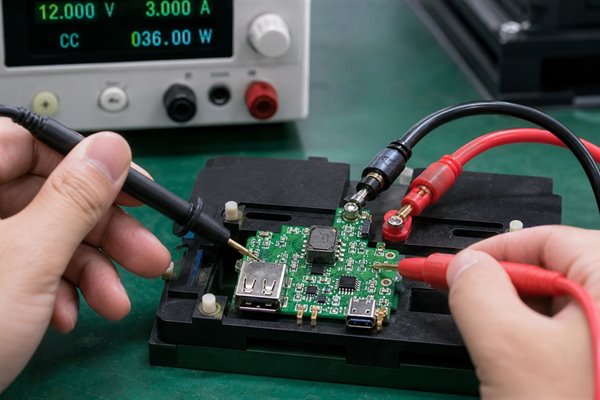
- Powered testing: No-load and loaded output, port detection, requested PD profiles and simultaneous-load behavior can be checked against customer-defined limits.
- Product validation: Temperature rise, transient response and EMI/EMC testing belong in the plan only when the applicable specification, setup and acceptance criteria are defined.
IPC J-STD-001J and IPC-A-610J address soldering process requirements and post-assembly acceptance, respectively. Purchase documents still need to name the applicable revision, class and customer-specific criteria. Functional testing complements those checks; it does not replace structural inspection.
What Common Car Charger PCB Failures Should Be Checked Before Mass Production?
Failure analysis should begin with the symptom and a reproducible operating condition because the same visible fault can come from the PCB, component, program, connector or test setup. Replacing a component or adding copper before locating the cause can hide the original defect and create a new one.
- Excessive temperature: Measure the converter, MOSFET, inductor, protection stage and connector under the intended load. Check whether loss comes from the component, copper path, solder joint or enclosure interface.
- Voltage drop: Measure before and after pad exits, vias, protection devices and connector contacts. The weakest short segment can dominate the total loss.
- Unstable charging or resets: Review input transients, loop layout, grounding, output capacitance, controller configuration and the test cable or load.
- USB recognition failure: Compare the installed controller, configuration resistors, firmware or PD profile with the intended variant.
- Connector solder cracking: Inspect shell tabs, mechanical support, board-edge position and enclosure loading rather than treating the joint as an electrical connection only.
- Weak multi-port performance: Test simultaneous load, power sharing and thermal concentration with both ports active.
- EMI-related instability: Review the high-frequency loop, filter placement, reference path and cable setup before changing the entire stackup.
A corrective action is ready for the next build only after the cause, affected units, design or process change and verification result are documented. If the same feature appears in another variant, the review should include that related board before volume release.
How Do You Move a Car Charger PCB From Prototype to Mass Production?
A prototype proves that the tested units can work; a pilot build proves that the intended files, materials, assembly route and test limits can produce repeatable units. The transfer does not need a long internal procedure, but it does need five items to remain aligned.
- PCB data: Update and freeze the Gerber or ODB++ after approved PCB changes.
- Component data: Freeze the BOM and record any approved substitutions.
- Program identity: Match the firmware or controller configuration to the hardware revision.
- Assembly definition: Carry the assembly drawing and connector datum used by the approved sample into the pilot package.
- Test limits: Use the same functional-test conditions and pass limits that supported the production decision.
The pilot should reveal undocumented rework, difficult connector assembly, variable thermal-pad soldering, unstable tests or material substitutions before they become volume problems. Once corrected, those changes need to appear in the files used for the next order, not only on a reworked sample.
What Files Are Needed for a Car Charger PCB Manufacturing Quote?
A quote becomes more accurate when the supplier can identify the PCB construction, installed components, mechanical interfaces and required tests from one consistent package. These files control the quoted material, tooling, assembly and test scope because each car charger PCB manufacturer is pricing the same product definition. At minimum, provide five groups:
- PCB data: Gerber or ODB++, drill files and fabrication drawing.
- Assembly data: BOM, centroid or pick-and-place file and assembly drawing.
- Electrical definition: Schematic, required USB functions and approved controller configuration or firmware where applicable.
- Mechanical definition: Board outline, connector datum, mounting points, height limits and enclosure interface.
- Commercial and test inputs: Prototype and volume quantities, sourcing responsibility, inspection requirements, powered-test conditions and expected records.
Open items can be listed instead of guessed. The supplier should return the assumptions that affect material, tooling, programming or test cost so quotations can be compared on the same scope.
Why Choose EBest Circuit for Car Charger PCB Manufacturing and Assembly?
EBest Circuit can combine PCB fabrication, component sourcing, SMT, through-hole and mixed assembly within one car charger PCBA project. The same project scope can keep the board construction, component identity, connector assembly and test requirements aligned from prototype through repeat production.
- Car-charger-specific DFM: The free review can identify current-path neck-downs, exposed-pad and stencil risks, connector alignment issues, assembly clearances and missing test access.
- PCB and PCBA coordination: Fabrication and assembly decisions can be reviewed against the same BOM, mechanical interface and variant definition.
- Component sourcing control: Manufacturer part numbers, customer-supplied items and approved substitution boundaries can be agreed before purchasing.
- Applicable inspection and testing: The proposed route can match visual inspection, SPI, AOI, X-ray, programming or functional testing to the actual package and product risks.
- Quality-system evidence: EBest holds IATF 16949 and ISO 9001:2015 certifications, together with RoHS and UL credentials. Buyers can request current documents and verify the covered legal entity, site and service scope for the proposed order.
The customer benefit is a clearer transition from design review to an assembled and testable product, with fewer gaps between the PCB files, BOM, controller configuration and acceptance requirements. Send the current package to confirm which capabilities and records apply to your specific module.
FAQs About Car Charger Circuit Boards
Q1: Is a car charger circuit board the same as an EV charger PCB?
A1: No, they serve different power systems. The board discussed here powers USB devices from a low-voltage vehicle supply. An EV onboard or traction-battery charger operates at a different voltage and power level and requires a different isolation, safety, control and validation architecture.
Q2: Does a USB-C connector automatically mean the board supports USB PD?
A2: No, the connector alone does not provide PD. USB-C defines the connector and interface framework. USB Power Delivery support also depends on a compatible controller, power stage, configuration and functional test that verifies the profiles approved for the product.
Q3: Can one car charger PCB support USB-A and USB-C ports?
A3: Yes, when both ports are designed as one power system. The board must allocate the available power, use the required charging controllers, maintain connector clearances and handle the combined heat. Simultaneous-load testing should confirm that one active port does not cause the other to fall outside its approved output behavior.
Q4: Is a four-layer PCB always better for a car charger?
A4: No, layer count should solve a defined design need. Four layers can improve reference continuity, routing density and heat spreading, but a well-designed two-layer board may be suitable when current, space and EMI requirements allow it. Assign a purpose to each added layer before accepting the extra cost.
Q5: What usually causes a car charger PCB to overheat?
A5: Overheating usually comes from several losses adding together. Common contributors include converter loss, an undersized copper or via path, poor exposed-pad soldering, unsuitable inductor or MOSFET selection, connector resistance and an ineffective enclosure heat path. Loaded temperature measurements can identify which location limits the design.
Q6: Why can output voltage be correct with no load but low during charging?
A6: The load reveals resistance that a no-load check cannot show. Protection devices, copper neck-downs, vias, solder joints, connectors and cables can each contribute voltage drop. Measure before and after each segment under the intended load instead of increasing copper everywhere without locating the loss.
Q7: Does AOI prove that a car charger PCBA will charge correctly?
A7: No, AOI verifies only suitable visible features. It can detect applicable placement, polarity and solder-joint defects, but it cannot prove the controller configuration or charging response. Correct charging behavior requires the intended components and program plus a powered functional test with defined limits.
Q8: When is X-ray inspection useful?
A8: Use X-ray when the critical joint cannot be seen directly. It can help evaluate selected bottom-terminated power packages, exposed pads or inaccessible connector joints. The drawing or inspection plan should name the package, defect of concern and acceptance basis rather than requiring X-ray for every component.
Q9: Can different car charger variants share one bare PCB?
A9: Yes, if variant identity is maintained beyond the bare board. The BOM, installed components, controller configuration, product label and test profile must remain linked. A common PCB saves tooling only when production can prevent one assembled variant from being tested or shipped as another.
Q10: What should be tested on the first assembled samples?
A10: Test the features most likely to change between design files and the assembled product. Confirm mechanical fit, connector position, installed variant, programmed identity where applicable, output behavior under the intended load, voltage drop and the main thermal hot spots. Record any rework before the pilot build.
Conclusion
EBest provides car charger PCB manufacturing and car charger PCB assembly support from DFM and component sourcing through PCB fabrication, SMT or mixed assembly, applicable inspection and functional testing. The route is selected around the actual USB interface, power path, connector, thermal design and product acceptance requirements.
Send the Gerber or ODB++, BOM, required quantity and test requirements to sales@bestpcbs.com. EBest can review the files, identify manufacturing risks and prepare a quotation for the defined PCB and PCBA scope.