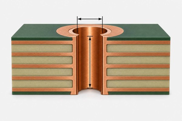
PCB Aspect Ratio is plated-hole depth divided by reference diameter. Calculate it from the actual via span and the fabricator’s diameter convention, then verify the pad, annular ring, plating and tolerances before approving the via.

What Is PCB Aspect Ratio and Why Does It Matter When Choosing Via Size?
PCB Aspect Ratio compares plated-hole depth with hole diameter. A higher PCB Aspect Ratio makes desmear, solution exchange and copper deposition at the barrel center more difficult, increasing the risk of thin copper, voids and thermal-cycle failure.
- Plating: Confirm that the ratio is below the fabricator’s approved limit with allowance for board-thickness and hole-size tolerances.
- Routing: Check whether a larger drill and pad would remove routing channels or reduce plane clearance.
- Via structure: Use blind, buried or microvias only when a shorter span solves a verified density or signal-integrity constraint.
- Complete geometry: Approve the via only when the hole, pad, annular ring, antipad and layer span pass together.
Which Measurements Do You Need Before Calculating PCB Aspect Ratio?
You need two calculation inputs—plated depth and reference diameter—plus the geometry and tolerances required to validate the result. Take them from the released stackup, drill chart and fabrication drawing.
- Depth: Use finished board thickness for through holes, drilled sub-lamination thickness for buried vias, and the actual start-to-stop span for blind vias.
- Diameter: Record nominal drill size and finished-hole size separately; identify which value the fabricator uses for its limit.
- Padstack: Record pad and antipad diameters, required annular ring, and capture/target pads for microvias.
- Tolerances: Include maximum plated depth, minimum permitted reference diameter and drill-position tolerance.
- Process: Identify mechanical drilling, controlled-depth drilling or laser drilling and the applicable supplier limit.
Create one row per via family: start/stop layers, drill method, nominal/maximum depth, nominal/minimum reference diameter, finished-hole requirement, pad diameter and process limit. If “tool size” and “finished hole” are identical without a plating allowance, clarify the data before calculating.
What Is the PCB Aspect Ratio Formula, and How Do You Apply It to Different Via Types?
PCB Aspect Ratio = plated hole depth ÷ reference diameter.
- Mechanical holes: Use the nominal drill-tool diameter unless the fabricator explicitly defines the limit by finished-hole diameter.
- Laser microvias: Use capture-to-target depth and the fabricator-defined diameter measurement point because the hole is tapered.
- Through-hole example: A 1.60 mm board drilled with a 0.25 mm tool gives 1.60 ÷ 0.25 = 6.4:1.
- Buried mechanical-via example: A 0.80 mm drilled sub-lamination with a 0.20 mm tool gives 0.80 ÷ 0.20 = 4:1. Use the drilled sub-lamination thickness, not the final board thickness.
- Laser-microvia example: A 0.075 mm capture-to-target depth divided by a supplier-defined 0.10 mm diameter gives 0.75:1. This is below the IPC-T-50M microvia maximum of 1:1, but the actual diameter convention and production limit still require fabrication approval.
Compare each result with the supplier limit for that drill process and stackup.
Should You Use Drill Size or Finished Hole Size in the Calculation?
Use the diameter specified in the fabricator’s aspect-ratio convention. Drill size and finished-hole size are not interchangeable because barrel copper reduces the opening.
- Mechanical vias: Use nominal drill-tool diameter when the supplier’s capability is defined before plating.
- Finished component holes: Control the finished opening for lead or press-fit fit, but calculate ratio with that value only if the supplier explicitly requires it.
- Laser microvias: Confirm whether the stated diameter is measured at the capture side, target side or after plating.
For component holes, start with the required finished opening and obtain the supplier’s drill allowance. For signal vias, start with an available drill tool and verify the finished range. Show both dimensions in the drill chart and label the ratio reference.
How Do You Calculate the Minimum Via Hole Size for a Given Board Thickness?
Divide drilled depth by the maximum approved ratio to obtain the theoretical minimum reference diameter. Then select an available drill that also meets finished-hole size, plating allowance and tolerance.
Theoretical minimum reference diameter = drilled depth ÷ maximum approved aspect ratio
For a 1.60 mm board limited to 8:1, the theoretical drill is 1.60 ÷ 8 = 0.20 mm. This is not a 0.20 mm finished hole because plating reduces the opening. The BestPCBS capability workbook lists 0.20 mm as the standard minimum finished hole, so the production drill must include plating and process allowance. A 0.25 mm drill gives 6.4:1; confirm its finished range with the fabricator.
For a 0.30 mm partial-depth mechanical via, use 0.30 mm—not total board thickness. For a laser microvia, use supplier-defined depth and diameter. Check the selected tool against the PCB drill size guide and supplier DFM.
What Are the Typical PCB Aspect Ratio Limits for Different Via Types?
Aspect-ratio limits depend on drill method and plated depth. Use these values for screening and obtain supplier approval for the final stackup.
| Via type | Depth used | Practical screening point | Required check |
| Plated through hole | Finished board thickness | 6:1 to 8:1 is a common conservative starting range | Confirm drill convention, plating and board-thickness tolerance |
| Mechanical blind or buried via | Actual connected layer span | Supplier-specific; keep the span as short as the design permits | Confirm sequential lamination and drill access |
| Laser microvia | Dielectric depth between adjacent layers | 1:1 or lower; lower ratios provide more process margin | Confirm target pad, capture pad, stacking and fill requirements |
EBest Circuit lists maximum through-hole PCB Aspect Ratio values of 8:1 standard and 10:1 advanced, with minimum finished holes of 0.20 mm and 0.15 mm respectively. The 10:1 option requires project review.
Treat the maximum as a rejection threshold, not a design target. Near-limit designs require a tolerance and plating review plus confirmation that a larger standard drill cannot provide safer margin. Never apply a through-hole limit to blind, buried, stacked or laser-drilled structures.
How Do Board Thickness, Layer Count and Stackup Affect Via Size?
Board thickness directly raises a through-hole ratio; layer count matters only when it changes thickness, registration or the via span. A 0.20 mm drill gives 6:1 in a 1.20 mm board but 10:1 in a 2.00 mm board.
- Through vias: Use finished board thickness and enlarge the drill if added thickness exceeds the approved ratio.
- Blind vias: Recalculate whenever the stop layer moves.
- Buried vias: Use the drilled sub-lamination thickness, not the final board.
- Microvias: Check each buildup dielectric and its capture/target pad geometry separately.
Freeze the stackup before final padstack approval. Recalculate after changes to finished thickness, dielectric spacing, copper weight or start/stop layers, then recheck pads, antipads and routing clearance.
How Do Pad Diameter, Annular Ring and Hole Tolerance Affect Final Via Size?
A via passes only when enough copper remains around the worst-case hole after diameter and registration tolerances.
Nominal annular ring = (pad diameter − hole diameter) ÷ 2
A 0.60 mm pad around a 0.30 mm hole gives a nominal 0.15 mm ring. Maximum hole size and drill shift reduce the remaining copper, so apply the fabricator’s acceptance method instead of subtracting assumed tolerances.
- Hole enlargement: Increase the pad until the worst-case remaining annular ring meets the fabrication requirement.
- Clearance: Recheck antipads, planes and routing space after changing the padstack.
- Layer review: Verify capture pads on every connected layer and the rule for nonfunctional-pad removal.
- Component holes: Keep press-fit and leaded-hole tolerances separate from ordinary signal vias.
How Do Copper Plating and Reliability Requirements Affect Via Size Selection?
Reliability requirements may require a larger hole than the mathematical minimum because the barrel center is the hardest area to plate uniformly. Thin center-wall copper concentrates strain during assembly and thermal cycling.

- Copper requirement: Define measurable finished barrel copper and the applicable acceptance class.
- Risk factors: Add margin for thick boards, small drills, heavy copper and repeated thermal excursions.
- Evidence: Specify coupon sampling, microsection locations, electrical test and required thermal stress.
- Material system: Consider laminate z-axis expansion, resin system and assembly temperature with the ratio.
A microsection proves only the sampled location. Use it to inspect barrel-center copper, voids and interconnection quality, then combine it with the sampling plan, electrical testing and required thermal qualification. Requalify after a material, thickness or via-geometry change.
When Should You Choose Through-Hole, Blind, Buried or Microvias?
Use the least complex via that meets the required layer connection, routing density and signal-integrity target. Start with through holes; add blind, buried or microvias only when they solve a specific constraint.
- Through hole: Preferred when its pad and antipad fit, inner routing remains open and the unused barrel does not create an unacceptable high-speed stub. Ratio depth is the full board thickness.
- Blind via: Connects an outer layer to selected inner layers, preserving deeper routing channels. Confirm controlled depth, mechanical drill access and sequential-lamination impact.
- Buried via: Connects only internal layers without using outer-layer space. Calculate from the drilled sub-lamination and justify the added lamination and inspection steps.
- Laser microvia: Best for adjacent-layer, fine-pitch HDI escape where a mechanical pad will not fit. Define capture/target pads, staggered or stacked construction, fill and cap requirements.
Before release, check pad/antipad fit, stub length, layer access, lamination cycles, fill/cap needs and inspection cost. Confirm the structure against the PCB via types guide and supplier DFM before routing is frozen.
How Can You Check PCB Aspect Ratio and Via Size During DFM Review?
DFM must calculate the PCB Aspect Ratio for every unique via family—not only the smallest hole—and record a Pass, Revise or Supplier Review disposition.
- Freeze inputs: Use matching revisions of stackup, Gerber/ODB++, NC drill files, fabrication drawing and drill chart; stop if thickness, layer numbers or hole values conflict.
- Group via families: Separate by drill method, start/stop layers, tool diameter, finished-hole requirement, plating status and tolerance.
- Confirm conventions: Record drill and finished diameters separately and define the laser-microvia measurement point.
- Calculate both cases: Nominal ratio uses nominal depth/diameter; conservative ratio uses maximum depth/minimum reference diameter when supplier tolerances are available.
- Check padstack: Verify remaining annular ring, capture/target pads, antipads, copper spacing and solder-mask treatment after any hole change.
- Check process: Identify sequential lamination, fill, copper cap, backdrill, plating, coupons and thermal-stress requirements.
- Close disposition: Pass only when ratio, geometry and process all pass; otherwise revise the design or retain written supplier approval.
Example: 1.60 mm depth ÷ 0.25 mm drill = 6.4:1 nominal. If supplier-defined limits are 1.68 mm maximum depth and 0.24 mm minimum diameter, the conservative value is 7.0:1. Record both values, the applicable limit and disposition; recalculate after any stackup or drill change.
Which Via Sizing Mistakes Increase Cost or Cause Fabrication Defects?
Incomplete drill definitions and calculations made without tolerance margin cause avoidable tooling, lamination and redesign costs.
| Mistake | Likely consequence | Practical correction |
| Using finished hole in one file and drill tool in another | Conflicting ratio, tolerance and quote assumptions | Show both values and identify the calculation convention |
| Calculating blind vias from total board thickness | Incorrect rejection or an unnecessarily large via | Use the actual start-to-stop layer depth |
| Selecting the mathematical minimum without margin | Lower yield and tighter process control | Choose a larger standard drill where routing permits |
| Enlarging the hole but not the pad | Reduced annular ring or breakout | Recalculate pad, clearance and registration margin together |
| Stacking microvias without supplier approval | Extra process steps and reliability risk | Confirm stacking, filling and qualification before layout release |
Correct the geometry before requesting tighter tolerances. Compare a larger drill, shorter span, larger pad and simpler via structure. Blind/buried vias add lamination cost; stacked microvias may add filling, planarization, copper capping and qualification.
What Via Specifications and PCB Files Should You Send for Manufacturing Review?
Send matching-revision fabrication data, drill data, stackup and acceptance requirements.
- Fabrication data: Gerber or ODB++ files with matching revision identifiers.
- Drill data: NC drill files, drill map and a chart separating tool size, finished size, plated status and tolerance.
- Stackup: Finished thickness, materials, copper weights and the depth of every blind or buried span.
- Via construction: Start/stop layers, stacked or staggered arrangement, fill, cap, tent and backdrill requirements.
- Acceptance: Product class, plating requirement, impedance, coupon, microsection and electrical-test needs.
- Commercial context: Prototype and production quantities, forecast, delivery target and any approved alternative.
Add one calculation row per via family: ID, drill method, start/stop layers, depth, nominal tool or microvia diameter, finished-hole requirement/tolerance, pad diameter, fill/cap/tent or backdrill requirement, calculated ratio and capability limit. Label every value as nominal, minimum, maximum or finished.
If DFM changes a drill or layer span, regenerate the affected files. Obtain written approval for accepted via families and exceptions before production release.
FAQs About PCB Aspect Ratio
Q1: Does backdrilling change the original plated-through-hole aspect ratio?
A1: Backdrilling removes an unused barrel section after the through hole has been drilled and plated, so it does not change the original plating challenge. Specify backdrill depth, residual stub and clearance separately.
Q2: Does controlled impedance set the allowable aspect ratio?
A2: No. Controlled impedance governs transmission-line geometry, while the allowable ratio is a hole-manufacturing limit. Via diameter, pad, antipad and stub length can affect impedance and must be modeled separately.
Q3: Do non-plated holes have a PCB via aspect ratio?
A3: A depth-to-diameter ratio can be calculated, but the plating-related via limit does not apply in the same way to an NPTH. Mechanical drilling capability, positional tolerance and tool access still need review.
Q4: How is aspect ratio handled for plated slots?
A4: Use the plated depth and the slot’s controlling narrow dimension, then confirm the supplier’s routing and plating rule. End radius, slot width, tolerance and copper coverage also affect approval.
Q5: Does via filling change the calculated ratio?
A5: No. Filling occurs after the hole is formed and plated, so it does not change the original depth-to-diameter calculation. It does add material, process and planarization requirements that need separate DFM checks.
Q6: Should press-fit component holes use the same diameter strategy as signal vias?
A6: No. Press-fit holes are sized around the component pin and finished-hole tolerance, not routing density. Confirm the compliant-pin specification, plating build and insertion-force requirements before selecting the drill.
Q7: Does a lower ratio always improve electrical performance?
A7: Not necessarily. A lower ratio generally improves plating access, but electrical behavior depends on via length, diameter, pad and antipad geometry, stub length and return path. Evaluate high-speed performance separately.
Q8: Can aspect ratio alone predict conductive anodic filament risk?
A8: No. CAF risk also depends on material system, spacing, moisture, voltage, drilling damage and processing cleanliness. Treat it as a separate material and reliability assessment.
Q9: Does via tenting affect PCB Aspect Ratio?
A9: No. Solder-mask tenting covers the via opening but does not change the drilled depth or diameter. Tenting may affect assembly protection, outgassing and inspection, so specify it independently.
Q10: Can aspect ratio determine how much current a via carries?
A10: No. Current capacity depends mainly on finished barrel copper, hole geometry, temperature rise and the connected copper features. Aspect ratio helps assess manufacturability but cannot replace an electrical and thermal calculation.
Need a project-specific via check? Send your Gerber or ODB++ package, NC drill files, controlled stackup, target quantity and via table to sales@bestpcbs.com. EBest Circuit can review the proposed PCB Aspect Ratio, hole convention, annular ring and via structure before quotation.