Artificial intelligence in PCB assembly optimization is becoming more practical as SMT lines generate increasing amounts of production and inspection data. SPI, placement machines, reflow ovens, AOI, X-ray inspection, testing, and traceability systems all provide information that can be used to identify process patterns. AI helps connect these data points, allowing engineers to detect abnormalities earlier and investigate why defects occur rather than only where they are found.
For PCB assembly buyers, the real value is better process control, inspection, and yield—not AI for its own sake. EBest Circuit supports PCB fabrication, PCBA assembly, and box-build projects from prototypes to volume production. If your project has demanding assembly, inspection, testing, or traceability requirements, send your Gerber files, BOM, and assembly requirements to sales@bestpcbs.com for an engineering review.
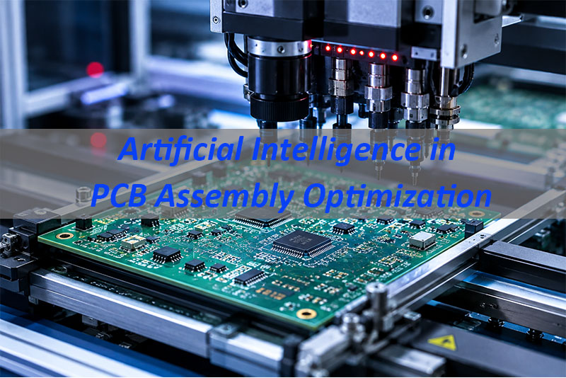
What Is AI in PCB Assembly?
AI in PCB assembly refers to the use of machine learning, computer vision, pattern recognition, and data analytics to support manufacturing decisions.
Traditional PCB assembly relies on machine programs, process limits, SPC, inspection rules, and engineering experience. AI adds another layer by analyzing larger volumes of production data and identifying relationships between different process variables.
For example, an AOI defect may be linked to solder paste volume, placement offset, component geometry, or reflow conditions. Instead of examining each stage separately, AI can help correlate these records.
Typical applications include:
- defect recognition and classification;
- AOI and X-ray image analysis;
- SMT process optimization;
- yield analysis;
- process drift detection;
- root-cause analysis.
AI is therefore most useful when it works alongside established process controls and manufacturing engineering rather than replacing them.
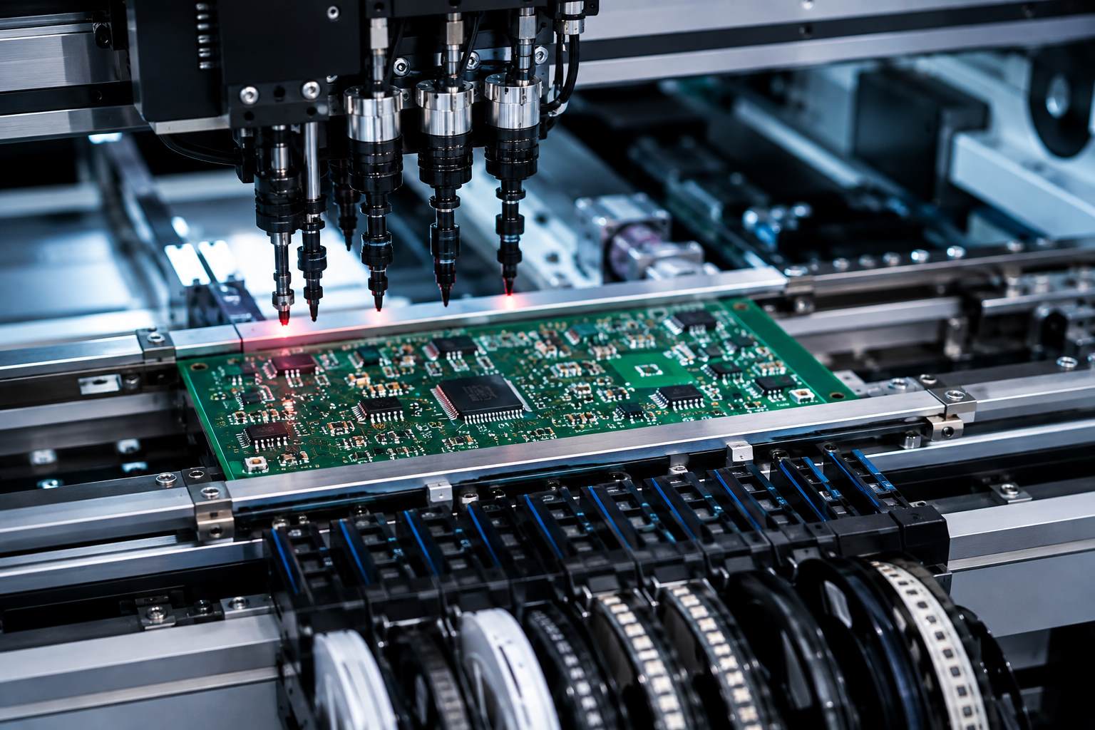
How Is AI Used in PCB Assembly?
AI can be applied across several stages of PCB assembly because each stage produces different types of manufacturing data.
Typical sources include:
- SPI: solder paste height, area, volume, and offset;
- Placement: coordinates, corrections, feeder and nozzle data;
- Reflow: temperature profiles, zone settings, and conveyor speed;
- Inspection: AOI images, X-ray images, and defect records;
- Testing: ICT, functional test, and failure results;
- Traceability: PCB serial numbers, material lots, machines, and production history.
The key advantage comes from connecting these records.
If AOI repeatedly finds insufficient solder on the same package, engineers can compare those failures with earlier SPI, placement, and reflow data. This shifts the investigation from where a defect was detected toward which upstream condition may have contributed to it.
That cross-process visibility is one of the main ways AI can support PCB assembly optimization.
How Does AI Optimize the SMT Assembly Process?
AI can help engineers analyze relationships between solder paste printing, placement, reflow, and downstream inspection results.
Solder Paste Printing
- SPI data can reveal changes in paste volume, height, area, or offset. When these measurements are compared with later defects, engineers can identify patterns that deserve attention.
Component Placement
- Placement data can reveal repeated corrections associated with a particular component, feeder, nozzle, or board location. Instead of treating each adjustment as an isolated event, historical data can show whether the pattern is becoming systematic.
Reflow Soldering
- AI can compare production results with variables such as zone temperature, conveyor speed, package size, and board characteristics. This can help engineers narrow down process combinations associated with recurring soldering problems.
The objective is not to replace thermal profiling or process engineering. It is to use historical production data more effectively so engineers can investigate potential causes and make process adjustments with better evidence.
How Does AI Improve PCB Assembly Inspection?
Inspection is one of the most practical areas for AI in PCB assembly because modern inspection equipment already generates large amounts of image and measurement data.
AOI
AOI may inspect conditions such as:
- missing or misplaced components;
- polarity errors;
- solder bridges;
- insufficient solder;
- lifted leads;
- abnormal solder-joint appearance.
Machine-learning models can help distinguish actual defects from acceptable process variation. This is particularly useful when conventional inspection rules generate excessive false calls.
X-Ray Inspection
AI can also support X-ray analysis for hidden solder joints under BGA, QFN, and other bottom-terminated packages. Typical inspection targets include voiding, bridging, insufficient solder, alignment issues, and hidden joint abnormalities.
The practical benefit is not simply detecting more features. Better classification can reduce unnecessary review while making inspection results more useful for upstream process correction.
How Does AI Detect PCB Assembly Defects?
AI-based defect detection commonly uses computer vision or measurement data to recognize patterns associated with known assembly defects.
Depending on the inspection method, these may include:
- missing components;
- component shift;
- reversed polarity;
- tombstoning;
- solder bridges;
- insufficient solder;
- lifted leads;
- hidden solder-joint abnormalities.
A trained model can compare new inspection data with previously classified examples and estimate whether a condition represents normal variation or a genuine defect.
AI can also help group repeated failures. If the same defect appears on one reference designator, package type, component lot, or production line, the pattern becomes easier to identify.
However, reliable detection still depends on representative training data and consistent defect classification. AI can improve the speed of analysis, but inspection criteria and engineering validation remain essential.
How Does AI Improve PCB Assembly Yield?
AI can support PCB assembly yield improvement by connecting defect results with the process conditions that occurred earlier in production.
Instead of looking only at the final yield percentage, engineers can compare failures with:
- SPI measurements;
- placement corrections;
- reflow conditions;
- AOI or X-ray results;
- component lots;
- repair records;
- electrical test failures.
This can make recurring failure patterns easier to identify.
First-Pass Yield
First-pass yield is particularly useful because repeated inspection, repair, and retesting add time and handling to the assembly process. AI-based analysis can help engineers focus on process variables that show a strong relationship with recurring defects.
Root-Cause Analysis
Connected production data can also reduce the time needed to trace a defect back through earlier processes.
For example:
AOI detects a solder defect → SPI history shows abnormal paste variation → engineers inspect stencil or printing conditions.
The practical goal is straightforward: identify problems earlier and shorten the path from defect detection to corrective action.
What Data Does AI Need for PCB Assembly Optimization?
Useful AI analysis depends more on data quality and traceability than simply collecting a large quantity of data.
Common inputs include:
- SPI measurements;
- placement and correction records;
- reflow parameters;
- AOI and X-ray results;
- defect classifications;
- rework records;
- ICT and functional test results;
- PCB serial numbers;
- component lot information;
- machine and production timestamps.
Traceability is especially important. If a failed board cannot be connected to its earlier manufacturing history, root-cause analysis becomes much harder.
Consistent labeling also matters. Similar defects should not be recorded under several unrelated names if the data will later be used for model training or statistical analysis.
For many manufacturers, improving data structure is therefore an important first step before introducing more advanced AI tools. Good manufacturing data gives both AI systems and engineers a stronger basis for decision-making.
What Are the Challenges of Using AI in PCB Assembly?
One challenge is high-mix production. An EMS factory may assemble many PCB designs with different packages, materials, volumes, and inspection requirements. A model that performs well on one product may require adjustment for another.
Other practical issues include:
- inconsistent data formats between equipment;
- limited historical data for prototypes or low-volume builds;
- false positives and missed defects;
- process changes after material or equipment adjustments;
- inconsistent defect labeling.
AI also identifies correlations, which are not always the same as root causes. A change in defect rate may coincide with a reflow adjustment, for example, while the actual cause is related to solder paste, PCB design, component condition, or another variable.
For this reason, AI works best as an engineering support tool.
The most reliable approach combines production data, AI analysis, established process controls, and manufacturing engineering judgment.
FAQs About Artificial Intelligence in PCB Assembly Optimization
Can AI completely automate PCB assembly optimization?
Not in most production environments. AI can assist with inspection, process analysis, prediction, and troubleshooting, while engineers still validate process changes and product-specific requirements.
What PCB assembly data can AI analyze?
AI can analyze SPI measurements, placement data, reflow records, AOI and X-ray images, defect history, rework records, traceability information, and electrical test results.
Can AI reduce PCB assembly defects?
AI can identify patterns associated with recurring defects and help engineers detect abnormal process trends earlier. Actual defect reduction comes from applying appropriate corrective actions based on those findings.
Is AI suitable for low-volume PCB assembly?
Yes, although the approach may differ from mass production. Low-volume projects may have less product-specific historical data, so generalized inspection models, cross-product data, and engineering rules become more important.
How is AI different from traditional PCB assembly process control?
Traditional process control relies on defined limits, machine settings, SPC, inspection criteria, and engineering experience. AI adds pattern recognition and predictive analysis across larger datasets. In practice, the two approaches complement each other.
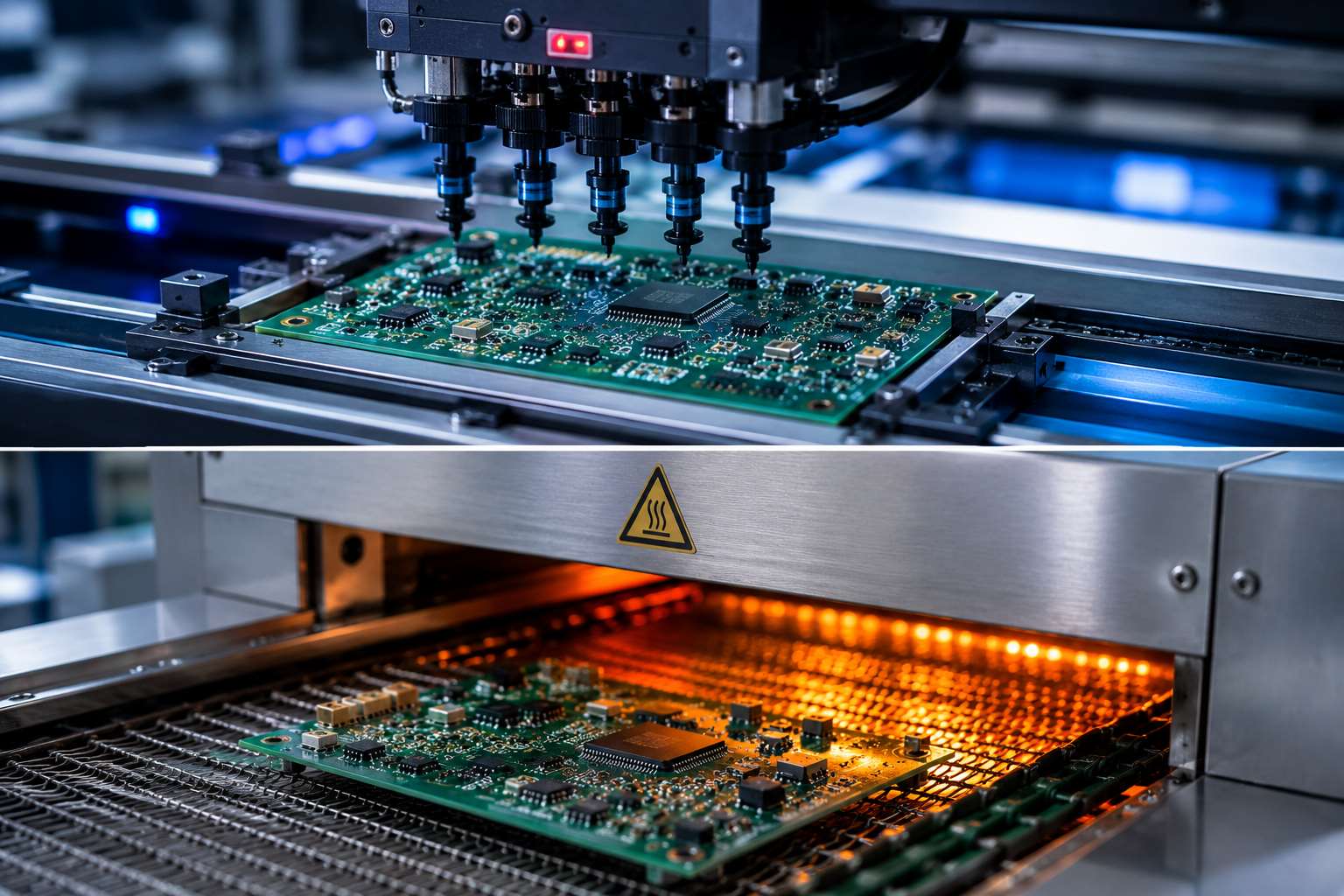
If you are developing a PCB or PCBA project and need support with assembly process control, inspection, testing, or traceability, EBest Circuit can review your manufacturing files before production. Send your Gerber files, BOM, assembly drawings, test requirements, and expected quantity to sales@bestpcbs.com so our team can evaluate the project and prepare an appropriate manufacturing and quotation plan.