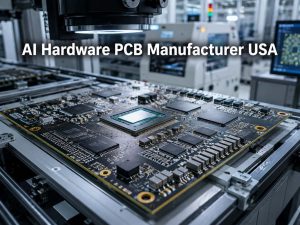
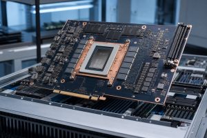
AI server power board is an emerging term for a board that converts or distributes high-density power inside an AI server, compute tray, or closely related power assembly. It is not automatically the same as a complete server PSU, rack PDU, motherboard, or power shelf. The exact meaning depends on where the board sits in the power chain and which voltage conversion or distribution function it performs.
EBest Circuit supports high-current PCB fabrication, component sourcing, PCBA, inspection, and agreed board-level testing for customer-approved power electronics. If you are preparing a high-power DC-DC board or power delivery board for production, send the released PCB files, BOM, mechanical information, and test requirements to sales@bestpcbs.com for a manufacturing review.
What Is an AI Server Power Board?
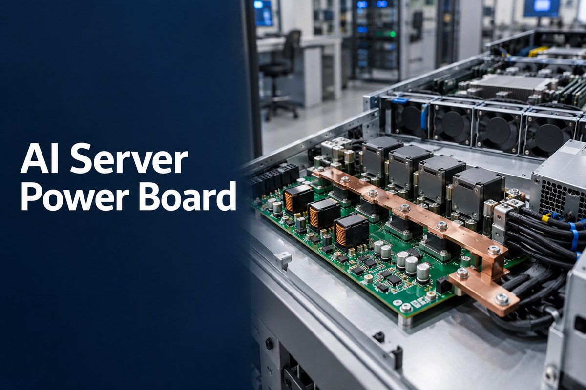
An AI server power board is a PCB or PCBA that converts or distributes power near the computing hardware. Depending on the architecture, it may carry an intermediate bus voltage, step that voltage down, or connect a power shelf to GPU, accelerator, CPU, and memory loads.
The term needs context because several assemblies in a server handle power:
- a rack PDU distributes facility power to equipment.
- a power shelf contains multiple power supplies and may provide redundancy.
- a server power supply converts AC or high-voltage DC into an intermediate DC output.
- a power delivery board performs a board-level conversion or distribution function closer to the load.
- voltage regulator modules provide the final low-voltage, high-current rails used by processors and memory.
An AI server power board may therefore be a large distribution board, a compact high-ratio DC-DC board, or part of a tray-level power assembly. Its identity comes from its electrical function and position—not simply from being a PCB installed in an AI server.
Where Does a Power Delivery Board Fit in the AI Server Power Architecture?
A power delivery board normally sits between the server’s intermediate DC supply and the final point-of-load regulators. Power reaches an accelerator through a chain such as:
Facility input → rack distribution → power shelf or PSU → intermediate DC bus → power delivery board → point-of-load regulation → GPU or accelerator
Moving conversion closer to the compute tray shortens high-current, low-voltage paths. Because conductor loss rises with the square of current, carrying power upstream at a higher voltage can reduce current and distribution loss.
The board may also provide input protection, controlled startup, isolation, voltage conversion, current sharing, sensing, and connections to busbars or cable assemblies. These functions vary by platform. A board described only as an “AI server power board” still needs an input range, output range, rated power, isolation requirement, cooling method, and mechanical envelope before it can be treated as a defined product.
AI Server Power Supply vs Power Delivery Board: What Is the Difference?
An AI server power supply usually creates the intermediate DC supply. A power delivery board converts or distributes that power closer to the computing load. A point-of-load regulator then produces the final processor rails.
| Assembly | Main role | Usual location |
| Server PSU | Creates an intermediate DC supply | Power shelf or server input |
| Power delivery board | Converts or distributes power near the load | Compute tray or accelerator assembly |
| Point-of-load regulator | Produces final processor rails | Compute board |
The distinction affects manufacturing. A complete PSU usually includes an enclosure, fan or cold plate, safety spacing, input/output connectors, and its own control electronics. A power delivery board may instead depend on the server chassis for cooling, insulation coordination, busbar support, and mechanical protection.
Calling every power-related assembly a PSU hides these differences. The PCB stackup, copper weight, connector system, cooling interface, assembly sequence, and test fixture all depend on the board’s actual place in the architecture.
Why Is 800 VDC Power Delivery Moving Closer to the Compute Tray?
It is moving closer to the compute tray because high voltage reduces upstream current, while local conversion limits the distance that very high low-voltage current must travel. AI accelerators have increased rack power demand and concentrated that demand into smaller spaces. Transporting very high power at 48 V or another low intermediate voltage requires large currents, heavier conductors, and more demanding connections.
An 800 VDC architecture carries a given amount of power at much lower current than a 48 V path. For example, ignoring conversion losses, 20 kW corresponds to about 25 A at 800 V but more than 416 A at 48 V. The lower upstream current can reduce distribution loss and conductor mass.
The difficult conversion does not disappear; it moves. A board located near the compute tray must step the high-voltage bus down efficiently while fitting within strict height, cooling, creepage, clearance, and service requirements. The architecture therefore trades a heavy low-voltage distribution path for a demanding high-ratio conversion stage closer to the load.
This is a developing architecture rather than a universal AI-server standard. Many current systems still use established AC-input PSUs, 48 V power shelves, or other intermediate-bus arrangements. An 800 VDC board should be described as a platform-specific solution, not as a required feature of every AI server.
How Does an 800 V-to-6 V DC-DC Power Delivery Board Work?
An 800 V-to-6 V board switches the high-voltage input, transfers energy through a high-ratio conversion stage, and delivers a regulated low-voltage, high-current output. Its exact topology belongs to the approved electrical design, but the functional path normally contains five recognizable sections.
High-voltage input: Protection, filtering, controlled startup, and bus sensing prepare the incoming DC supply for conversion. High-voltage spacing and transient conditions affect both the schematic and the physical PCB.
Switching stage: Power semiconductors switch the input at high frequency so energy can be transferred efficiently. Fast switching reduces the size of some magnetic components but makes parasitic inductance, gate-loop geometry, ringing, and EMI more important.
Isolation and voltage transformation: Where isolation is required, high-frequency magnetics provide the safety barrier and most of the voltage transformation. The winding structure, insulation system, leakage inductance, and PCB connection geometry influence both loss and voltage stress.
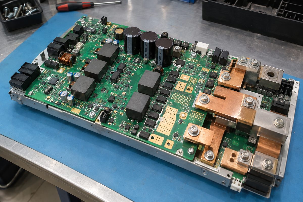
Secondary conversion: Low-voltage switching devices or synchronous rectifiers handle very high current. At this stage, milliohms matter. Copper paths, joints, terminals, and busbar interfaces can each become a meaningful heat source.
Output distribution and control: Current sensing, voltage feedback, protection, current sharing, and communication support stable operation. The 6 V output may then feed additional point-of-load stages that produce the final processor rails.
The board is therefore not simply a thick-copper PCB. Electrical design, magnetics, switching behavior, insulation, thermal interfaces, and mechanical integration must work as one assembly.
How Do Copper, Vias, and Busbars Carry High Current Without Excess Heat?
Copper planes provide broad current paths, via arrays connect those paths through the stackup, and busbars carry current beyond practical PCB-copper limits. They control heat only when the complete path has low resistance. Thicker copper cannot compensate for a narrow neck, insufficient via area, small connector contact, or resistive joint.
Copper planes: Wide, short planes reduce resistance and spread heat. Heavy copper can increase current capacity, but it also affects etching, minimum spacing, laminate fill, board thickness, and copper balance.
Parallel layers: Several copper layers can share current when the transitions between them are adequately connected. Current distribution is not automatically equal; entry points, via placement, geometry, and nearby magnetic fields influence which layers carry the greatest load.
Via arrays: Vias move current between layers and conduct heat through the board. Their useful capacity depends on finished hole size, plating thickness, quantity, pitch, temperature rise, and how current enters the array. A large number of poorly positioned vias can still create local crowding.
Busbars and terminals: Busbars can carry current with lower resistance and greater mechanical stiffness than PCB copper alone. The interface is often the critical area. Hole tolerances, surface flatness, fastener loading, plating, solder volume, and contact resistance affect the finished connection.
Joints and component pads: Low-voltage output stages may use large leadless packages, clips, or high-current connectors. Voids, insufficient solder, uneven coplanarity, and localized copper imbalance can raise resistance and temperature even when the nominal PCB copper is adequate.
Thermal imaging and voltage-drop measurements are valuable because they reveal the complete path. A board can pass continuity testing and still contain a small resistive region that becomes visible only under load.
What Do GaN Power Stages Change in PCB Layout and Assembly?
GaN power stages make loop inductance, gate routing, hidden solder joints, cleanliness, and thermal interfaces more critical. The devices can switch rapidly and reduce some switching losses, but their speed makes the physical interconnect part of the circuit behavior.
The switching loop must be compact because stray inductance can produce overshoot, ringing, EMI, and additional device stress. Gate-drive paths require controlled geometry and a short return path. Power and control grounds may need carefully managed connections so that high di/dt current does not disturb sensing or control signals.
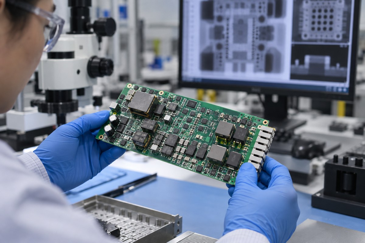
Package style changes assembly requirements. Bottom-terminated GaN packages can hide solder joints from normal optical inspection. Pad geometry, stencil apertures, solder volume, placement accuracy, reflow profile, and void control influence both electrical and thermal performance. X-ray can examine hidden-joint coverage and major voiding where the package and acceptance criteria make that inspection meaningful.
Fast switching also increases the importance of cleanliness and spacing. Residue near high-field regions, damaged solder mask, copper-edge variation, and uncontrolled rework can reduce manufacturing margin. These issues are best managed through the released fabrication and assembly data rather than corrected after the board has already entered volume production.
GaN does not remove the need for magnetics, protection, thermal design, or validation. It changes where loss occurs and how sensitive the converter is to layout, assembly variation, and parasitic elements.
How Are Thermal Interfaces and Cooling Integrated Around the Board?
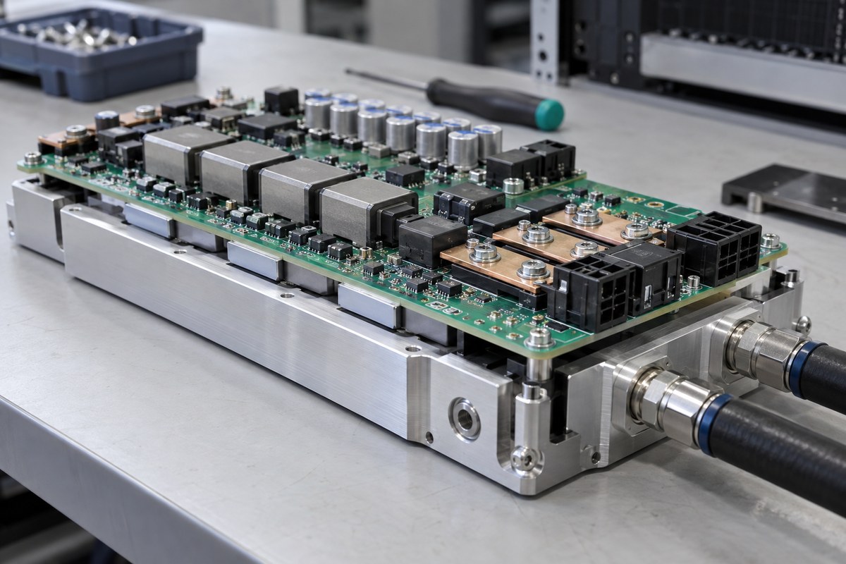
Cooling is integrated by building a continuous thermal path from the power devices through the package, PCB or spreader, interface material, and heat sink or cold plate. Heat can also leave through copper planes, thermal vias, solder joints, busbars, and the PCB edge. The dominant path depends on the package and server cooling architecture.
Air-cooled assemblies may use heat sinks and directed airflow, but dense AI hardware increasingly places strict limits on airflow resistance and component height. Conduction-cooled or liquid-cooled assemblies can move heat through a baseplate or cold plate, provided that the thermal interface remains flat, compressed, and electrically safe.
A practical thermal stack can include:
- the semiconductor junction and package.
- solder or die-side thermal interface.
- PCB copper and thermal vias.
- a gap pad, phase-change material, or other interface material.
- a heat spreader, heat sink, chassis, or liquid cold plate.
Each interface adds thermal resistance. Excess bond-line thickness, board bow, uneven component height, voids, insufficient contact pressure, and tolerance accumulation can prevent the cooling hardware from performing as expected.
Mechanical and thermal design therefore affect PCB production. Copper balance influences flatness. Component height controls interface compression. Keep-out areas may be needed for cold-plate features and fasteners. Heavy magnetic parts and busbars may require additional support so that their mass does not strain solder joints during transport or service.
Which Board-Level Tests Reveal Loss, Temperature Rise, and Load-Step Problems?
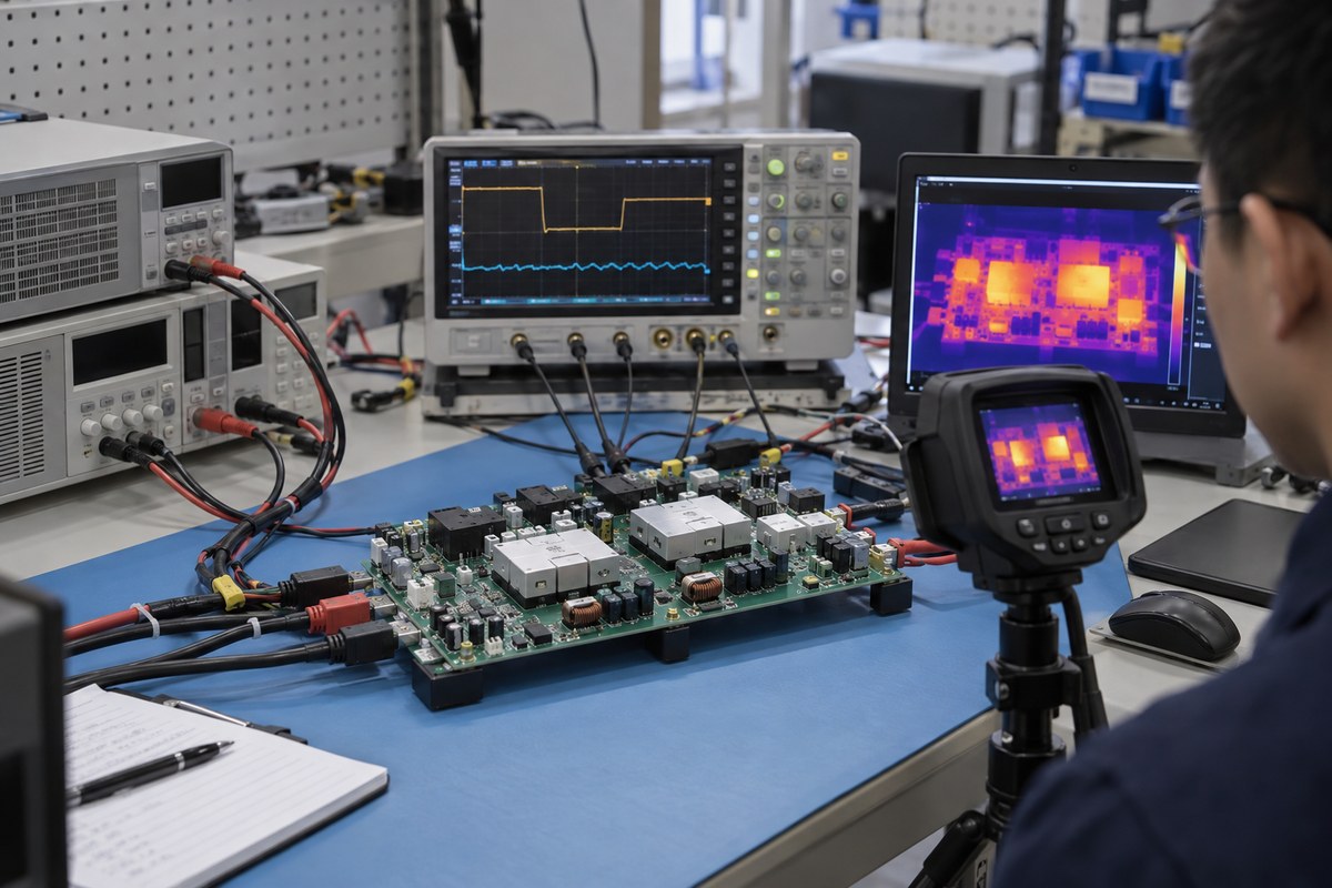
Efficiency testing reveals conversion loss, thermal measurements reveal hotspots, and load-step testing reveals transient response. Assembly inspection and preliminary electrical checks are still needed because those three performance tests do not identify every manufacturing defect.
| Test | Primary finding |
| AOI or visual inspection | Visible assembly defects |
| X-ray inspection | Hidden joints and major voiding |
| Continuity and resistance | Opens, shorts, and resistive paths |
| Controlled power-up | Startup and basic regulation |
| Efficiency measurement | Conversion loss |
| Thermal measurement | Local temperature rise |
| Load-step testing | Transient deviation and recovery |
| Insulation testing | Specified insulation integrity |
Test conditions matter as much as the test name. Input voltage, load level, dwell time, airflow or cold-plate condition, sensor position, measurement bandwidth, and acceptance limits determine what the result means.
Board-level testing can verify the manufactured assembly against an agreed specification. Rack-level power sharing, accelerator workload transients, firmware interaction, system cooling, regulatory compliance, and field redundancy still require validation in the intended server platform.
How Can EBest Circuit Support High-Power DC-DC Board Production?
EBest Circuit can turn a customer-approved high-power DC-DC design into a controlled PCB and PCBA production process. Support can extend from manufacturability review through fabrication, sourcing, assembly, inspection, and agreed board-level testing.
Production support includes:
- stackup, copper, spacing, hole, and copper-balance DFM.
- multilayer and heavy-copper PCB fabrication.
- controlled-BOM component sourcing.
- power-device, magnetic-component, and connector assembly.
- reflow, selective soldering, press-fit, and approved special processes.
- AOI, X-ray, electrical inspection, cleanliness control, and traceability.
- customer-defined fixtures and agreed board-level testing.
High-voltage spacing, output-current paths, busbar interfaces, cooling surfaces, and test access deserve attention before release because they connect several manufacturing processes. A change that appears small in one file can affect PCB fabrication, stencil design, assembly order, fixture access, or final inspection.
EBest Circuit does not replace the customer’s power-topology, magnetics, firmware, mechanical, safety, or server-system engineering. Its role is to turn the released product definition into a controlled PCB and PCBA process, identify manufacturing conflicts, and provide agreed production evidence.
AI Server Power Board FAQs
Is an AI server power board the same as a server motherboard?
No. A server motherboard carries processors, memory, high-speed interfaces, management circuits, and local regulators. A power board is primarily responsible for defined power conversion or distribution. Some functions can share one assembly, but the terms are not interchangeable.
Does every AI server use 800 VDC power delivery?
No. Many systems use AC-input PSUs, 48 V shelves, or other intermediate-bus architectures. The 800 VDC approach is an emerging option for reducing upstream current in very high-power systems, not a universal requirement.
Why can a 6 V output still be difficult to manufacture?
Low voltage at high power means very high current. Small resistance in copper transitions, solder joints, terminals, busbars, or connectors can create significant loss and heat. The board must control the complete current path, not only the nominal copper thickness.
Are heavy-copper layers enough for a high-current power board?
Not by themselves. Heavy copper helps reduce resistance, but via transitions, narrow geometries, connector contacts, component pads, busbar joints, and cooling interfaces may still limit the assembly.
What information defines a manufacturable power board project?
The released package normally includes PCB fabrication data, stackup and copper requirements, schematic, controlled BOM, assembly drawings, mechanical and cooling constraints, high-voltage requirements, and board-level test conditions. Together, these files define what must be built and how conformity will be evaluated.
EBest Circuit can review the manufacturing package for your AI server power board and support PCB fabrication, PCBA, inspection, and agreed testing. Send the released project files and production requirements to sales@bestpcbs.com to discuss the next build.