Advanced HDI PCBs become necessary when dense accelerator I/O, fast board-level links, multiple power rails, and cooling hardware compete for the same board area. Fine-line routing, laser-drilled microvias, filled via-in-pad, and selective build-up layers create escape and transition paths that conventional through-hole vias can block.
That pressure is rising in 2026. NVIDIA Rubin, AMD Helios, and new 102.4 Tbps switch silicon show AI systems moving toward more accelerator bandwidth, larger scale-up domains, denser networking, and tighter power-and-cooling integration. At board level, the practical result is more difficult package breakout, more high-speed lanes, heavier power distribution, and less room to solve them.
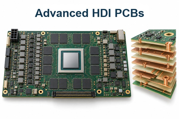
Why Does AI Computing Hardware Need Advanced HDI PCBs?
AI hardware needs advanced HDI when the package map and board outline leave too few routing channels for ordinary through-hole construction. The important gains are specific:
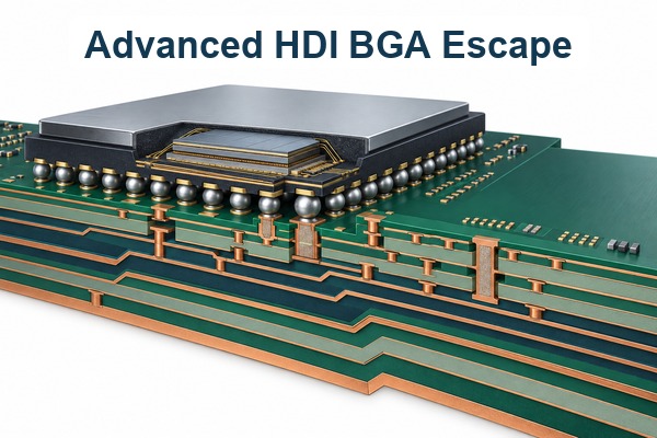
- Dense BGA escape: Blind microvias move power, ground, control, and high-speed signals away from fine-pitch accelerator or switch packages without reserving a through-hole barrel on every layer.
- More usable routing channels: Smaller pads and layer-specific vias leave inner-layer space for differential pairs, clocks, control buses, and power connections.
- Shorter vertical transitions: A microvia can reach the required reference or signal layer without the long unused barrel of a full-depth via.
- Local power access: Via-in-pad and short power-ground transitions help connect dense decoupling and nearby regulators to high-current devices with less interconnect inductance.
- Room for the rest of the system: Routing density preserves surface area for retimers, connectors, stiffeners, cold-plate hardware, test points, and service clearances.
A low-speed management board or power-only board may not need this construction. The trigger is a verified routing, signal, power, or space constraint on the actual board.
Where Are Advanced HDI PCBs Used in AI Computing Hardware?
Advanced HDI is most useful on boards where fine-pitch packages and dense local interconnects occupy the same limited area:
- GPU and AI accelerator cards: Microvias and via-in-pad help escape large accelerator packages, memory-adjacent board interfaces, retimers, clocks, and dense local power connections.
- Accelerator modules and baseboards: High connector counts, scale-up links, switch devices, and management circuits compete for routing and reference-plane space.
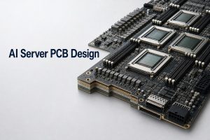
- AI server PCBs and motherboards: Selective HDI can relieve congestion around CPUs, high-speed I/O hubs, PCIe or CXL devices, NICs, and module connectors without forcing advanced rules across the whole board.
- AI network and switch boards: Very large switch ASICs, dense SerDes fan-out, retimers, and pluggable-module connectors create concentrated breakout and transition problems.
- Edge AI compute modules: A small outline must accommodate an AI SoC, memory, PMICs, cameras, storage, sensors, radios, and external I/O, making area efficiency the main driver.
These boards can sit in the same AI system and still require different constructions. An accelerator module may need local high-density build-up, while a long-channel switch board may depend more heavily on low-loss material, backdrilling, and connector-launch control.
How Does Advanced HDI Support GPU and AI Accelerator Boards?
The main job is package breakout. Large GPU, ASIC, and FPGA packages bring thousands of power, ground, clock, control, and high-speed connections into a compact footprint. Conventional capture pads and antipads can close routing channels before those connections reach usable signal and plane layers.
- Blind microvias open escape paths by connecting only the layers needed around the package.
- A filled and capped via-in-pad structure removes the dog-bone penalty where the land pattern leaves no room for a separate fan-out via.
- Selective build-up keeps aggressive geometry local to the accelerator, retimer, or module-connector region instead of applying it to every route.
- Short local transitions reduce congestion between the accelerator and nearby switches, retimers, NICs, CPUs, clocks, and power stages.
The safest design uses the coarsest feature that still closes the breakout. Finer lines, smaller pads, and more stacked microvia levels increase registration, plating, planarization, inspection, and yield demands.
Why Do AI Accelerator Boards Use High-Layer-Count HDI Stackups?
AI accelerator boards push layer counts higher because package breakout, high-speed channels, continuous reference planes, multiple power rails, and connector fan-out all need separate space in the same cross-section. Combining high layer count with selective HDI lets the board assign each constraint to a controlled part of the stack.
- Breakout and build-up layers move dense package connections out of the BGA field before the routes spread across the board.
- High-speed signal layers carry PCIe, scale-up, network, clock, and control paths beside stable reference planes.
- Reference planes give fast signals a continuous return path and reduce coupling between unrelated channel groups.
- Power-distribution layers connect regulators, planes, and decoupling to high-current loads while keeping loop inductance under control.
- Connector and long-channel layers reserve cleaner routing corridors for paths that cannot tolerate repeated layer changes or plane discontinuities.
This is why a high-multilayer HDI PCB can be useful in an accelerator or baseboard: it separates jobs that would otherwise fight for the same routing space. The final layer count should come from the completed escape study, channel plan, PDN model, board thickness, and fabricator review.
How Does Advanced HDI Support High-Speed Interconnects in AI Hardware?
Advanced HDI supports high-speed board links by controlling how signals leave dense packages and reach a continuous routing layer.
- Shorter via barrels reduce unused-stub effects on local transitions where a blind microvia can replace a full-depth plated through hole.
- More escape channels reduce route detours, helping differential pairs reach retimers, switches, CPUs, NICs, or module connectors without unnecessary length.
- Closer reference access improves return-path continuity when the via transition includes the required ground stitching and keeps plane openings under control.
- Selective transitions preserve long-channel options: the dense breakout can use HDI while longer routes use low-loss material, controlled impedance, and backdrilled through vias where those choices provide better margin.
HBM bandwidth is evidence of rising compute density, but HBM traffic between the GPU die and memory stacks stays inside the package and package substrate. The host PCB carries package or module I/O such as scale-up links, PCIe, networking, clocks, control, power, and connector transitions. Simulation should model the channel the PCB actually owns.
Why Do AI Network and Switch Boards Need High-Density Interconnects?
AI switch boards concentrate an unusually large number of SerDes lanes around one switch ASIC. Broadcom announced in March 2026 that Tomahawk 6 was shipping in production volume with 102.4 Tbps switching capacity and support for 100G and 200G SerDes. That scale increases the number of package escapes, reference transitions, retimer connections, and front-panel links a board must organize.
- ASIC breakout is the local HDI problem: fine-pitch balls and a large lane count require many short, controlled escapes close to the switch package.
- Pluggable optics create a connector-density problem: OSFP or similar cages, management devices, power, and thermal clearances compete for the board edge.
- Long routes remain a channel problem: low-loss laminate, trace geometry, connector launches, backdrilling, and return-path design may matter more than microvias once the signal leaves the congested ASIC region.
- Retimers change the partition: placing them near the ASIC or front panel trades routing distance against power density, cooling access, and additional BGA escape.
The design decision is regional. Use advanced HDI where it clears the switch or connector breakout, then select the long-channel construction from the measured insertion-loss, crosstalk, and via-stub budget.
How Does Advanced HDI Support Compact Edge AI Modules?
Edge AI modules use HDI primarily to fit more functions into a fixed, often irregular outline. A single board may combine an AI SoC, memory, PMICs, storage, camera inputs, sensors, radios, USB, Ethernet, and board-to-board connectors.
- Via-in-pad releases component area around fine-pitch SoCs, memories, and PMICs.
- Blind microvias protect inner-layer routing space that a field of through holes would consume.
- Short fan-out supports compact high-speed interfaces between the processor, memory, storage, cameras, and communications devices.
- Selective build-up controls cost by limiting the most demanding rules to dense device regions.
- Smaller transition fields leave room for mechanical needs such as shields, antennas, mounting holes, thermal interfaces, and sealed-enclosure clearances.
Compact does not automatically mean advanced HDI. A board with relaxed pitch, few high-speed interfaces, and enough area may meet its targets with standard multilayer construction. An escape study should show blocked routes or excessive board area before the HDI stack is approved.
How Does Advanced HDI Affect Power and Thermal Design Around AI Accelerators?
Advanced HDI changes power and thermal design by concentrating copper and components while freeing some surface area for regulators and cooling hardware.
- Power delivery: Short via-in-pad and microvia connections can reduce the inductive path between package lands, decoupling, and nearby power or ground planes.
- Regulator placement: Denser breakout may create usable surface area for multiphase stages, inductors, bulk capacitance, current sensing, and control circuits close to the load.
- Heat spreading: Copper planes and via fields alter lateral and vertical heat flow, so conductor losses and component heat must be solved with the real copper distribution.
- Warpage and stress: Uneven copper, multiple build-up layers, large packages, stiffeners, and cold-plate fasteners can produce local bending or interface stress during lamination, reflow, and service.
- Cooling clearances: Cold plates, retention hardware, liquid manifolds, airflow paths, and service access impose keep-outs that reduce the routing area HDI is trying to recover.
- Qualification: Thermal cycling, assembly exposure, cross-sections, resistance monitoring, and representative coupons must match the released microvia structure and material set.
The board should be reviewed with the same stackup in the signal, power, thermal, mechanical, and fabrication models. A routing solution that closes electrically but moves copper or fasteners into the wrong thermal-mechanical condition is not ready for production.
What Do 2026 AI Hardware Platforms Reveal About Future PCB Requirements?
Three 2026 announcements show where board-level pressure is increasing:
- NVIDIA Rubin: NVIDIA lists up to 22 TB/s of HBM4 bandwidth per GPU, 3,600 GB/s of NVLink 6 scale-up bandwidth, PCIe Gen 6 host connectivity, and a rack architecture that integrates compute, networking, liquid cooling, and power controls in its Rubin architecture disclosure. For PCB teams, the relevant pressure is dense module I/O, switch and retimer fan-out, power delivery, and cooling-constrained placement.
- AMD Helios: AMD describes Helios as a rack-scale system combining Instinct MI455X GPUs, EPYC CPUs, Pensando networking, and ROCm software. The board-level implication is tighter co-design among accelerator modules, baseboards, host processors, network fabrics, power shelves, and serviceable trays.
- Broadcom Tomahawk 6: A 102.4 Tbps switch with 100G and 200G SerDes increases the density around the switch ASIC and front-panel interfaces. Local HDI escape, long-channel loss control, retimer placement, and connector launches must be planned as one path.
The next step for high-layer-count HDI PCB design is more selective use of density. Build-up layers will concentrate around accelerators, switches, and connectors; long routes will be assigned by loss and return-path budgets; power and cooling constraints will enter the stackup earlier; and qualification coupons will be designed with the board rather than added after routing.
What Are the Limits of Advanced HDI in AI Hardware?
Advanced HDI is limited by the board constraint it can solve and by the process margin available at the chosen factory.
- It cannot fix a weak channel plan: Microvias do not compensate for poor reference continuity, unsuitable laminate, excessive route length, bad connector launches, or missing return vias.
- It adds sequential-lamination risk: Every build-up cycle adds registration, drilling, plating, filling, planarization, inspection, and schedule demand.
- Stacked microvias require construction-specific evidence: Interface quality depends on via geometry, material, plating, target pads, thermal history, and process control.
- Fine features can reduce yield: Small annular structures, narrow conductors, dense via fields, and large panels leave less margin for imaging, etching, and registration variation.
- Inspection and rework become harder: Hidden via structures and dense BGAs need planned coupons, electrical tests, X-ray or cross-section checks, and realistic repair limits.
- Factory capability is not interchangeable: Materials, panel limits, via spans, fill processes, inspection methods, and qualified build-up sequences vary by plant.
- Some boards need a different solution: Power-only and management boards may use standard multilayer construction, while long-channel network boards may gain more from low-loss material and backdrilling than from full-board HDI.
Approve the stackup only after the fabricator returns the actual dielectric, finished copper, via spans, fill and cap process, panel limits, impedance model, coupons, and acceptance plan for the released design.
FAQs About Advanced HDI PCBs for AI Computing Hardware
Q1: Are stacked microvias always better than staggered microvias?
A1: No. Stacking saves routing area but adds plated interfaces in the vertical path. Choose stacked or staggered construction from pad space, routing need, material behavior, fabricator process, and the qualification plan for that exact structure.
Q2: Can standard FR-4 be used for an AI accelerator board?
A2: Sometimes, but FR-4 names a broad material class rather than a complete channel solution. Select laminate from the actual loss, temperature, CAF, thickness, registration, and supply requirements. Local links and long connector channels may need different loss classes within the same platform.
Q3: What should be sent for an advanced HDI manufacturing review?
A3: Send the board outline, BGA maps, proposed stackup, via table, microvia spans, controlled-impedance list, material and copper requirements, fabrication data, assembly constraints, quantities, test scope, and target date. Ask for a returned production stackup and written DFM findings.
Q4: How should an advanced HDI PCB be qualified before volume production?
A4: Use representative coupons, cross-sections, impedance measurements, electrical tests, assembly thermal exposure, and any product-specific reliability tests. Keep the lot, material, process, coupon, and results tied to the same stackup and revision.
Q5: Can the same advanced HDI design move between PCB factories without requalification?
A5: A data package can move, but process capability and material availability may change. Require the receiving factory to return its stackup, impedance model, via process, panel plan, coupon design, and acceptance evidence before release. Requalify any change that affects the product's approved risk controls.
Q6: Can co-packaged optics replace advanced HDI in AI systems?
A6: Co-packaged optics can shorten some electrical paths, yet the optical engine still needs dense power, control, thermal, mechanical, and short electrical connections. It changes where the interconnect problem sits; it does not remove board-level density.
Advanced HDI PCBs are justified when they remove a measured bottleneck in accelerator, server, switch, or edge hardware. Start with the package maps, interface list, PDN targets, board outline, cooling keep-outs, and channel budgets; then use the least complex stackup that closes those constraints with manufacturing margin.
For a project-specific review, send EBest Circuit your Gerber or ODB++ data, board outline, proposed stackup, microvia map, impedance requirements, materials, copper weights, BOM, quantity, test scope, and target schedule. Our engineering team can perform a free DFM review and return the fabrication questions that affect manufacturability, cost, and lead time. Email sales@bestpcbs.com to request an advanced HDI PCB or PCBA quotation.