The imperial 01005 component size is nominally 0.4 × 0.2 mm, or about 0.016 × 0.008 in. It is commonly identified by the metric code 0402. The code describes the body outline, not a universal height, land pattern or stencil opening. Each part number still requires its own manufacturer drawing and an assembly-specific design review.
Within the broader family of surface-mount electronic components, the 01005 component size saves valuable board area but narrows the printing, placement and inspection window. A workable release must connect the package code with footprint design, solder paste transfer, placement accuracy, reflow control and finished-joint verification.

What Is the 01005 Component Size?
The nominal 01005 component size is 0.4 mm long by 0.2 mm wide. Converting those values gives approximately 0.0157 × 0.0079 in, commonly rounded to 0.016 × 0.008 in. Although 01005 is treated as an imperial EIA package name, its digits should not be used as literal finished dimensions. The manufacturer drawing remains the dimensional authority.
| Attribute | Nominal Value | Design Use | Required Verification |
| Body length | 0.4 mm; about 0.016 in | Library body outline and courtyard | Part-number drawing and tolerance |
| Body width | 0.2 mm; about 0.008 in | Placement clearance and orientation | Maximum body width |
| Metric code | 0402M, commonly written 0402 metric | BOM and package identification | Unit system stated by supplier |
| Body height | Part-number dependent | Courtyard, nozzle and enclosure checks | Manufacturer maximum-height value |
| Termination geometry | Part-number dependent | Land length and solder-joint shape | Termination length, width and wrap |
Do not convert the nominal body size into a finished-pad specification by applying a fixed percentage. Capacitors, resistors and specialty passives within the same outline can have different termination lengths and height tolerances. The component drawing, land-pattern recommendation and assembler capability must be reviewed as one data set.
A nominal size also hides meaningful part-level variation. For example, one current 01005 capacitor specification lists a 0.40 ±0.02 mm length, 0.20 ±0.02 mm width and 0.20 ±0.02 mm thickness, while a 01005 inductor can be 0.30 mm thick. Record maximum dimensions and termination limits in the component library so enclosure clearance, nozzle selection and solder-joint geometry are based on the approved MPN rather than the family name.
How Do Imperial 01005 and Metric 0402 Codes Differ?
In standard passive-package references, the imperial 01005 component size and metric 0402M normally identify the same nominal 0.4 × 0.2 mm family. Suppliers also write the metric code as 0402, so the unit system must be stated. Confusion occurs because “0402” in an imperial catalog identifies a much larger 1.0 × 0.5 mm component.
| Code | Unit System | Nominal Body | Common Equivalent |
| 01005 | Imperial | 0.016 × 0.008 in | Metric 0402M |
| 0402M | Metric | 0.4 × 0.2 mm | Imperial 01005 |
| 0402 | Imperial | 1.0 × 0.5 mm | Metric 1005 |
Remove the ambiguity at three release points. State the unit system in the component library name, include the manufacturer part number in the BOM, and confirm the body dimensions in the approved drawing. A library name such as “0402” without “metric” or “imperial” is not sufficient for purchasing, programming or incoming inspection.
Carry the same convention into the assembly package. The centroid file, feeder setup sheet and inspection program should use a package identifier that agrees with the BOM and ECAD library. Before production, compare one physical reel label with the approved drawing and machine package record. This simple cross-check catches a unit-code error before the wrong feeder, nozzle, land pattern or inspection window is applied.
How Does 01005 Compare with 0201, Imperial 0402 and 008004 Components?
When the 01005 component size is compared with adjacent passive packages, it sits between the smaller 008004 family and the larger imperial 0201 family. Reducing size releases routing and placement area, but it also reduces terminal area, paste volume and visible inspection features. The comparison must therefore include assembly controls, not body dimensions alone.
| Package | Metric Code | Nominal Body | Nominal Body Area Ratio | Relative Process Demand | Typical Decision |
| 008004 imperial | 0201M | 0.25 × 0.125 mm | 0.390625× | Highest of these four | Use only after equipment and process validation |
| 01005 imperial | 0402M | 0.4 × 0.2 mm | 1× | Higher than 0201 and 0402 imperial | Use where density justifies tighter process control |
| 0201 imperial | 0603 | 0.6 × 0.3 mm | 2.25× | Lower than 01005 under comparable conditions | Prefer when board area and electrical needs allow |
| 0402 imperial | 1005 | 1.0 × 0.5 mm | 6.25× | Lowest of these four under comparable conditions | Use for easier assembly, inspection and rework |
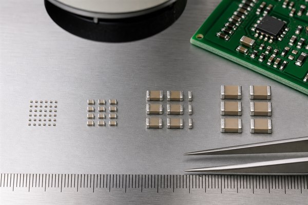
The body-area ratios are mathematical comparisons of nominal length multiplied by nominal width: 0.390625×, 1×, 2.25× and 6.25×. They do not represent the required PCB land pattern or predict routing savings directly. The relative process-demand column assumes comparable component types, equipment and assembly conditions; actual capability must be verified for the selected part and production line.
Use the comparison as a screening tool, not an automatic instruction to choose the smallest option. If 0201 or imperial 0402 meets the enclosure and routing target, it usually offers more visible solder features and a less restrictive handling window. Move to the 01005 component size when the recovered placement area, shorter connection or package availability creates a project-level benefit that can justify tighter printing, inspection and rework controls.
Why Are 01005 Components Used in High-Density Electronics?
The 01005 component size reduces passive-component area where product size, interconnect length or component count limits the layout. Its value is greatest when the released area produces a measurable board-level benefit rather than a smaller footprint in isolation.
- More functions in a fixed outline: smaller bypass, bias and filtering components can free surface area for ICs, shielding, connectors or test access.
- Shorter local connections: placing decoupling components close to an IC power pin can reduce loop length and parasitic inductance, provided the via and plane connection remain well designed.
- Reduced module size: wearables, mobile products, hearing devices, cameras and compact wireless modules often have strict enclosure limits.
- Dense routing options: the smaller courtyard may create additional escape channels, although the finished pad and solder-mask rules determine the actual gain.
- Lower individual component mass: low mass can help placement stability, but paste imbalance and wetting asymmetry still make tombstoning possible.
The trade-off is process cost. Finer paste, tighter stencil and placement control, more capable inspection, feeder management and lower rework yield can outweigh the board-area saving. A practical selection compares the value of the recovered area with the added assembly risk and verification effort.
Quantify the 01005 component size decision on the real layout. Compare the candidate packages by total occupied courtyard, number of released routing channels, distance from the passive to the connected pin, required layer count and accessible test area. Also estimate whether the assembler must introduce a new stencil strategy, feeder type or inspection recipe. A smaller body that does not reduce the board outline or layer count may deliver little commercial benefit.
What Should Be Checked Before Selecting a 01005 Component?
Select the exact part number before finalizing a footprint around the 01005 component size. A size code does not confirm electrical rating, tolerance, temperature behavior, availability, height or termination construction. Use the following sequence to prevent a mechanically correct package from becoming an electrical or supply-chain problem.
- Confirm the electrical requirement. Check resistance or capacitance value, tolerance, voltage, power, temperature coefficient, frequency behavior and aging where applicable.
- Review derating. A tiny resistor or capacitor may fit the schematic but lack the voltage, power or capacitance stability required at operating temperature and bias.
- Lock the package drawing. Record maximum length, width and height plus termination geometry, not only the nominal 01005 body size.
- Check approved land guidance. Compare the supplier recommendation with the PCB fabricator’s finished-copper tolerance and the assembler’s proven footprint.
- Verify machine compatibility. Confirm feeder type, nozzle, vision recognition, component-height range, placement accuracy and minimum supported part size.
- Review finish and storage. Confirm termination finish, moisture or packaging requirements, shelf-life controls and traceable lot information.
- Assess sourcing resilience. Check lifecycle status, lead time, minimum order quantity, reel quantity and continuity of supply.
- Plan inspection and rework. Define how paste, placement and hidden fillets will be verified before committing to production volume.
The 01005 component size selection record should identify the approved MPN, drawing revision, electrical derating basis, package dimensions, termination finish, reel format, approved source and lifecycle status. Add a documented response for shortages or end-of-life notices so purchasing knows when to pause release and escalate the supply risk. This converts the checklist into a controlled release rather than an informal design note.
How Should a 01005 Component Footprint and Pad Size Be Designed?
A reliable footprint for the 01005 component size begins with the supplier’s land recommendation and is then adjusted to the proven PCB and assembly process. There is no universal 01005 component pad size that applies to every resistor, capacitor, finish and soldering process.
- Import the maximum component geometry. Use body and termination tolerances from the exact drawing to define toe, heel and side relationships.
- Choose the land-pattern objective. Decide whether the priority is minimum area, maximum process margin, high component density or easier inspection.
- Set finished copper dimensions. Specify the land at the finished condition and account for etch bias, copper thickness and registration capability.
- Calculate pad-to-pad spacing. Check the inner gap against termination positions, solder bridging risk and the assembler’s paste-release window.
- Define solder-mask geometry. Verify the opening clears both pads at worst-case registration while leaving a manufacturable mask web to adjacent features.
- Control trace entry. Route symmetrically where possible and avoid unequal copper heat sinks that can drive uneven wetting or tombstoning.
- Protect the courtyard. Include placement tolerance, neighboring-component clearance, nozzle access and optical inspection line of sight.
- Run fabrication and assembly DFM. Review Gerber or ODB++ copper, mask and paste layers together rather than approving each layer independently.
- Validate on representative hardware. Use first-article paste and joint data to confirm the selected footprint before volume release.
For dense arrays, check local copper balance and board support as carefully as nominal pad dimensions. Solder-mask registration, panel stretch and board warpage can shift the effective process window across the panel. Record the approved land pattern and prevent uncontrolled library substitutions on repeat builds.
A complete footprint release package should show finished copper length and width, inner gap, mask opening, paste aperture, trace-entry direction, courtyard and reference origin. Include the fabrication tolerance assumptions used in the DFM review. During first-article inspection, measure representative lands and mask clearances at the panel center and edges, then compare the results with the approved geometry before accepting the library for repeat builds.
How Should Stencil Apertures and Solder Paste Be Set for 01005 Components?
Stencil design for the 01005 component size must deposit repeatable, balanced paste volumes on both pads. The correct aperture depends on pad area, stencil thickness, aperture aspect ratio, paste particle distribution, stencil coating, release behavior and neighboring packages. A single stencil thickness chosen for the largest component can overload or starve the 01005 deposits.
- Start from the approved paste layer. Match each aperture to the finished land and required solder volume, not to the nominal component body.
- Check area ratio and release. Confirm that aperture opening area relative to wall area supports consistent transfer for the selected stencil thickness.
- Use suitable paste. Select a particle distribution and flux system proven for the aperture size, storage conditions, print interval and reflow atmosphere.
- Balance left and right deposits. Keep aperture area, stencil-wall condition and local board support consistent to reduce wetting imbalance.
- Separate mixed-package needs. Use local step-down, aperture reduction or another validated method when larger parts require substantially more paste.
- Control the print process. Set squeegee speed, pressure, separation, understencil cleaning and paste replenishment from measured transfer results.
- Verify with SPI. Measure volume, height, area, offset and left-to-right balance; use process capability trends instead of pass/fail inspection alone.
Do not publish a universal 01005 stencil thickness or paste type without knowing the assembler’s equipment and validation data. The useful specification is the controlled deposit window and its measured stability. Trial boards should include representative copper density, board support and neighboring components because isolated coupons can print differently from the product panel.
Define the print acceptance plan before the trial. Record aperture dimensions, stencil thickness, paste lot, time out of refrigeration, print count, cleaning interval and SPI results by panel location. Review average deposit volume together with variation and left-to-right balance; a good average can conceal unstable individual deposits. If mixed packages share the stencil, confirm that changes made for the 01005 component size do not starve connectors, thermal pads or other high-volume joints.
How Are 01005 Components Placed and Reflowed?
For the 01005 component size, verify reel presentation, approve the paste print, use a suitable feeder and nozzle, calibrate vision, and control placement force before running a measured board-level reflow profile. These operations must remain connected so component recognition, paste condition, placement accuracy and thermal balance stay within one verified process window.
- Verify incoming reels. Confirm part number, package code, orientation, tape dimensions, lot traceability and storage status before loading.
- Prepare stable board support. Support the panel beneath dense or thin regions so printing and placement do not flex the board.
- Approve the first print. Use SPI to confirm deposit volume, offset and left-to-right balance at several panel locations.
- Load a suitable feeder and nozzle. Check pocket presentation, pickup height, nozzle condition, vacuum level and component release.
- Program vision from the real part. Teach the correct body and termination contrast; reject rotated, doubled, damaged or poorly centered pickups.
- Control placement force and height. Excess force can squeeze paste or damage the component, while insufficient travel can leave the part unstable on the deposits.
- Minimize process delay. Control the time between printing, placement and reflow to limit paste drying, slumping and contamination.
- Profile the populated assembly. Measure the board, not only oven settings, and meet the paste supplier’s thermal window without overheating sensitive components.
- Correlate post-reflow results. Link AOI findings with SPI, placement and profile data so defects lead to a specific process correction.
Ramp rate, soak behavior, time above liquidus and peak temperature must be validated for the solder paste and the complete assembly. Thermal symmetry around each land matters: unequal pad connection, copper area or shielding can make one termination wet earlier and pull the component upright.
Release production from a representative first article, not from machine setup screens alone. Sample multiple panel locations and review SPI, pickup rejects, placement offsets, AOI defects and electrical-test results together. Preserve the approved machine program, feeder assignment, nozzle reference and measured thermal profile under revision control. Repeat the validation after a stencil, paste, component source, panelization or major machine-program change.
Which Defects Occur During 01005 Assembly and How Can They Be Prevented?
The principal defects for the 01005 component size are tombstoning, open joints, solder bridges, component skew, solder balling and missing components. Prevent them by linking each defect to measured paste volume, placement records, thermal behavior and inspection evidence before changing the process.
| Defect | Likely Cause | Evidence | Prevention |
| Tombstoning | Unequal paste, wetting timing or thermal mass | SPI imbalance, orientation trend, profile data | Balance deposits, pad connections and heating |
| Open joint | Insufficient transfer, offset or poor wetting | Low SPI volume, AOI indication, electrical open | Improve release, alignment, finish and paste condition |
| Bridge | Excess paste, slumping or inadequate spacing | Paste spread, adjacent-joint connection | Reduce deposit, stabilize print and review land gap |
| Skewed component | Placement offset, disturbed paste or asymmetric wetting | Pre-reflow placement data and post-reflow position | Calibrate vision, support board and balance geometry |
| Solder balling | Paste outside land, rapid heating or contamination | Ball location, print image and thermal record | Control aperture, cleanliness and profile |
| Component loss | Poor pickup, nozzle contamination or transfer shock | Placement-machine pickup and reject logs | Maintain feeder/nozzle and verify vacuum settings |
Use defect location and frequency to separate systematic from random causes. A repeated defect in one orientation can indicate thermal or routing asymmetry; a panel-edge trend can point to support or print separation; intermittent defects across feeders can indicate reel presentation or nozzle contamination. Preserve traceability between PCB panel, paste lot, reel lot, machine program and inspection record.
Close the loop with a defect Pareto by type, location, orientation, feeder and time period. Change one controlled variable at a time and confirm the result on another representative run. For example, an open-joint cluster with low SPI volume calls for a printing investigation, while normal deposits combined with placement offsets point toward vision, feeder or board-support control. Record the verified cause and corrective action in the repeat-order process plan.
How Should 01005 Solder Joints Be Inspected and Reworked?
For the 01005 component size, inspect solder joints with SPI before placement, placement-machine records, post-reflow AOI and appropriate electrical testing; use X-ray or destructive analysis only when the investigation requires it. Perform rework under magnification with a qualified thermal method, then verify pad integrity, alignment and electrical function.
- Inspect paste before placement. SPI measures deposit volume, area, height and offset while the process can still be corrected without scrapping populated boards.
- Review placement data. Use pickup, recognition and placement logs to identify feeder, nozzle or vision trends.
- Run post-reflow AOI. Use suitable lighting and magnification to assess presence, alignment, polarity where relevant, solder bridging and visible fillet condition.
- Apply X-ray selectively. X-ray can support investigation of hidden solder distribution, but resolution, contrast and interpretation must be proven for the tiny joint.
- Perform electrical tests. Continuity, in-circuit or functional tests detect opens and shorts that optical inspection may miss, although they may not expose a mechanically weak joint.
- Escalate analysis for recurring defects. Microsectioning or controlled destructive analysis can identify wetting, intermetallic, pad and crack conditions when production evidence is inconclusive.
- Qualify the rework method. Define magnification, tool size, flux, heating, component handling, pad cleaning and maximum exposure before touching a production board.
- Verify after rework. Inspect pad integrity and alignment, repeat relevant electrical tests and record the replaced part and rework history.
Manual soldering with a conventional iron gives poor control at this scale. Local hot-air or other precision methods may still move neighboring components or overheat the laminate. If the board cannot be reworked repeatably without collateral damage, the acceptance plan should favor early process detection and controlled board replacement.
Set 01005 component size acceptance criteria before inspectors review production images. Define what constitutes missing, skewed, bridged or insufficient joints, how electrical failures are escalated and when destructive analysis is justified. The rework instruction should also limit repeat heating and identify adjacent components that require protection or reinspection. Track reworked boards separately so recurring repairs do not hide an unstable printing or placement process.
FAQs About 01005 Components
Q1: Do 01005 resistors and capacitors carry readable value markings?
A1: Usually not. The body is too small for a practical printed value code. Identification therefore depends on the labeled reel, manufacturer part number, feeder position and production traceability. Once parts are removed from controlled packaging, visual appearance alone is not a reliable way to recover their value or rating.
Q2: Can a 01005 component be rotated 90 degrees in the layout?
A2: Rotation is electrically acceptable for many nonpolar passives, but it can change assembly behavior. Check routing symmetry, local copper mass, paste-print direction, placement-machine recognition and AOI programming. On a dense panel, one orientation may show a different tombstoning rate, so validate the actual board instead of assuming orientation has no effect.
Q3: Do 01005 components require special packaging?
A3: They require carrier tape and reels that the selected feeder can present consistently. Pocket geometry, cover-tape peel, component movement and static control affect pickup reliability. Confirm the packaging specification at the part-number level and preserve reel labels for lot traceability; loose handling is unsuitable for routine production.
Q4: Why can 01005 components cling to tweezers, nozzles or nearby surfaces?
A4: Their extremely low mass makes static charge, flux residue and surface contamination more influential. Use grounded ESD controls, clean tools, controlled handling and equipment settings suited to the package. If parts repeatedly remain on a nozzle, inspect the nozzle surface, vacuum release, feeder presentation and environmental conditions.
Q5: Are 01005 components suitable for prototypes?
A5: Yes, when the prototype is built on production-representative equipment. A hand-assembled prototype may prove circuit function but cannot validate paste transfer, placement yield or reflow stability. If volume production will use 01005 parts, include representative panels, stencils, feeders, inspection and test records in the prototype plan.
Q6: How should unused 01005 reels be stored?
A6: Follow the component supplier’s packaging, humidity, temperature, ESD and shelf-life instructions. Keep the original label and lot identity, protect the tape from bending and contamination, and record exposure when required. Storage rules can differ among resistor, capacitor and specialty-part families even when the outline is identical.
Q7: Can 01005 parts be placed on both sides of a PCB?
A7: Yes, but the second reflow and board-handling plan must be qualified. Check whether first-side components remain secure, whether support tooling contacts populated areas, and whether board warpage changes print or placement accuracy. The complete two-sided sequence should be included in the assembly trial.
Q8: Does conformal coating work over 01005 components?
A8: It can, provided coating coverage and cleanliness are controlled. Dense spacing can trap flux residue, bubbles or excess coating around tiny components. Confirm compatibility with the component, solder mask and finish, then inspect representative coated assemblies for coverage, bridging of keep-out areas and repairability.
Q9: Should spare 01005 components be included in the BOM quantity?
A9: Yes, the purchasing quantity should include process attrition. Feeder setup, leader requirements, machine verification and rejected pickups consume parts before good assemblies are completed. Agree the attrition rule with the assembler using reel format, build quantity and placement history rather than applying an arbitrary percentage.
Q10: What data should be sent for an accurate 01005 assembly review?
A10: Send Gerber or ODB++, BOM with manufacturer part numbers, centroid data, assembly drawings and panel information. Add quantity, solder-paste requirements, test scope, inspection criteria and any reliability conditions. Complete data allows footprint, stencil, feeder, placement, reflow and inspection risks to be reviewed together.
The 01005 component size can provide meaningful density when the PCB footprint, printing, placement, reflow and inspection controls are qualified as one assembly process. For an engineering review and quotation, contact EBest Circuit at sales@bestpcbs.com. Send your Gerber or ODB++ files, BOM, centroid data, assembly drawing, order quantity, delivery target and test requirements so the team can evaluate the footprint, stencil, placement and inspection plan.