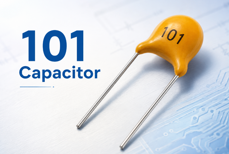
A 101 capacitor has a capacitance value of 100 pF, which equals 0.1 nF or 0.0001 µF. It is commonly used in RF circuits, timing circuits, oscillator circuits, signal filtering, sensor circuits and some high-voltage PCB applications.
The marking “101” follows the standard three-digit capacitor code. The first two digits form the base number, and the third digit shows how many zeros to add in picofarads. Therefore, 101 means 10 with one zero, which equals 100 pF.
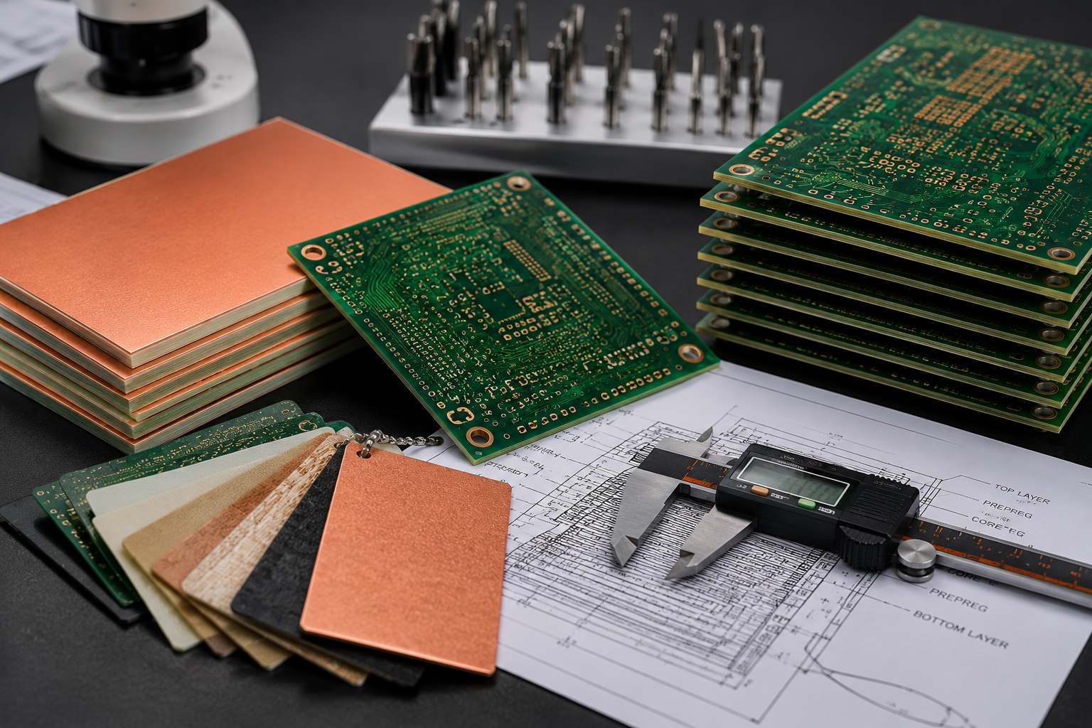
However, the code only tells capacitance. Before using or replacing a 101 capacitor, you should also check voltage rating, tolerance, dielectric material, package size, operating temperature and circuit function. These details decide whether the part can work reliably in the actual PCB assembly.
What is the Value of a 101 Capacitor?
The value of a 101 capacitor is 100 pF. In other units, it equals 0.1 nF and 0.0001 µF. This value is read from the standard three-digit capacitor marking system used on many ceramic capacitors.
To read it, take the first two digits, “10,” as the base number. Then use the third digit, “1,” as the multiplier. This means one zero is added after 10, giving 100 pF.
The most common mistake is reading 101 as 101 pF, 101 nF or 101 µF. That is incorrect. In normal capacitor code reading, the correct result is 100 pF, unless the part uses a special manufacturer-specific marking system confirmed by its datasheet.
What Does 101 Mean on a Capacitor?
The marking “101” on a capacitor means 100 pF capacitance. It is a coded value, not a direct decimal number. This marking is common on ceramic disc capacitors, MLCC capacitors and some high-voltage ceramic capacitors.
| Code | Base | Multiplier | Value |
|---|---|---|---|
| 101 | 10 | 1 zero | 100 pF |
This code does not show whether the capacitor is 50 V, 100 V, 1 kV or 3 kV. It also does not confirm tolerance, dielectric material or package size. Two capacitors may both be marked 101, but they may be designed for very different circuit conditions.
For correct selection, the marking should be checked together with the part number, datasheet, BOM and circuit position.
What Is the 101 Capacitor Value in pF, nF and µF?
The 101 capacitor value is 100 pF, 0.1 nF and 0.0001 µF. These values describe the same capacitance in different units.
| Unit | Value |
|---|---|
| pF | 100 pF |
| nF | 0.1 nF |
| µF | 0.0001 µF |
| F | 0.0000000001 F |
In practical PCB circuits, 100 pF is a small capacitance value. It is usually used for high-frequency signals, RF paths, timing adjustment, signal coupling and noise control.
It should not be confused with 104, which is 0.1 µF. This is a common replacement error because both parts may look like small ceramic capacitors, but their capacitance differs by 1,000 times.
How to Read a 101 Capacitor Code Correctly?
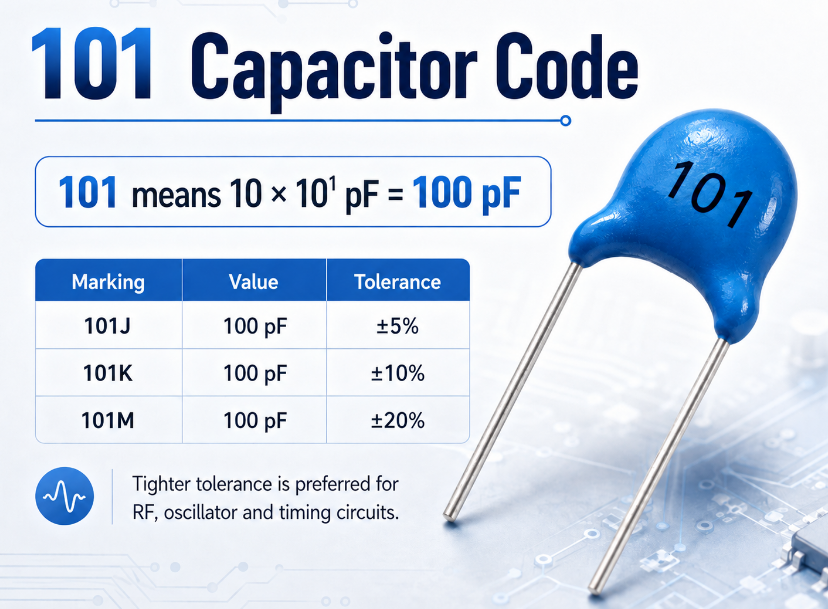
A 101 capacitor code is read in picofarads. The first two digits show the starting number, and the third digit shows how many zeros are added. So 101 means 10 × 10¹ pF = 100 pF.
If a letter appears after the number, such as 101J, 101K or 101M, the letter usually shows tolerance. Tolerance tells how far the actual capacitance may vary from the rated value.
| Marking | Value | Tolerance |
|---|---|---|
| 101J | 100 pF | ±5% |
| 101K | 100 pF | ±10% |
| 101M | 100 pF | ±20% |
For RF, oscillator and timing circuits, tolerance can affect performance. A 101J capacitor may be better than 101K when tighter capacitance control is required. For general high-frequency noise filtering, wider tolerance may be acceptable if the circuit design allows it.
What Is the Capacitance of a 101 Ceramic Capacitor?
A 101 ceramic capacitor has a capacitance of 100 pF. Ceramic is commonly used for this value because it supports compact size, low cost, fast response and good high-frequency behavior.
The actual performance depends on the dielectric material. C0G/NP0 ceramic capacitors offer better stability across temperature, voltage and time. They are suitable for RF circuits, oscillator circuits, timing networks and precision signal paths.
Other ceramic materials, such as X7R, Y5P or Z5U, may be used in less critical filtering circuits. However, their capacitance can change more under voltage and temperature. For RF tuning, sensor signals or timing-related applications, dielectric selection should be checked carefully.
101 Capacitor Datasheet Overview
A 101 capacitor datasheet confirms whether the part can work safely in the target circuit. The marking “101” only means 100 pF. It does not confirm voltage rating, tolerance, dielectric, package size, temperature range, insulation performance or reliability grade.
| Item | Common Detail |
|---|---|
| Capacitance | 100 pF |
| Unit Conversion | 0.1 nF / 0.0001 µF |
| Capacitance Code | 101 |
| Tolerance | ±5%, ±10%, ±20% |
| Voltage Rating | 50 V, 100 V, 500 V, 1 kV, 2 kV, 3 kV |
| Dielectric | C0G, NP0, X7R, Y5P, Z5U |
| Temperature Range | -55°C to 125°C, series-dependent |
| Capacitor Type | MLCC, ceramic disc, high-voltage ceramic |
| Mounting Type | SMD, through-hole |
| Package Size | 0402, 0603, 0805, 1206, disc type |
| Insulation Resistance | Series-dependent |
| Dissipation Factor | Series-dependent |
| Temperature Coefficient | Dielectric-dependent |
| Rated Frequency | Series-dependent |
| Operating Environment | Consumer, industrial, high-voltage, RF |
| Compliance | RoHS, REACH, UL, safety rating when applicable |
| Typical Use | RF, timing, filtering, coupling, snubber |
What Is the Voltage Rating of a 101 Capacitor?
The voltage rating of a 101 capacitor is not defined by the “101” code. The code only means 100 pF. The actual voltage may be 50 V, 100 V, 500 V, 1 kV, 2 kV or 3 kV, depending on the capacitor series.
For low-voltage signal circuits, a 50 V or 100 V part is often enough. For high-voltage supplies, pulse circuits, snubber paths, flyback circuits or surge-related designs, a 101 1kV capacitor or 101 3kV capacitor may be required.
The safe replacement rule is clear: never use a lower voltage rating than the original capacitor. A higher voltage rating may be acceptable, but only if the package size, lead spacing, dielectric type and circuit performance remain suitable.
Voltage margin matters in mass production. If the circuit regularly operates close to the capacitor’s maximum rating, long-term reliability may drop, especially under heat, vibration or voltage spikes.
What Is the Difference Between 101 1kV and 101 3kV Capacitors?
A 101 1kV capacitor and a 101 3kV capacitor both have 100 pF capacitance. The main difference is voltage withstand capability. A 3kV capacitor is designed for higher electrical stress and usually has stronger insulation or a larger body.
| Type | Value | Voltage | Common Use |
|---|---|---|---|
| 101 1kV capacitor | 100 pF | 1,000 V | High-voltage signal, power filtering, snubber circuits |
| 101 3kV capacitor | 100 pF | 3,000 V | Surge circuits, pulse circuits, high-voltage applications |
A 3kV capacitor can often replace a 1kV capacitor if physical size and circuit behavior allow. However, a 1kV capacitor should not replace a 3kV part. The lower voltage rating may cause dielectric breakdown, leakage current increase, overheating or early field failure.
In PCB assembly, this difference should be confirmed during BOM review. If the voltage rating is missing, wrong sourcing becomes more likely.
Where Is a 101 Capacitor Commonly Used?
A 101 capacitor is used in circuits that require small capacitance, fast response and high-frequency behavior. Because its value is only 100 pF, it is not used as the main energy storage capacitor.
Common applications include:
- RF circuits: used for antenna matching, tuning and signal coupling.
- Oscillator circuits: helps adjust frequency and timing behavior.
- Signal filtering: removes high-frequency noise from sensitive lines.
- Sensor circuits: stabilizes small analog signals and reduces interference.
- Snubber circuits: helps control voltage spikes in selected high-voltage designs.
- Communication modules: supports RF paths, clock lines and impedance-sensitive circuits.
- PCB repair: replaces damaged ceramic capacitors when value, voltage and package match.
For best performance, placement matters. A 101 capacitor used for filtering should be close to the related IC pin, connector, signal trace or noise source. Long traces add parasitic inductance and reduce filtering effectiveness.
How to Choose the Right 101 Capacitor Replacement?
To choose the right 101 capacitor replacement, match capacitance, voltage rating, tolerance, dielectric, package size and circuit function. The marking “101” alone is not enough.
Use these practical checks:
- Match capacitance: choose 100 pF, equal to 0.1 nF or 0.0001 µF.
- Match voltage: use the same or higher rating when size and performance allow.
- Match tolerance: keep ±5%, ±10% or ±20% according to the circuit requirement.
- Match dielectric: use C0G/NP0 for RF, oscillator and precision circuits.
- Match package: confirm SMD size, body diameter or lead spacing.
- Check circuit role: filtering, timing, coupling and snubber use may require different specifications.
- Avoid unsafe substitution: do not replace high-voltage or safety-rated parts with common ceramic capacitors.
- Approve equivalents early: prevent sourcing delays during mass production.
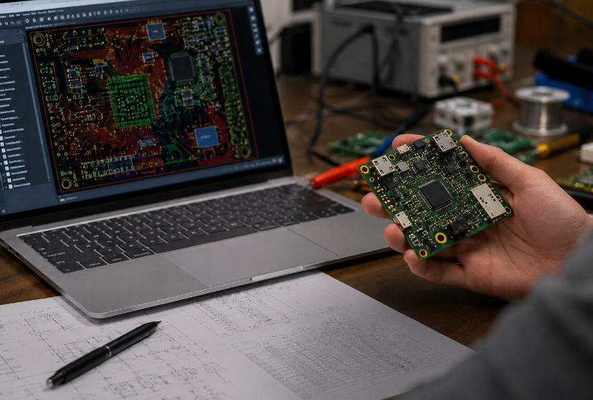
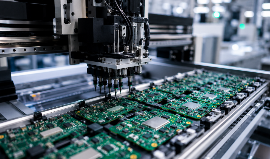
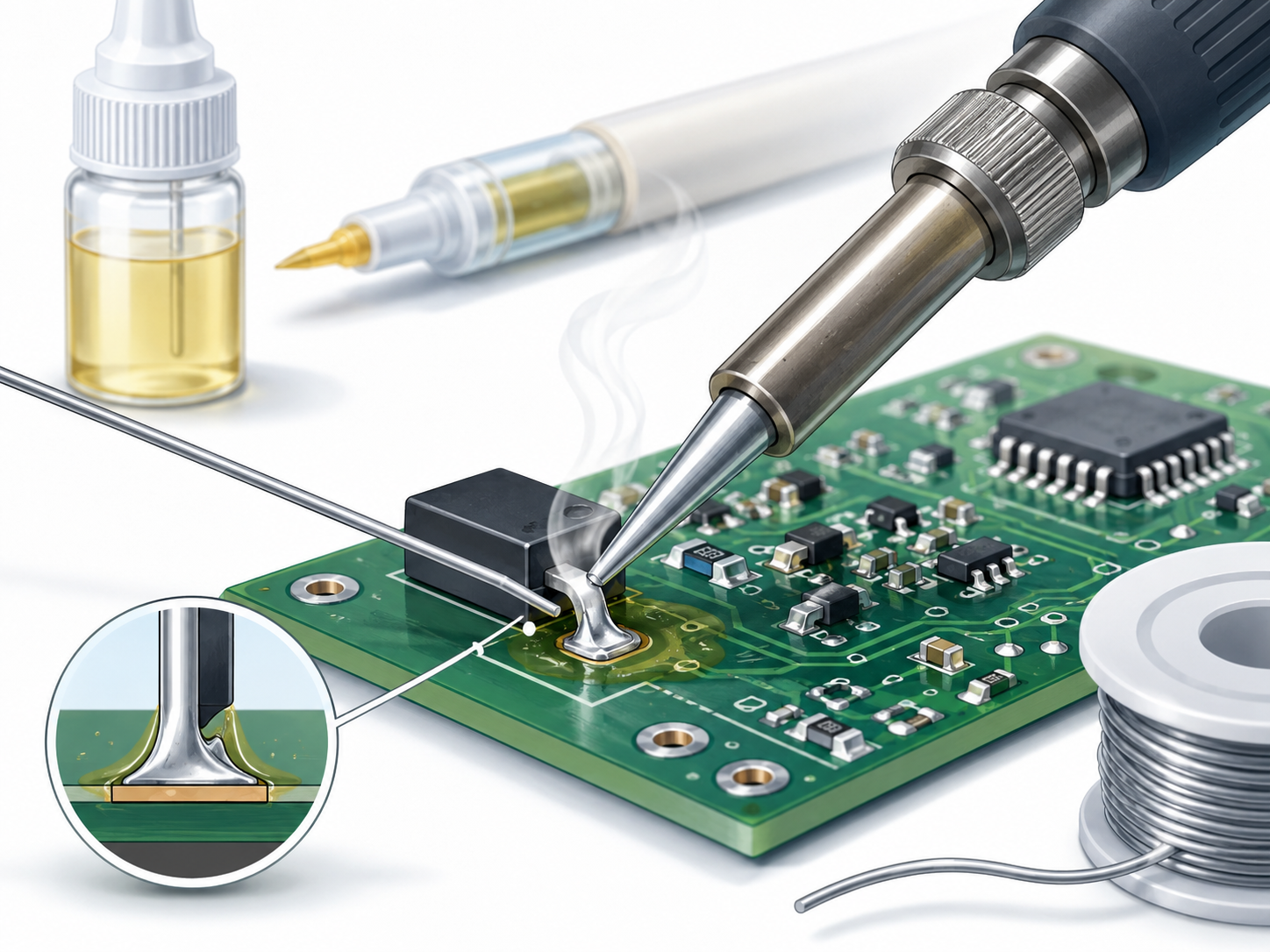
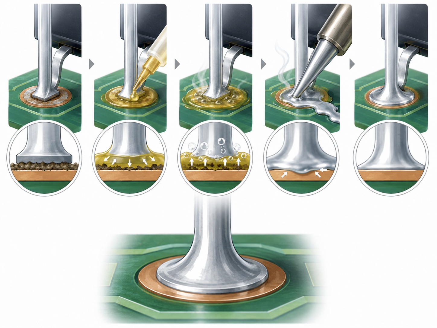
For PCB repair, the safest method is to identify the original part number or compare it with the schematic and BOM. For PCBA production, replacement should be approved before purchasing.
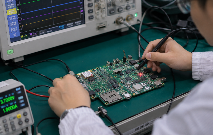
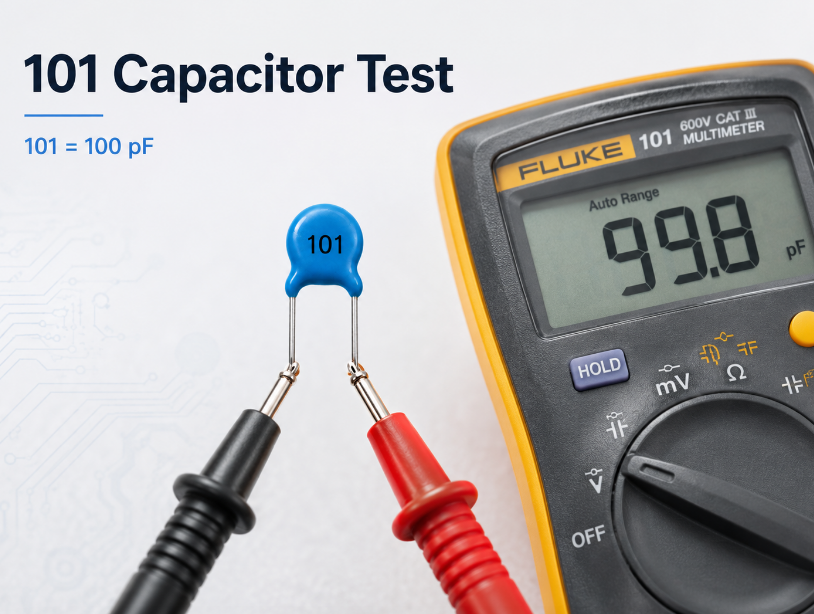
How to Test a 101 Capacitor with a Multimeter?
A 101 capacitor is 100 pF, so the reading is easily affected by test leads and nearby components. A multimeter can be used for quick checking, but an LCR meter is better for accurate testing.
- Power off the PCB
Disconnect power before testing. If the 101 capacitor is used in a high-voltage circuit, discharge the circuit first to avoid meter damage or safety risk. - Confirm the marking
Check whether the part is marked 101, 101J, 101K or 101M. The code confirms 100 pF, while the letter shows tolerance. - Avoid in-circuit testing when accuracy matters
Nearby components and PCB traces can affect the result. Remove the capacitor or lift one lead before measuring if the reading must be accurate. - Set the meter to capacitance mode
Use the capacitance function on the multimeter or Fluke 101. Connect the probes to both terminals and wait for the value to stabilize. - Keep the leads short
Long probes add stray capacitance. Keep the leads short and do not touch the metal probe tips during measurement. - Check the reading against tolerance
A good 101 capacitor should read close to 100 pF. 101J is usually ±5%, 101K is usually ±10%, and 101M is usually ±20%. - Check for short or open failure
Near-zero resistance may indicate a short. No capacitance reading or a value far below 100 pF may indicate an open or damaged capacitor. - Use an LCR meter for precise testing
For RF circuits, oscillator circuits, sensor circuits or PCBA inspection, use an LCR meter instead of a basic multimeter. - Do not rely only on capacitance
In high-voltage circuits, also check leakage, insulation resistance and voltage withstand performance. - Replace with matching specifications
If the capacitor is abnormal, replace it with a 100 pF part that matches the original voltage rating, tolerance, dielectric, package size and safety requirement.
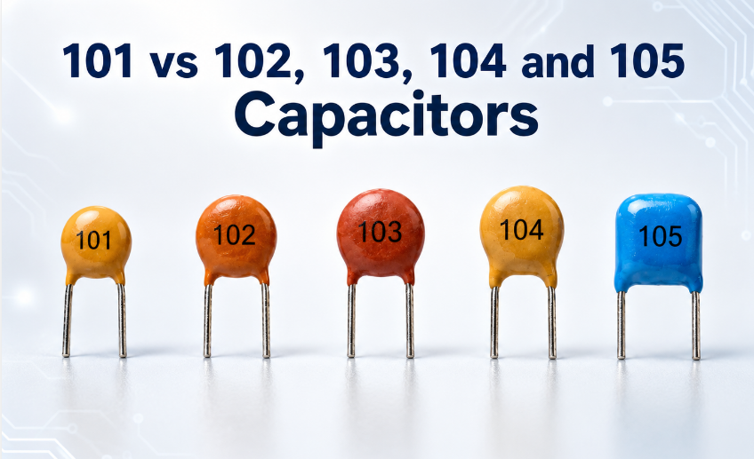
101 vs 102, 103, 104 and 105 Capacitors: What Is the Difference?
The difference between 101, 102, 103, 104 and 105 capacitors is capacitance value. They use the same three-digit code rule, but the multiplier is different.
| Code | pF | nF | µF |
|---|---|---|---|
| 101 | 100 pF | 0.1 nF | 0.0001 µF |
| 102 | 1,000 pF | 1 nF | 0.001 µF |
| 103 | 10,000 pF | 10 nF | 0.01 µF |
| 104 | 100,000 pF | 100 nF | 0.1 µF |
| 105 | 1,000,000 pF | 1,000 nF | 1 µF |
The key warning is simple: 102 is 10 times larger than 101, 103 is 100 times larger, and 104 is 1,000 times larger. These parts should not be treated as direct replacements.
In real circuits, this difference can change filtering cutoff, timing delay, RF matching and signal response. Always confirm the schematic or BOM before replacing one code with another.
FAQs About 101 Capacitor Value, Code and Marking
Q1: Can a 102 capacitor replace a 101 part?
A1: Usually not. A 101 part is 100 pF, while a 102 capacitor is 1,000 pF. That is 10 times higher. In RF, timing, oscillator or filter circuits, this change may shift frequency, slow response or reduce signal quality. Only use 102 if the circuit design clearly allows it.
Q2: Can I replace a 101 marking with a 100 pF capacitor?
A2: Yes, if the other specifications match. The 101 marking is the coded form of 100 pF. The replacement part should also match the original voltage rating, tolerance, dielectric type, package size and safety requirement. For PCBA production, the substitute should be approved before purchasing.
Q3: Can I use a 104 capacitor instead of a 101 coded part?
A3: No in most cases. A 104 capacitor is 0.1 µF, while a 101 coded part is 0.0001 µF. The 104 value is 1,000 times larger. This can completely change filtering, timing or RF behavior and may cause circuit malfunction.
Q4: Why do some 101 capacitors have letters after the number?
A4: Extra letters usually show tolerance, temperature characteristic or manufacturer series information. For example, 101J often means 100 pF ±5%, and 101K often means 100 pF ±10%. The number shows capacitance, while the letters help confirm accuracy or stability.
Q5: Do 101 ceramic parts have polarity?
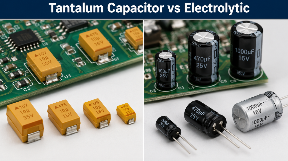
A5: Most 101 ceramic parts are non-polarized, so they can be installed in either direction. This is different from many electrolytic capacitors. However, non-polarized does not mean universal. The part still must match the correct voltage, dielectric, tolerance and package.
Q6: Why is one 100 pF ceramic capacitor larger than another?
A6: Physical size depends on voltage rating, dielectric material, package type and construction. A 3kV 100 pF ceramic capacitor is usually larger than a low-voltage version because it needs stronger insulation and wider spacing. Same capacitance does not always mean same body size.
Q7: Can 101 capacitors be used in high-voltage circuits?
A7: Yes, but only if the voltage rating is suitable. A normal low-voltage 100 pF part should not be used in a high-voltage circuit. For high-voltage use, select a 1kV, 2kV or 3kV version according to the circuit requirement.
Q8: Why does a replacement part fail after assembly?
A8: Common reasons include wrong voltage rating, wrong dielectric, poor soldering, package mismatch or using a non-approved equivalent. If the original component was a high-voltage or C0G/NP0 part, replacing it with a general ceramic capacitor may cause instability or early failure.
Q9: Can this 100 pF component be tested while still on the PCB?
A9: It can be checked quickly in-circuit, but the result may not be accurate. Nearby traces, IC pins and other capacitors can affect the reading. For a reliable test, remove the part or lift one lead. For 100 pF parts, an LCR meter gives better accuracy than a basic multimeter.
Q10: Why does my multimeter not show 100 pF exactly?
A10: A 100 pF capacitor has a very small value, so test leads and stray capacitance can affect the reading. Also, tolerance allows variation. For example, 101K may vary by ±10%. A small difference from 100 pF is normal if it stays within the rated tolerance.
Q11: What happens if the wrong 100 pF part is used in an RF circuit?
A11: RF circuits are sensitive to capacitance value, dielectric loss and layout. A wrong replacement may cause poor antenna matching, weak signal, frequency shift or unstable communication. For RF use, C0G/NP0 dielectric is often preferred because it gives better stability and lower loss.
Q12: What should be checked before buying 101 capacitors in bulk?
A12: Before bulk purchasing, confirm 100 pF value, voltage rating, tolerance, dielectric, package size, approved brand, datasheet and lead time. For PCBA orders, also confirm reel packaging, traceability and substitute part approval. This reduces wrong sourcing and production delays.
Q13: Is this small-value capacitor suitable for power supply decoupling?
A13: It can help suppress very high-frequency noise, but it is not enough for normal power rail decoupling. The value is only 100 pF. Most power supply decoupling designs use larger capacitors such as 0.1 µF, 1 µF or 10 µF, depending on the circuit.
Q14: Why should a PCBA supplier review this capacitor before assembly?
A14: A PCBA supplier should check it because the marking alone is not enough. The same code may appear on different voltage ratings, dielectrics and packages. BOM review helps prevent wrong part sourcing, assembly mismatch, functional failure and rework cost.
Q15: What files help a supplier source the correct 100 pF part?
A15: The best files include the BOM, schematic, PCB layout, part number, datasheet and quantity requirement. If the original part is unavailable, the supplier can use these files to recommend an equivalent component with matching voltage, dielectric, tolerance and package.
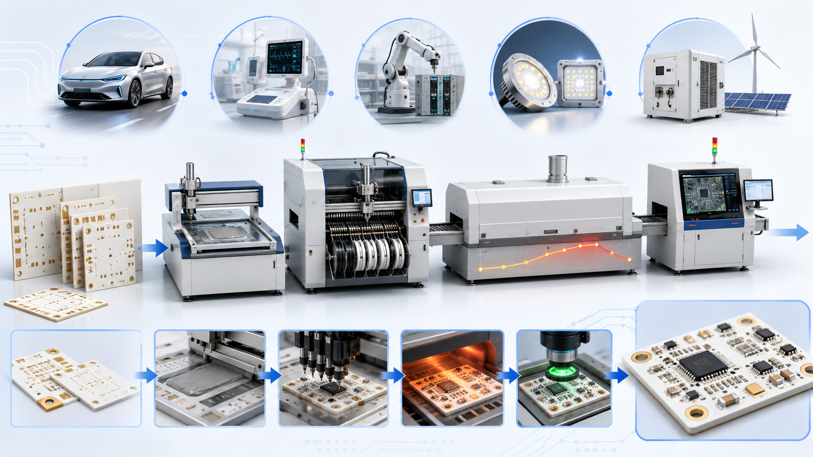
EBest Circuit provides one-stop PCBA service, including BOM review, component sourcing, PCB fabrication, SMT assembly, through-hole assembly and functional testing. For capacitor selection, replacement or custom PCBA production, send your project files to sales@bestpcbs.com for a fast quotation.