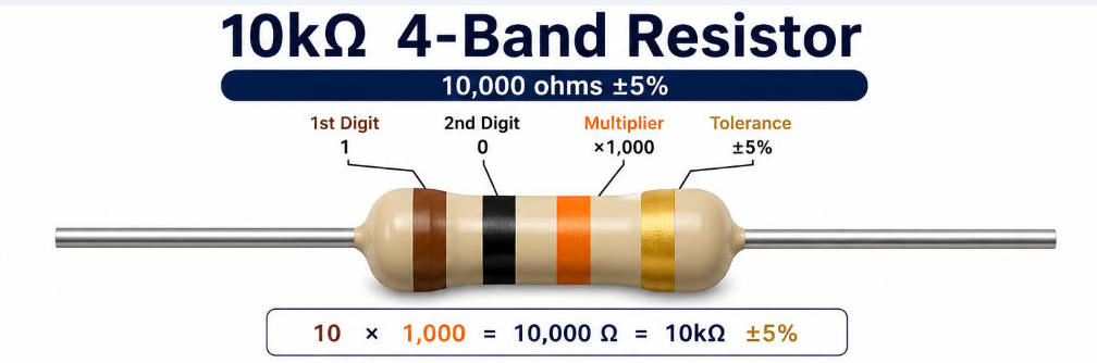
The standard 10k resistor color code is brown-black-orange for a 3-band value reading. A common 4-band 10k resistor is brown-black-orange-gold, meaning 10,000 ohms with ±5% tolerance.
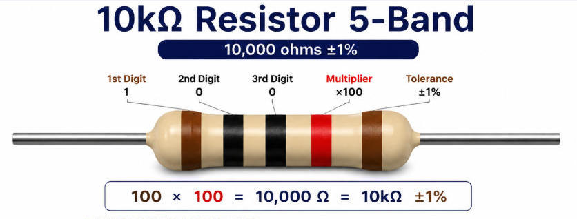
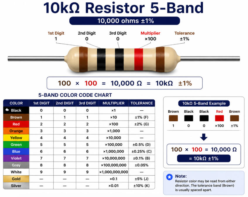
A common 5-band 10k resistor is brown-black-black-red-brown, meaning 10,000 ohms with ±1% tolerance.
A 10k resistor equals 10,000 ohms, or 10 kΩ. It is one of the most widely used resistor values in PCB circuits for pull-up, pull-down, voltage dividers, sensor inputs, timing networks, biasing circuits, and signal conditioning.
What Is a 10k Resistor?
A 10k resistor is a passive electronic component with a resistance value of 10,000 ohms. The letter k means kilo, so 10kΩ = 10 × 1,000Ω = 10,000Ω. In a circuit, a 10k resistor limits current, divides voltage, sets logic levels, or stabilizes input signals.
Why Is the 10k Resistor Color Code Important?
The 10k resistor color code is crucial to identify the resistor value before soldering, testing, repair, or replacement. Wrong resistor values can cause incorrect voltage levels, unstable sensor readings, MCU boot failure, weak pull-up signals, timing errors, or excessive current.
How Does a Resistor Color Code Work?
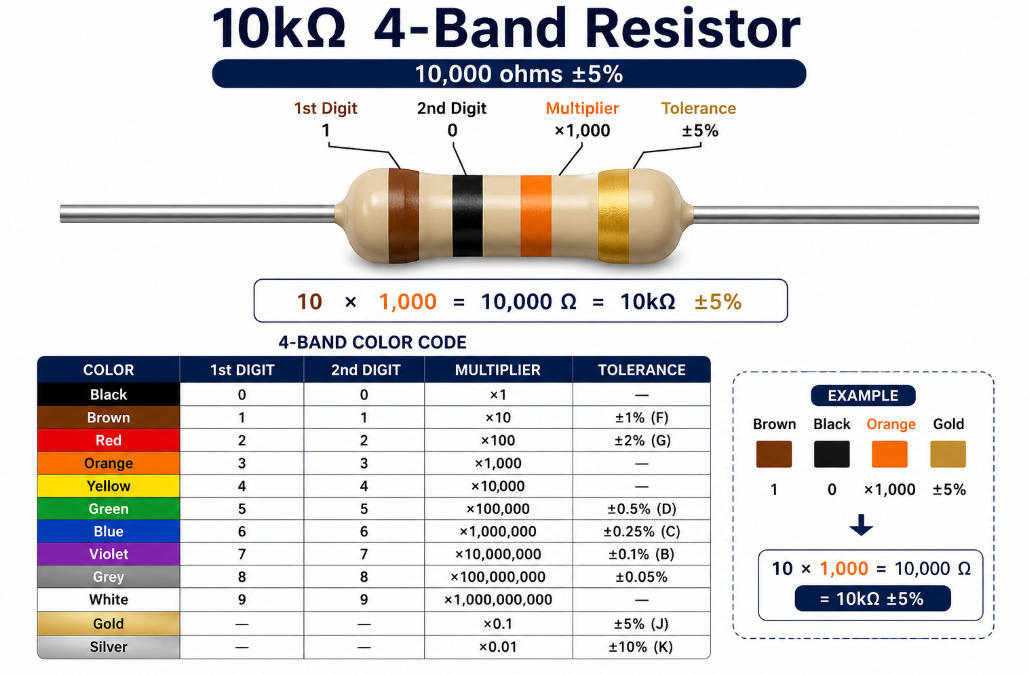
A resistor color code works by using colored bands to represent digits, multipliers, tolerance, and sometimes temperature coefficient.
Color
Digit
Multiplier
Common Tolerance
Black
0
×1
–
Brown
1
×10
±1%
Red
2
×100
±2%
Orange
3
×1,000
–
Yellow
4
×10,000
–
Green
5
×100,000
±0.5%
Blue
6
×1,000,000
±0.25%
Violet
7
×10,000,000
±0.1%
Gray
8
×100,000,000
±0.05%
White
9
×1,000,000,000
–
Gold
–
×0.1
±5%
Silver
–
×0.01
±10%
What Is the 4-Band 10k Resistor Color Code?
The 4-band 10k resistor color code is brown, black, orange, gold for a ±5% resistor. Calculation: 10 × 1,000 = 10,000Ω = 10kΩ.
What Is the 5-Band 10k Resistor Color Code?
The 5-band 10k resistor color code is brown, black, black, red, brown for ±1% precision. Calculation: 100 × 100 = 10,000Ω = 10kΩ.
10k Resistor Color Bands Compared: 4-Band vs 5-Band
Type
Color Bands
Value
Tolerance
Best Use
4-band
Brown-black-orange-gold
10kΩ
±5%
General pull-up, pull-down, LED signal circuits
5-band
Brown-black-black-red-brown
10kΩ
±1%
Precision sensor, reference voltage, industrial control
6-band
Value bands + tolerance + TCR band
10kΩ
Depends
Temperature-sensitive circuits
How to Read a 10k Resistor Color Code Correctly?
Place the tolerance band on the right, read left to right. For brown-black-orange-gold, brown=1, black=0, orange=×1,000, gold=±5%, resulting in 10kΩ ±5%.
What Is the 10k Surface Mount Resistor Code?
Common SMD markings: 103 (10+3 zeros = 10kΩ) or 1002 (100+2 zeros = 10kΩ).
Materials, Features, and Advantages
10k resistors may be carbon film, metal film, thick film SMD, thin film SMD, or wirewound. Features: 10kΩ value, ±5% or ±1% tolerance, through-hole or SMD packages, moderate power rating, widely applicable.
Applications in PCB Design
Used for pull-up/pull-down circuits, voltage dividers, sensor interfaces, timing, transistor bias, communication line biasing, and general PCB logic stabilization.
Procurement and Manufacturing Tips
Check BOM, package, tolerance, power rating, and source reliability. Use AOI and electrical testing in mass production. Confirm resistor value to avoid wrong placements or rework.
Testing and Quality Standards
Verify with multimeter, LCR meter, flying probe, or functional testing. Factory quality standards include component inspection, IPC workmanship, solder joint inspection, and traceability.
Common Failures and How to Avoid Them
Failures include wrong value, cracked body, poor solder, overheating, color misreading. Avoid by BOM confirmation, correct reel loading, process verification, and first-article inspection.
FAQs About 10k Resistor Color Code
What is the 10k ohm resistor color code? Brown-black-orange for 3-band; brown-black-orange-gold for 4-band ±5%.
What is the 4 band 10k resistor color code? Brown, black, orange, gold; 10 × 1,000 = 10kΩ ±5%.
What is the 5 band 10k resistor color code? Brown, black, black, red, brown; 100 × 100 = 10kΩ ±1%.
What does brown black orange gold resistor mean? 10kΩ ±5%, standard 4-band through-hole resistor.
What are the 10k resistor colors? Brown, black, orange for value; gold for ±5% tolerance; 5-band: brown-black-black-red-brown.
How do you read a 10k resistor color code? Place tolerance band right, read left-to-right, convert colors to digits, apply multiplier.
What is the 10k surface mount resistor code? 103 or 1002 markings; 10kΩ SMD resistor.
Is a 103 resistor the same as a 10k resistor? Yes, 103 = 10kΩ.
What is a 10k linear potentiometer pinout? Three pins: two ends of resistive track, middle wiper; wiper output changes as shaft rotates.
Can I replace a 10k resistor with another value? Only after circuit verification; different values may alter voltage, bias, timing.
Conclusion
The 10k resistor color code varies with 4-band or 5-band type: 4-band is brown-black-orange-gold, 5-band is brown-black-black-red-brown. SMD markings include 103 or 1002. For precision applications, choose appropriate tolerance and material type.
If you need keywords-related products or services, EBest PCB can support PCB manufacturing, PCB assembly, OEM production, ODM development, sample builds, batch production, and custom engineering solutions.
If you’re sourcing reliable PCB/PCBA manufacturing — OEM, ODM, prototyping, mass production, or custom engineering solutions — reach out to our engineering team for technical support and a quote at sales@bestpcbs.com.
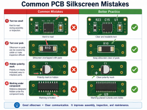
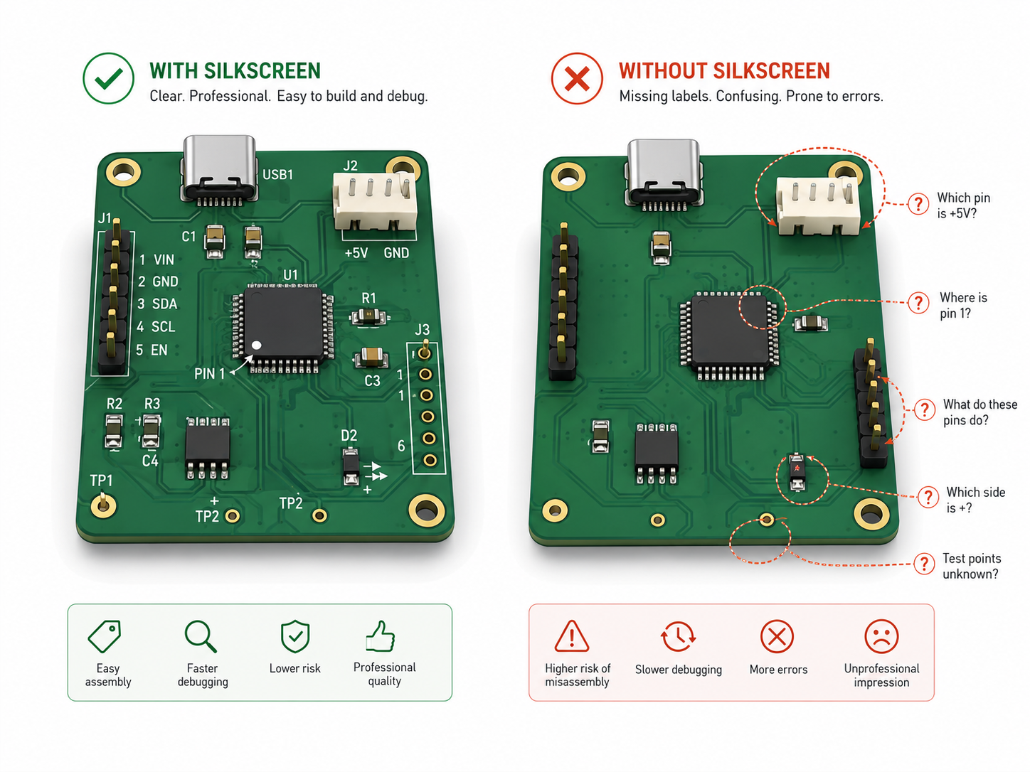
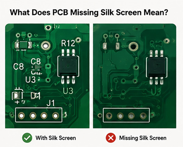
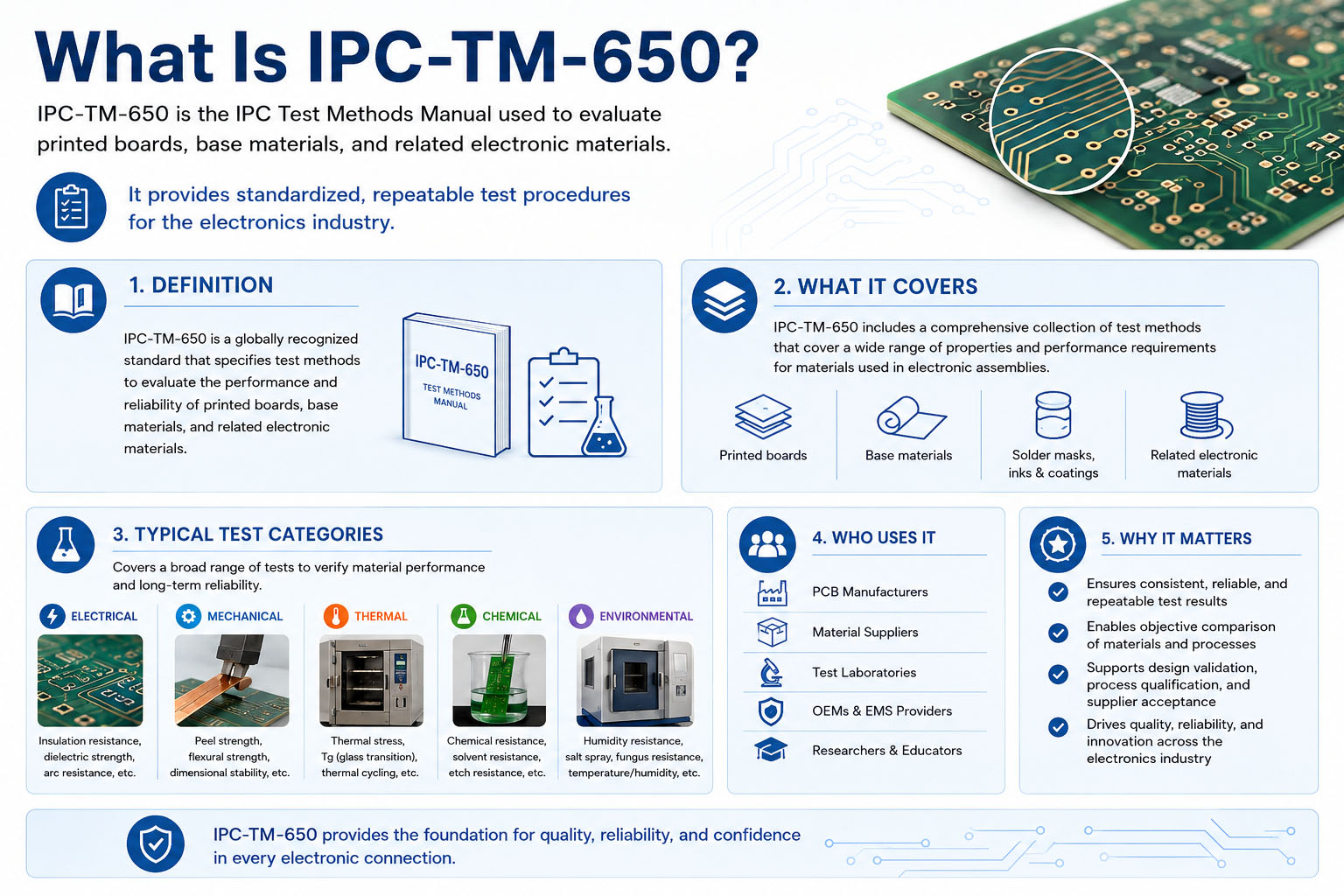
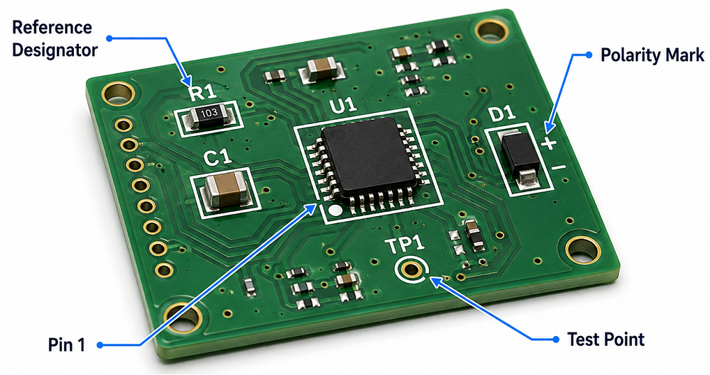
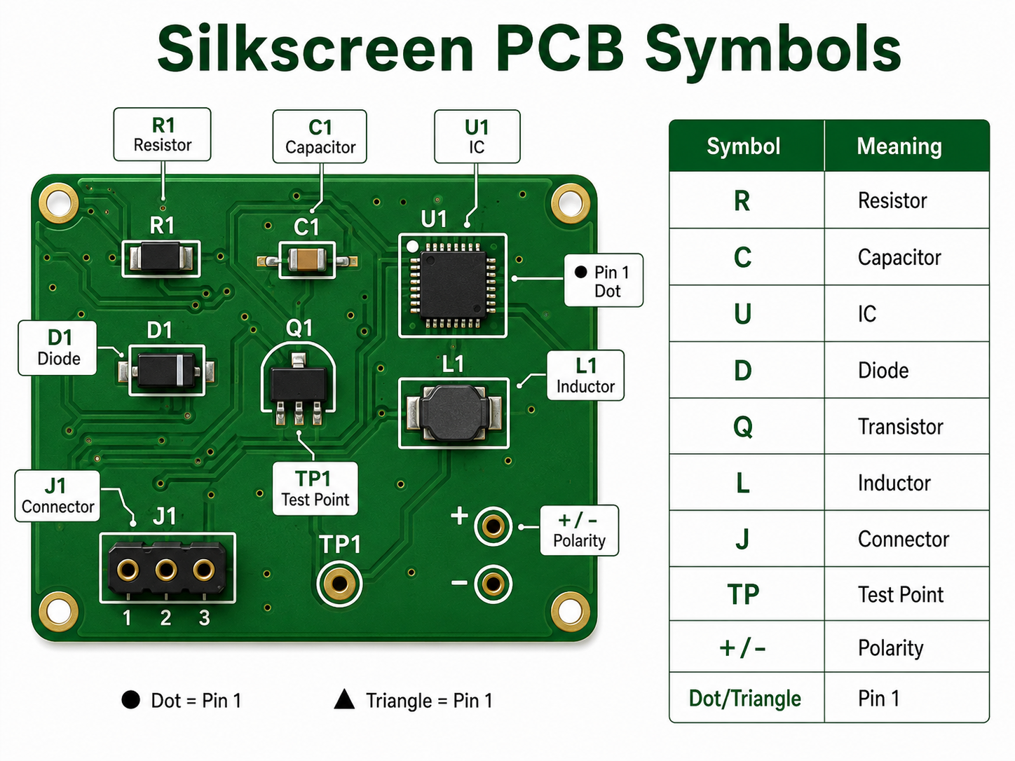
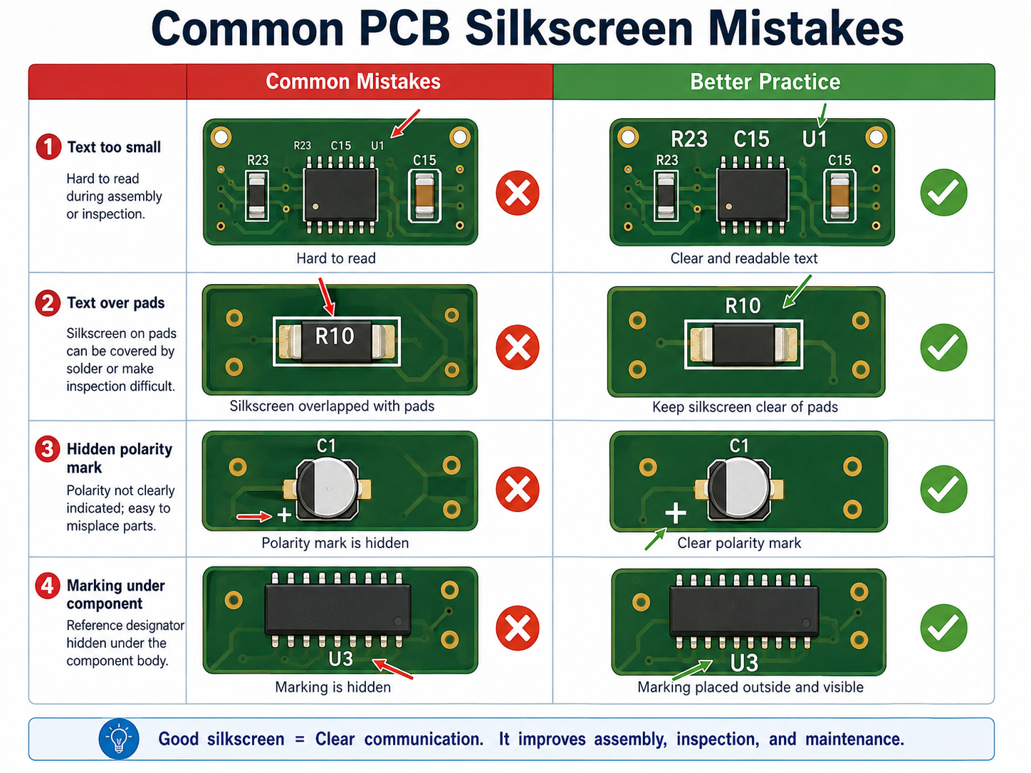
A PCB missing silk screen usually does not stop the bare circuit board from conducting electricity, but it can create real problems during assembly, inspection, testing, repair, traceability, and field maintenance. The silkscreen, also called the legend layer or overlay layer, carries human-readable information such as reference designators, polarity marks, pin-1 indicators, connector labels, warning symbols, part numbers, revision codes, date codes, and compliance marks.
When this information is missing, operators may need to rely only on drawings, pick-and-place data, BOM files, and test fixtures. This increases handling time and raises the risk of assembly mistakes, especially in high-mix, low-volume PCB assembly or custom OEM production.
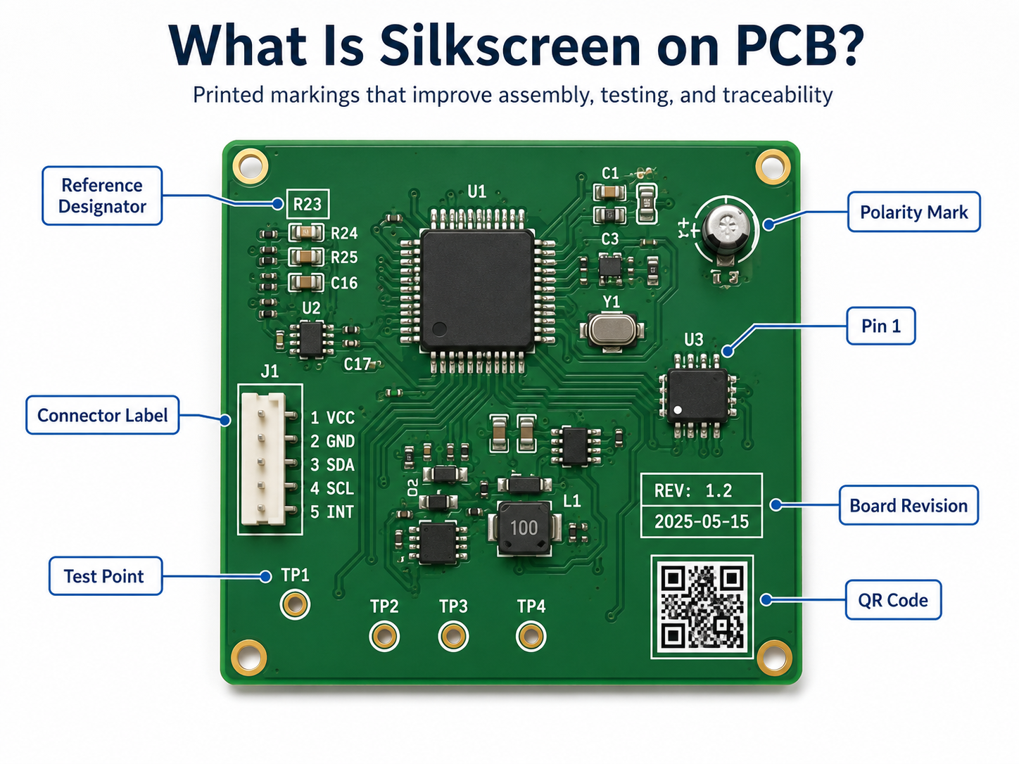
What Is PCB Silkscreen?
PCB silkscreen is the printed marking layer on the top side, bottom side, or both sides of a printed circuit board. It is not a conductive copper layer. Its main role is to show readable information for engineers, assemblers, inspectors, test technicians, and repair teams.
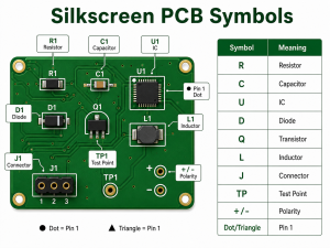
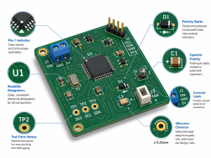
Typical PCB silkscreen content includes component reference designators such as R12, C8, U3, Q1, and J2. It also includes pin-1 marks for ICs, BGAs, connectors, and modules, as well as polarity marks for diodes, LEDs, tantalum capacitors, and electrolytic capacitors.
Silkscreen can also show connector names, test point labels, switch positions, jumper instructions, board names, version numbers, date codes, lot codes, QR codes, logos, warning marks, and compliance symbols.
Why Is Silkscreen Important on a PCB?
Silkscreen is important because it connects digital design data with real production handling. A PCB file may contain perfect information, but once the board reaches SMT, DIP assembly, inspection, testing, or field repair, technicians need fast visual confirmation.
A good silkscreen helps people answer simple but critical questions:
Where is U1?
Which side is pin 1?
Which connector is power input?
Which LED direction is correct?
Which test point should be used for voltage measurement?
Which board revision is this?
Is this product compliant with the required marking plan?
PCB silkscreen is a low-cost layer that improves production clarity. In dense PCB layouts, not every marking can be printed, so the most important information should be prioritized.
What Happens When a PCB Is Missing Silk Screen?
When a PCB is missing silk screen, the electrical circuit may still work if the copper, solder mask, drilling, plating, surface finish, and assembly are all correct. The main risk is not usually immediate electrical failure. The main risk is human error.
A missing silkscreen can cause:
Slower SMT line setup and first article inspection
Higher chance of wrong component orientation
More difficult manual soldering and rework
More time spent checking assembly drawings
Confusion during functional testing
Harder field troubleshooting
Weak traceability when part numbers, revision marks, date codes, or UL-related markings are required
More communication between the customer, PCB manufacturer, and assembly factory
For prototypes, this may only delay engineering review. For batch production, especially OEM and ODM projects, the cost can be much higher because one small orientation mistake may affect hundreds or thousands of boards.
Does Missing Silkscreen Affect PCB Function?
In most cases, missing silkscreen does not directly affect electrical performance. The silkscreen ink does not carry current, define impedance, create insulation between copper layers, or control solder joint formation when it is correctly kept away from pads.
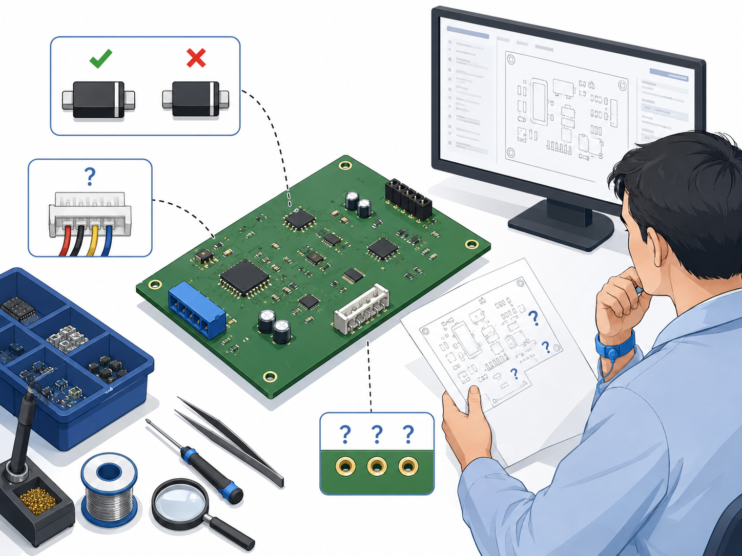
However, it can indirectly affect product function if it leads to assembly mistakes. For example, if a diode polarity mark is missing and the assembly team installs the diode in the wrong direction, the circuit may fail. If a connector pinout is missing, cable installation may become confusing. If test point labels are absent, technicians may probe the wrong point during debugging.
How Does PCB Silkscreen Work in Manufacturing?
PCB silkscreen is generated from the top overlay and bottom overlay layers in PCB design software. During CAM engineering, the PCB manufacturer checks whether the silkscreen overlaps exposed copper pads, solder mask openings, vias, fiducials, or other features where ink should not be printed.
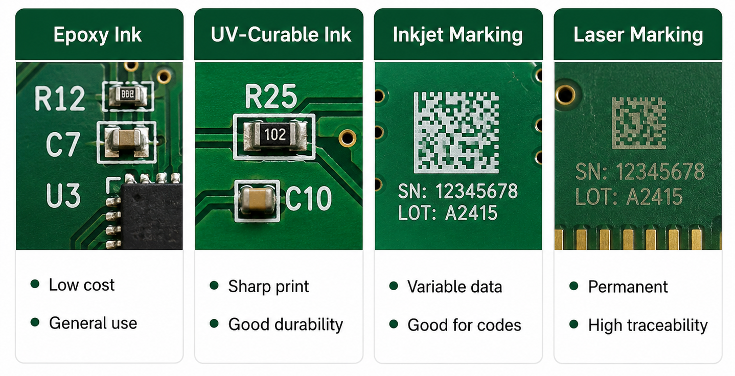
Silkscreen can be applied by several methods:
Method
Common Use
Main Benefit
Main Limitation
Screen printing
Standard PCB production
Cost-effective for volume
Less suitable for very fine text
Liquid photo imaging
Higher precision legend work
Better definition
Higher process requirement
Direct legend printing
Digital printing and flexible data marking
Good for variable data, QR codes, and serial numbers
Equipment and process control matter
Inkjet printing
Modern production, short runs, custom data
Fast changeover
Ink adhesion and readability must be verified
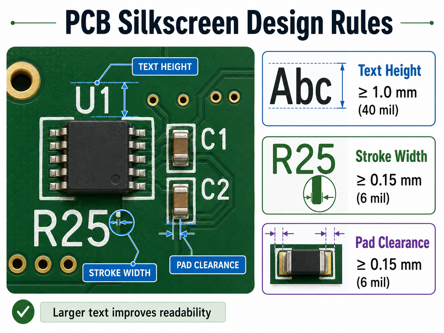
The printing method influences the minimum text height, line width, clearance, registration tolerance, and final readability. This is why a design that looks clear in CAD may become unreadable or partially deleted after CAM cleanup if it violates factory capability.
Main Types of PCB Silkscreen Information
Not all silkscreen information has equal value. In a compact PCB, engineers should rank the markings by production and service importance.
Silkscreen Type
Examples
Priority Level
Why It Matters
Polarity marks
+, -, cathode band, anode mark
Very high
Prevents reversed components
Pin-1 indicators
Dot, triangle, chamfer, notch
Very high
Helps IC and connector orientation
Reference designators
R1, C2, U5, J3
High
Supports inspection and rework
Test point labels
TP1, GND, 3V3, VBAT
High
Speeds up debugging and FCT
Connector labels
VIN, OUT, UART, CAN, USB
High
Reduces cable installation errors
Warning marks
HV, HOT, ESD, polarity warning
High
Improves operational safety
Revision and date codes
Rev A, date code, lot code
Medium to high
Supports traceability
Logos
Brand or customer logo
Low to medium
Useful for identification, not usually functional
Decorative marks
Icons or non-critical graphics
Low
Should not replace technical marks
For production boards, the most valuable silkscreen content is the information that prevents assembly errors, wiring mistakes, test confusion, and traceability gaps.
Common Reasons Why PCB Silkscreen Is Missing
A PCB missing silk screen can come from design files, CAM processing, manufacturing limitations, or production control issues. The root cause must be identified before deciding whether the boards can be accepted, reworked, or remade. The most common reasons that causes PCB silkscreen missing including:
Cause
What Usually Happens
How to Prevent It
Silkscreen Gerber layer not exported
Entire legend layer is absent
Check Gerber output before release
Top and bottom overlay layers confused
Markings appear on the wrong side or disappear
Review layer mapping in CAM
Silkscreen placed over pads
CAM removes the text automatically
Keep sufficient clearance from exposed pads
Text too small
Characters become unreadable or broken
Follow factory minimum text height and line width
Wrong polarity in Gerber data
White or clear areas are inverted
Use Gerber viewer and confirm polarity
Solder mask color conflict
Low contrast makes markings look missing
Choose suitable ink color
Ink adhesion issue
Text fades, peels, or becomes patchy
Control curing, cleaning, and ink quality
Registration shift
Text moves away from target area
Calibrate printing process
Dense layout without cleanup
Labels overlap or become clipped
Clean silkscreen during DFM review
A common engineering mistake is treating silkscreen as the last cosmetic step. In reality, silkscreen should be reviewed during layout, DFM, and first article inspection.
Missing Silkscreen vs. Poor Silkscreen vs. Wrong Silkscreen
These three problems are different and should not be handled the same way.
Issue
Meaning
Typical Risk
Severity
Missing silkscreen
Marking is absent
Slower assembly, unclear orientation, traceability gap
Wrong silkscreen can be more dangerous than no silkscreen. If a diode polarity mark is absent, an operator may stop and verify the drawing. If the polarity mark is printed incorrectly, the operator may trust the board and assemble the component in the wrong direction. This is why silkscreen verification should be part of engineering release, not only final appearance inspection.
PCB Silkscreen Materials and Printing Colors
Most PCB silkscreen is printed with epoxy-based or UV-curable ink. White is the most common color because it provides strong contrast on green, blue, red, black, and purple solder mask. Black silkscreen is common on white solder mask and some aluminum PCB LED boards.
Solder Mask Color
Common Silkscreen Color
Readability
Green
White
Excellent
Blue
White
Very good
Red
White
Very good
Black
White
Good, but glare should be checked
White
Black
Excellent
Yellow
Black
Good
Matte black
White or light gray
Good if ink thickness is stable
For high-end industrial boards, the ink must remain readable after reflow soldering, cleaning, conformal coating, handling, and long-term service. If the PCB will pass through harsh cleaning, coating, potting, or thermal cycling, the manufacturer should confirm ink adhesion and marking durability before mass production.
Design Rules to Prevent Missing Silkscreen
Good silkscreen design starts before Gerber export. Engineers should not wait until CAM asks for confirmation.
A practical design checklist includes:
Keep silkscreen away from pads, exposed copper, fiducials, tooling holes, and solder mask openings.
Use readable text size and line width based on the PCB factory’s capability.
Place reference designators close to the correct component.
Avoid placing important labels under components.
Mark pin 1 clearly for ICs, connectors, modules, and BGAs.
Mark polarity for diodes, LEDs, tantalum capacitors, electrolytic capacitors, and polarized connectors.
Use consistent text orientation, preferably one or two reading directions.
Remove duplicate or non-critical labels on very dense boards.
Add assembly drawings when the physical board cannot carry all markings.
Review top and bottom silkscreen separately in a Gerber viewer.
For compact boards, especially HDI PCB, RF modules, wearable electronics, and high-density SMT designs, full reference designators may not fit. In that case, engineers should keep critical polarity and pin-1 marks on the board, then provide a clean assembly drawing for the rest.
Manufacturing Controls for PCB Missing Silkscreen
A reliable PCB manufacturer should check silkscreen during CAM review and production inspection. The goal is not just to print what the customer sent, but to identify conflicts before they become production defects.
Key manufacturing controls include:
CAM check for missing top or bottom overlay files
Automatic clearance check between silkscreen and solder mask openings
Review of minimum character height and line width
Confirmation of ink color against solder mask color
First article inspection after printing
AOI or visual inspection for missing, broken, shifted, or unreadable text
Ink curing control
Adhesion and rub resistance checks when required
Final outgoing quality inspection against Gerber and customer drawing
For OEM and ODM batch production, these checks should be included in the quality plan. If the product requires traceability, revision control, UL marking, QR code, serial code, or customer logo, the approved artwork should be controlled as part of engineering documentation.
Quality Standards and Compliance Considerations
PCB silkscreen is connected to several design, acceptability, and traceability expectations. IPC-A-600 is widely used as an acceptability reference for bare printed boards, while IPC classes help define the quality level expected for the end product.
IPC-2221 is also relevant because it establishes generic design requirements for organic printed boards and is used together with sectional standards for detailed PCB design. For assembly acceptability, manufacturers often refer to related standards such as IPC-A-610 and IPC J-STD-001 according to project requirements.
For commercial products, regulatory and safety markings may also matter. RoHS, FCC, CE, E-waste, and UL-related markings are commonly found on market-ready PCB designs. UL marking may be associated with fabrication and assembly requirements under relevant UL standards.
How Missing Silkscreen Creates Real Production Problems?
A missing silkscreen defect should be analyzed by risk, not only by appearance. The following failure paths are common in real PCB and PCBA production.
Failure Path
Example
Result
Prevention
Wrong orientation
Missing diode cathode mark
LED, diode, or protection circuit fails
Add clear polarity mark and assembly drawing
Wrong IC placement
Missing pin-1 indicator
MCU, driver IC, or memory assembled incorrectly
Use footprint pin-1 mark and package orientation note
Wrong connector wiring
Missing connector labels
Cable connected to wrong port
Add connector name and pinout marks
Slow debugging
Missing test point labels
Engineers spend extra time probing
Mark key test points such as GND, VCC, RESET, TX, and RX
Traceability gap
Missing revision or date code
Mixed board versions in stock
Add revision and lot code
Repair error
Missing reference designators
Wrong component replaced
Use clear reference designators or service drawing
Inspection delay
Missing labels near high-density parts
FAI takes longer
Provide assembly drawing and centroid file
This is why a missing silkscreen issue should be reviewed together with BOM, assembly drawing, polarity report, pick-and-place file, test plan, and product application.
How to Decide Whether a PCB Missing Silk Screen Can Be Accepted?
A PCB missing silk screen should not be accepted or rejected automatically. The decision depends on product class, assembly method, application risk, customer requirement, and missing content.
Missing Content
Prototype Risk
Mass Production Risk
Typical Decision
Decorative logo only
Low
Low
Usually acceptable
Non-critical reference designators
Low to medium
Medium
Accept with assembly drawing if approved
Polarity mark
Medium
High
Correct or formally approve with controls
Pin-1 indicator
Medium
High
Correct before mass production
Connector label
Medium
Medium to high
Correct if installation depends on it
Test point label
Low to medium
Medium
Add if FCT or repair needs it
Revision or date code
Medium
High
Correct if traceability is required
UL or compliance mark
High
High
Do not ignore; confirm requirement
Safety warning
High
High
Correct before shipment
For samples, customers may accept missing non-critical silkscreen to save time. For batch production, the safer decision is to correct the artwork before release.
Cost Factors Related to PCB Silkscreen
Silkscreen is usually a small part of PCB fabrication cost, but it can still affect total project cost when it causes rework, delays, scrap, or repeated engineering communication.
Cost factors include:
Single-side or double-side silkscreen
Standard white or custom color ink
Board size and panel quantity
Printing method
Fine text and dense layout requirements
QR code, serial number, or variable data printing
Special durability requirements
Rework or remake caused by missing or incorrect markings
Engineering time spent on DFM correction
The lowest-cost approach is not to remove silkscreen blindly. The better approach is to keep essential markings, remove non-critical clutter, and confirm manufacturability before production.
Supplier Selection Tips for Preventing Silkscreen Problems
When choosing a PCB or PCBA supplier, do not only ask whether they can print silkscreen. Ask how they control silkscreen quality.
A good supplier should be able to answer:
What is your minimum silkscreen text height and line width?
What clearance do you require from pads and vias?
Do you check silkscreen-to-solder-mask conflict during CAM?
Can you support double-sided silkscreen?
Can you print QR codes, date codes, or serial numbers?
How do you inspect missing, blurred, shifted, or broken legend?
Can you provide DFM feedback before fabrication?
Can you support both PCB fabrication and PCBA assembly review?
How do you control revision changes for repeat orders?
For turnkey PCBA projects, the supplier should review silkscreen together with BOM, pick-and-place file, Gerber, assembly drawing, test plan, and quality requirement. This gives better protection than checking each file separately.
PCB Silkscreen Checklist Before Ordering
Before sending files for PCB fabrication or turnkey PCBA, review the silkscreen with this checklist:
Check Item
Why It Matters
Top and bottom silkscreen layers exported
Prevents missing entire legend layer
Gerber viewer review completed
Confirms what the factory will see
Pin-1 marks visible
Reduces IC orientation errors
Polarity marks clear
Protects diodes, LEDs, and capacitors
Reference designators readable
Helps inspection and repair
Connector labels included
Reduces wiring and installation mistakes
Test points labeled
Speeds up debugging and FCT
Revision and date code included
Supports traceability
Text not placed on pads
Prevents CAM deletion or soldering issues
Text size meets factory capability
Prevents broken or unreadable marks
Assembly drawing matches silkscreen
Prevents conflicting instructions
Customer logo and compliance marks approved
Avoids artwork disputes
Final PDF or image proof reviewed
Gives purchasing and engineering teams shared confirmation
This checklist is especially useful for prototypes that will later move into batch production. It reduces avoidable artwork changes and improves the chance of a smooth production ramp.
FAQs About PCB Missing Silk Screen
1. Is a PCB missing silk screen still usable?
Yes, a PCB missing silk screen may still be usable if the copper circuit, solder mask, drilling, plating, surface finish, and dimensions are correct. The main issue is not electrical conductivity but production usability. Without markings, assembly, inspection, repair, and traceability become harder. For prototypes, it may be accepted with documentation. For mass production, it should be reviewed carefully.
2. Can missing silkscreen cause a PCB to fail?
Missing silkscreen does not usually cause direct electrical failure because it is not part of the circuit. However, it can cause indirect failure if assemblers install polarized components in the wrong direction, connect cables incorrectly, or test the wrong point. For LEDs, diodes, electrolytic capacitors, connectors, ICs, and power input areas, missing markings can create real PCBA failure risk.
3. Why did my PCB manufacturer remove some silkscreen text?
Manufacturers often remove or clip silkscreen when it overlaps exposed pads, solder mask openings, fiducials, or other areas where ink should not be printed. Text may also disappear if it is too small for the process. This is not always a production mistake. Sometimes CAM cleanup protects solderability. The best prevention is reviewing the Gerber output and following the factory’s silkscreen capability rules.
4. Is silkscreen required for all PCBs?
No, not every PCB requires full silkscreen. Very small boards, dense HDI boards, RF modules, and some fully automated assemblies may use minimal markings. However, critical information such as pin-1 marks, polarity marks, connector identification, revision codes, and safety warnings should not be removed without review. The decision should depend on assembly process, product class, traceability needs, and service requirements.
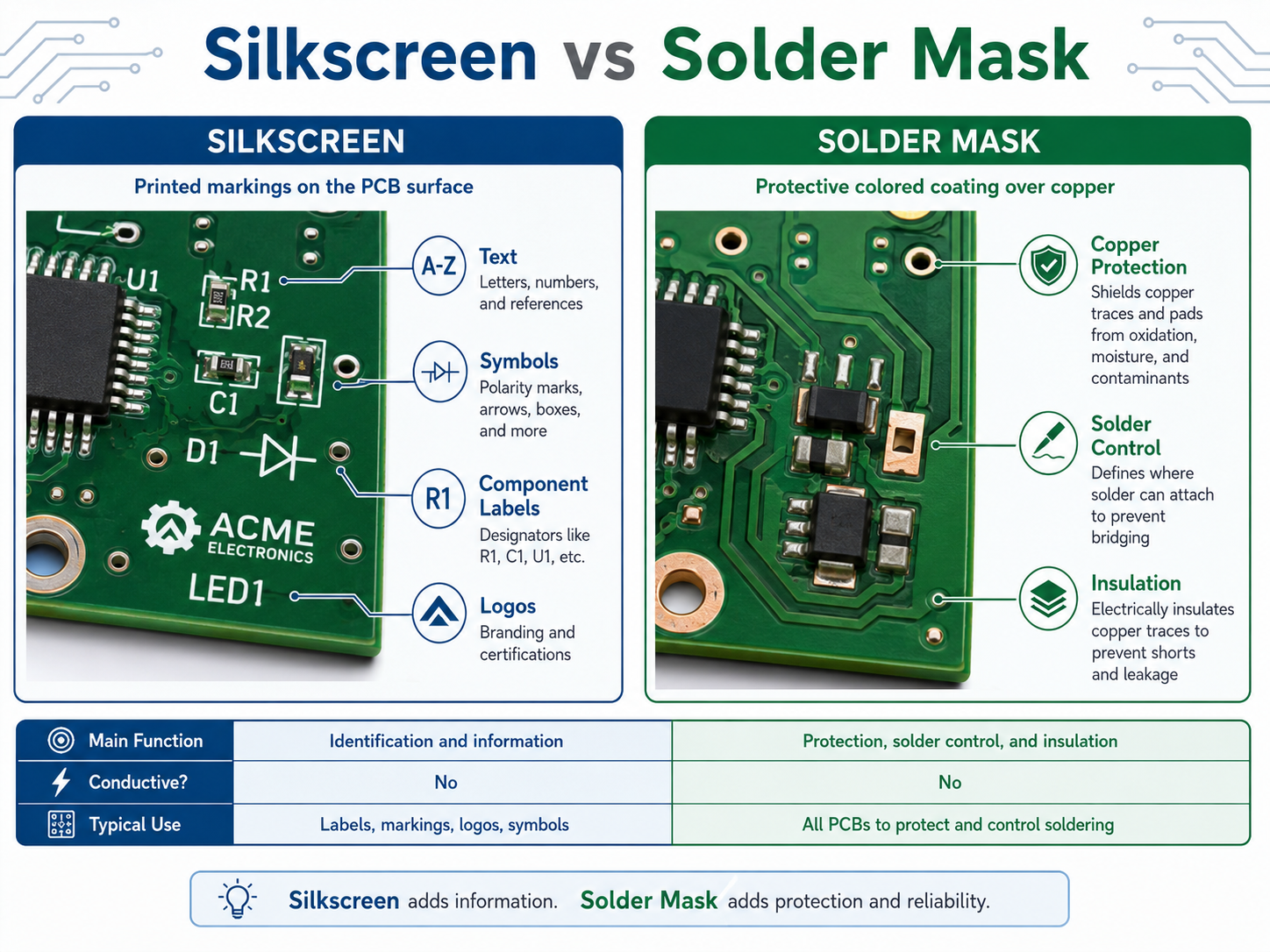
5. What is the difference between PCB silkscreen and solder mask?
Solder mask is the protective coating that covers copper and helps control soldering areas. Silkscreen is the printed legend layer that shows text, symbols, component labels, and other readable information. Solder mask affects insulation and solderability. Silkscreen mainly supports assembly, inspection, testing, and maintenance. They are separate layers in PCB manufacturing files.
6. What information should never be missing from PCB silkscreen?
The most important markings are pin-1 indicators, polarity marks, connector labels, key test point labels, revision identification, and safety warnings. For regulated or controlled products, compliance and traceability marks may also be required. Decorative logos are less important. If board space is limited, prioritize markings that prevent wrong assembly, wrong wiring, wrong testing, or traceability confusion.
7. What is the best silkscreen color for PCB readability?
White silkscreen is the most common choice for green, red, blue, black, and purple solder mask. Black silkscreen is often used on white solder mask. The best color depends on contrast, surface finish, lighting, coating, and customer appearance requirements. For industrial boards, readability is more important than decoration. Always confirm the solder mask and ink combination before production.
8. Should reference designators be printed for every component?
Not always. On dense SMT boards, printing every reference designator can make the silkscreen crowded and unreadable. It is better to prioritize critical parts, connectors, ICs, test points, and polarized components. For very compact boards, reference designators can be moved to an assembly drawing. The goal is not to print more text. The goal is to provide useful production guidance.
9. What should I do if I receive PCBs with missing silkscreen?
Compare the received boards with the approved Gerber files, fabrication drawing, and purchase order requirements. Identify whether the missing information is cosmetic, assembly-related, traceability-related, or compliance-related. If it affects polarity, pin 1, safety, revision control, or required marking, contact the supplier immediately. For urgent prototypes, you may accept with added documentation. For production, request corrective action.
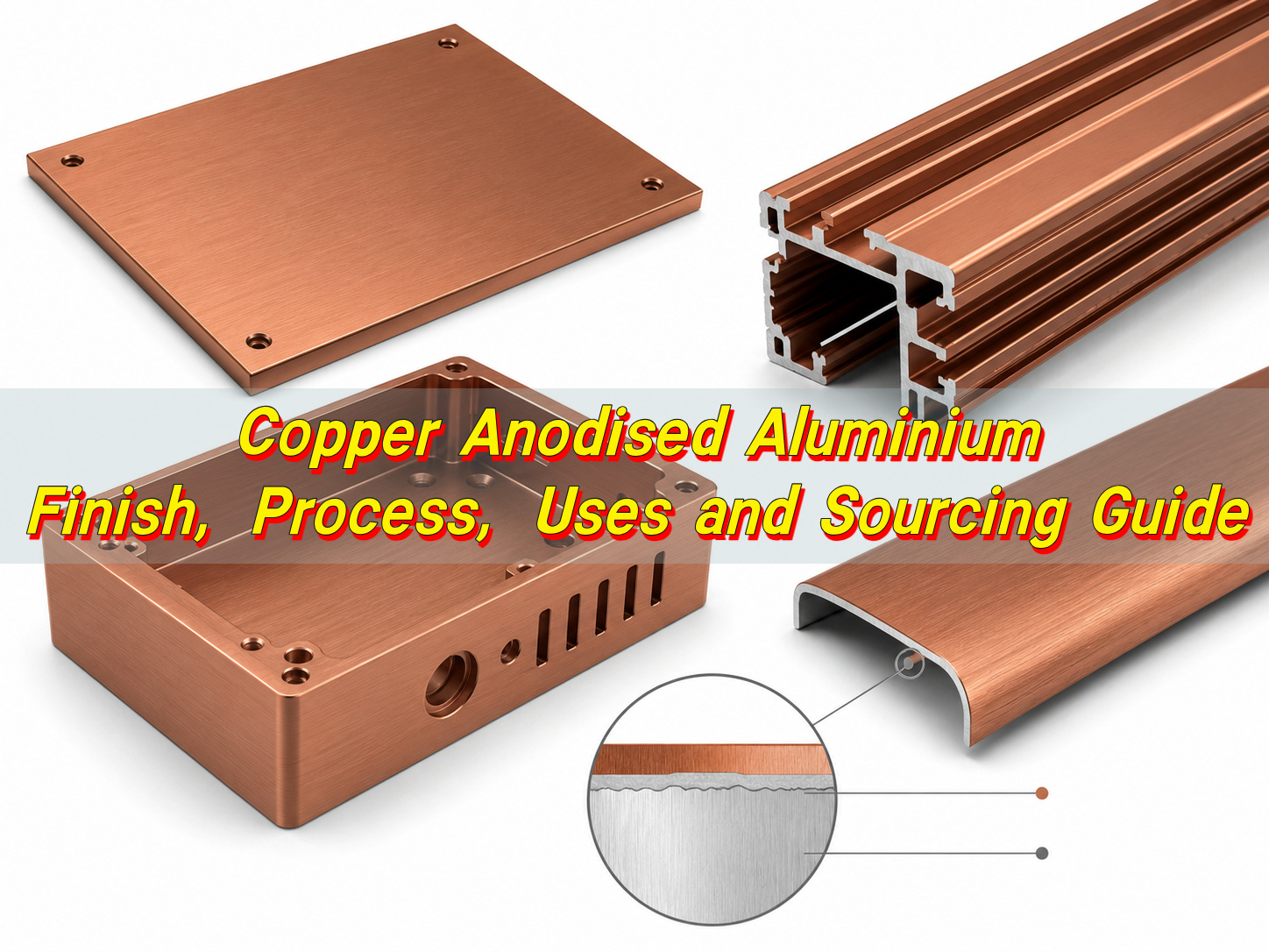
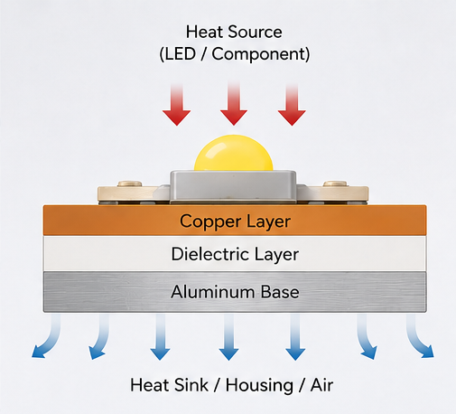
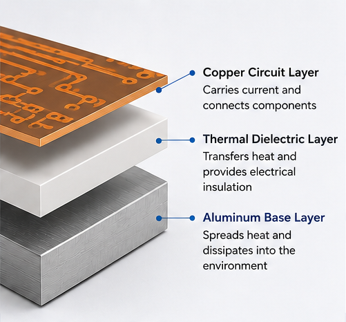
Copper anodised aluminium gives aluminium parts a warm copper-like appearance while keeping the light weight, corrosion resistance, and design flexibility of anodised aluminium. In most engineering and architectural sourcing contexts, this term refers to aluminium that has been anodised and coloured to look like copper, not pure copper that has been anodised. That distinction matters. If your project needs copper’s electrical or thermal conductivity, you may need copper, copper plating, copper-clad aluminium, or another conductive structure. If your project needs a durable copper-tone surface on lightweight aluminium, copper anodised aluminium is often a practical choice.
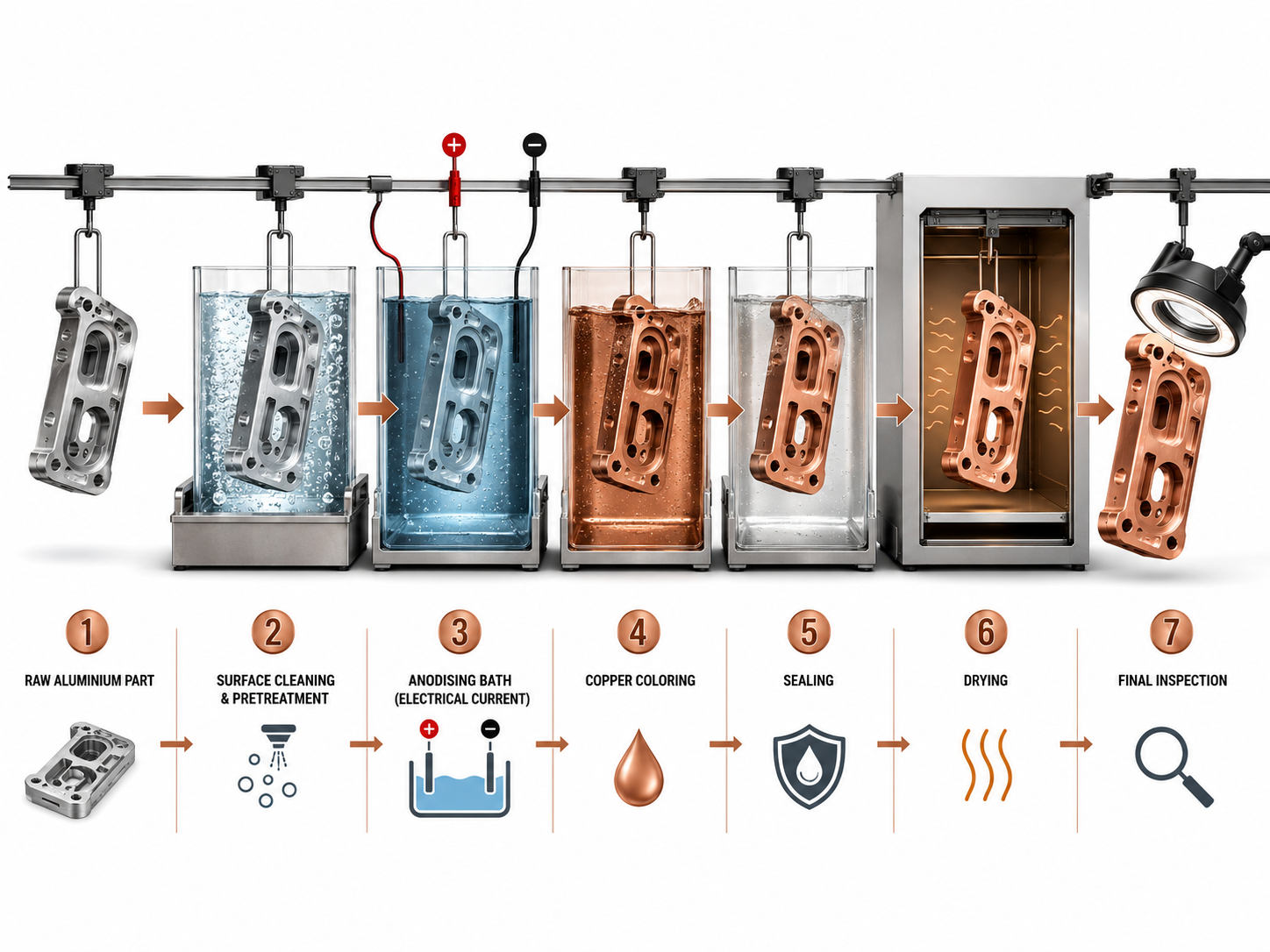
What Is Copper Anodised Aluminium?
Copper anodised aluminium is aluminium that has gone through an electrochemical anodising process and then received a copper-coloured finish. The base material remains aluminium. The surface becomes an aluminium oxide layer that is harder and more corrosion-resistant than untreated aluminium.
The word “copper” usually describes the colour effect. It may look like brushed copper, satin copper, bronze-copper, rose copper, or darker architectural copper. The exact appearance depends on alloy grade, surface pretreatment, anodising thickness, colouring method, sealing quality, and viewing angle.
This finish is popular because it creates a premium metallic appearance without the weight, patina behaviour, and cost structure of solid copper. It is used for architectural trim, decorative panels, electronic housings, lighting parts, furniture hardware, industrial nameplates, control panels, and custom OEM aluminium components.
Anodising is widely used to thicken the natural oxide layer on aluminium and improve corrosion resistance, wear resistance, colour retention, and surface stability. ISO 7599:2018 also defines requirements and test methods for decorative and protective anodic oxidation coatings on aluminium and aluminium alloys.
Why Is Copper Anodised Aluminium Important?
Copper anodised aluminium solves a common design problem: many products need the visual warmth of copper, but pure copper is heavy, costly, reactive, and not always easy to maintain. Aluminium is lighter and easier to machine, extrude, bend, stamp, and assemble. When anodised properly, it can offer a durable decorative surface with a refined metallic texture.
For designers, the value is appearance and material efficiency. A product can look premium without using solid copper. For engineers, the value is surface protection, dimensional control, and repeatable production. For buyers, the value is stable cost, lower part weight, and better suitability for volume manufacturing.
In overseas B2B procurement, this finish is especially useful when brands want consistent colour across batches. Natural copper develops patina over time. Copper anodised aluminium can be specified to maintain a more controlled copper-tone appearance, depending on the anodising system and exposure environment.
How Does Copper Anodised Aluminium Work?
The anodising process turns the aluminium surface into a controlled aluminium oxide layer. The aluminium workpiece acts as the anode in an electrolytic bath. Under controlled current, temperature, and chemistry, the oxide layer grows from the surface. This layer is not a paint film sitting on top of the metal. It is integrated with the aluminium substrate, which helps improve durability.
A typical process flow includes cleaning, alkaline etching, desmutting, anodising, colouring, sealing, drying, and inspection. For copper-coloured finishes, the colouring stage is critical. The manufacturer may use organic dyes, electrolytic colouring, or proprietary colouring systems to create the copper tone. After colouring, sealing closes the pores in the anodic coating and helps improve corrosion resistance, stain resistance, and colour stability.
The process must be controlled carefully. Small changes in alloy, surface texture, bath temperature, film thickness, dye concentration, sealing time, or rack position can affect the final colour. That is why professional production usually requires approved limit samples before bulk orders.
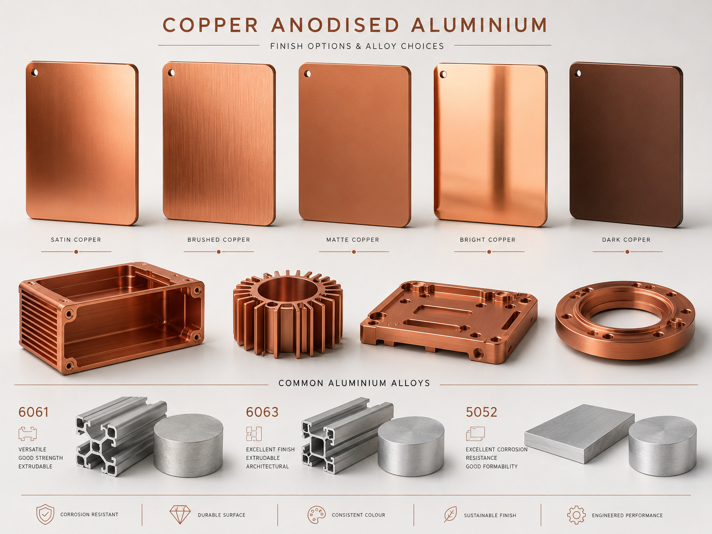
What Types of Copper Anodised Aluminium Are Available?
Copper anodised aluminium is not one single finish. It can be adjusted by colour depth, surface texture, gloss level, coating thickness, and performance requirement.
Type
Typical Appearance
Common Use
Key Buying Note
Satin copper anodised aluminium
Soft brushed copper tone
Electronic housings, panels, trim
Good balance of appearance and fingerprint control
Bright copper anodised aluminium
More reflective metallic copper
Decorative parts, consumer products
Surface defects are easier to see
Matte copper anodised aluminium
Low-gloss industrial copper tone
Machinery panels, signage, architectural details
More forgiving for visual consistency
Dark copper anodised aluminium
Copper-bronze or antique copper effect
Façade parts, furniture, lighting
Needs strict colour sample control
Hard anodised copper-tone aluminium
Thicker, more wear-focused coating
Industrial components
Decorative colour choices may be more limited
Brushed copper anodised aluminium
Linear grain texture
Door trim, instrument panels, premium devices
Grain direction must be specified
For decorative parts, Type II sulphuric acid anodising is common because it can accept colour well. For wear-focused parts, Type III hard anodising may be selected, but colour options can be less predictable. MIL-PRF-8625 covers different anodic coating types and classes for aluminium and aluminium alloys, including dyed and non-dyed classes for non-architectural applications.
Which Materials Are Suitable for Copper Anodised Aluminium?
Not all aluminium grades anodise the same way. The alloy strongly affects colour consistency, brightness, corrosion resistance, and surface texture. For visible copper-tone anodised parts, 5xxx and 6xxx series aluminium alloys are often easier to manage than high-copper or high-silicon alloys.
Aluminium Alloy
Anodising Suitability
Typical Applications
Notes
6063
Excellent for decorative anodising
Extrusions, frames, trims
Often preferred for architectural profiles
6061
Good general-purpose option
CNC parts, housings, brackets
Stable strength and machinability
5052
Good corrosion resistance
Panels, sheet metal covers
Common for formed sheet parts
6082
Good mechanical strength
Structural machined parts
Colour may need sample confirmation
7075
More difficult for decorative consistency
High-strength parts
Colour can appear darker or less uniform
2xxx series
Usually challenging
Aerospace and high-strength parts
Copper content may affect anodising appearance
For high-appearance projects, do not choose the alloy only by mechanical strength. Choose it by both mechanical requirement and anodising response. A part that performs well mechanically may still produce a poor copper colour after anodising.
What Are the Key Features of Copper Anodised Aluminium?
Copper anodised aluminium offers a mix of decorative and functional features. The most important feature is that it gives aluminium a copper-like surface while keeping the base metal lightweight. It also improves surface hardness compared with untreated aluminium and provides better protection against oxidation and environmental exposure.
Another key feature is colour flexibility. The copper tone can be tuned from light rose-copper to deeper bronze-copper. Surface preparation can also change the final result. A brushed surface creates a different visual effect from a bead-blasted or polished surface.
The anodic layer is electrically insulating. This is useful in some products, but it can create grounding problems in electronic assemblies. If the aluminium part must provide electrical continuity, the drawing should clearly define masked areas, conductive contact points, threaded grounding locations, or post-machined contact surfaces.
What Are the Advantages of Copper Anodised Aluminium?
The main advantage is appearance-to-weight efficiency. Solid copper is much heavier than aluminium. Aluminium can reduce product weight while still giving a copper-style visual effect. This is useful for wall panels, enclosures, lighting products, handles, display frames, and portable devices.
Another advantage is controlled surface performance. Unlike paint, anodising becomes part of the aluminium surface. It is less likely to chip like a coating film. With proper sealing, it can resist staining and everyday handling better than raw aluminium.
It also supports volume manufacturing. Aluminium can be extruded, CNC machined, stamped, laser cut, bent, drilled, tapped, and assembled before anodising. This makes it suitable for OEM and ODM projects where the buyer needs both custom geometry and a controlled decorative surface.
For architectural aluminium, high-performance exterior anodised finishes are often specified according to AAMA 611 Class I requirements, especially when long-term outdoor durability, UV exposure, salt spray resistance, and abrasion performance are important.
What Are the Limitations of Copper Anodised Aluminium?
The first limitation is colour tolerance. Copper anodised aluminium is sensitive to alloy batch, surface pretreatment, anodising thickness, sealing, and viewing light. Even if two parts use the same dye, they may not look identical if the alloy or surface finish changes.
The second limitation is repair difficulty. Scratches that cut through the anodic layer are not easy to repair invisibly. Small surface marks may require rework or full refinishing. For visible consumer or architectural parts, packaging and handling are part of the quality plan, not an afterthought.
The third limitation is conductivity. Anodised aluminium has an insulating oxide layer. For electronic enclosures, heat sinks, grounding plates, or shielded housings, the manufacturer must reserve conductive areas where needed.
The fourth limitation is outdoor colour stability. Some colour systems are more suitable for indoor products, while others are designed for exterior architectural use. If the product will face sunlight, humidity, salt mist, or industrial air pollution, the buyer should specify the exposure environment before quotation.
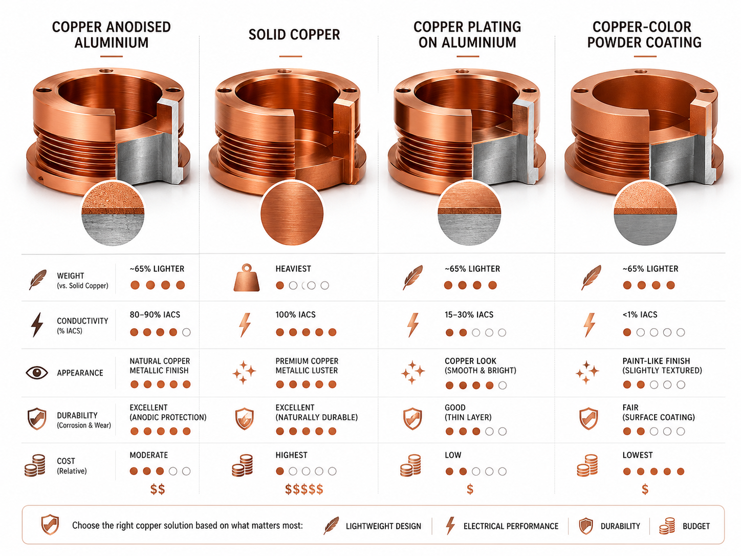
How Does Copper Anodised Aluminium Compare With Other Copper-Look Finishes?
Different copper-look finishes serve different goals. Copper anodised aluminium is not always the best solution, but it is often the best balance when the project needs a durable metallic look on an aluminium base.
Finish Option
Main Benefit
Main Concern
Best Fit
Copper anodised aluminium
Lightweight, metallic appearance, good durability
Colour control must be managed
Decorative aluminium parts and panels
Solid copper
Real copper conductivity and natural patina
Heavy, costly, changes colour over time
Electrical, heritage, premium metalwork
Copper plating on aluminium
Real copper surface layer
Adhesion and corrosion control are critical
Conductive or decorative plated parts
Powder-coated copper colour
Broad colour options and lower visual tolerance risk
Less metallic depth than anodising
Large panels, cost-sensitive projects
PVD copper coating
Premium appearance, thin hard coating
Higher cost and process limitation
Luxury hardware, small precision parts
Copper-colour paint
Easy colour matching
Lower scratch resistance
Low-cost decorative parts
If your priority is electrical conductivity, copper anodised aluminium is usually not the right answer. If your priority is copper appearance, aluminium weight, and anodised surface durability, it can be a strong option.
How Should Engineers Choose the Right Specification?
A good specification should describe more than “copper anodised aluminium.” That phrase is too broad for production. Engineers should define the alloy, temper, surface texture, anodising type, coating thickness, colour target, gloss range, sealing method, masking areas, inspection method, and packing requirement.
A practical drawing note may include the aluminium grade, such as 6061-T6 or 6063-T5, followed by the required anodising type and finish colour. For example, a decorative enclosure may call for satin copper anodised finish with approved colour sample, coating thickness range, sealed surface, and masked grounding points.
For high-appearance projects, approved samples are essential. One “golden sample” is useful, but limit samples are better. Limit samples show the acceptable light, medium, and dark colour range. This helps reduce disputes during mass production.
For assembled products, engineers should also consider tolerance change. Anodising creates a surface layer that changes dimensions slightly. Threads, press-fit holes, tight sliding surfaces, and cosmetic edges should be reviewed before production.
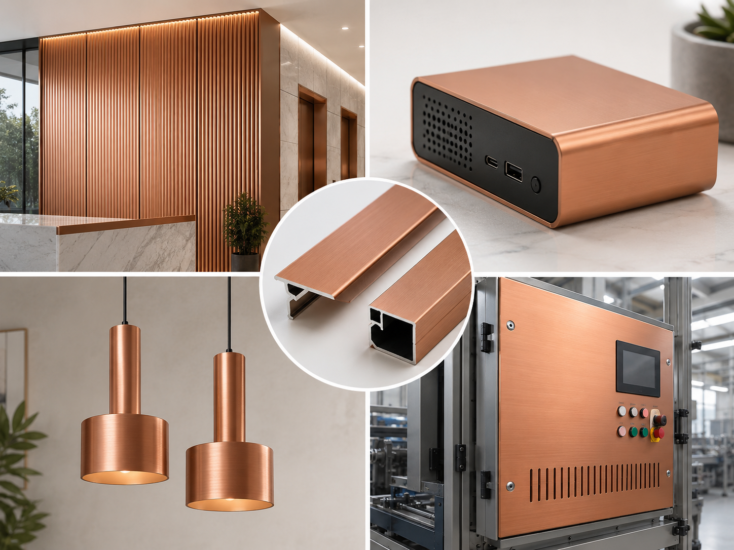
Where Is Copper Anodised Aluminium Used?
Copper anodised aluminium is used wherever design teams want a warm metal appearance with lightweight aluminium performance. It appears in architecture, electronics, lighting, retail displays, furniture, transportation interiors, industrial equipment, and premium consumer products.
In architecture, it is used for curtain wall trims, door frames, ceiling profiles, decorative panels, elevator interiors, and signage. In electronics, it is used for aluminium enclosures, faceplates, control panels, amplifier housings, router shells, and instrument covers. In lighting, it is used for lamp bodies, reflectors, pendant housings, and decorative heat-dissipation structures.
For industrial equipment, the finish can be used on operator panels, machine covers, identification plates, knobs, handles, brackets, and exposed mechanical parts. For consumer products, it can support a premium copper-tone design without making the product too heavy.
What Practical Cases Show Its Value?
A lighting manufacturer may choose brushed copper anodised aluminium for pendant lamp housings. The aluminium body supports heat dissipation and weight reduction, while the copper-tone surface creates a warm interior design style. The key production risk is colour difference between spun, extruded, and machined parts, so all parts should use aligned pretreatment and approved colour limits.
An electronics brand may use copper anodised aluminium for a CNC-machined audio amplifier enclosure. The buyer wants a premium surface, clean edges, and stable colour. The engineering team should reserve un-anodised grounding points inside the enclosure and protect threaded holes where electrical bonding is required.
An architectural supplier may use dark copper anodised aluminium profiles for interior wall trims. The priority is batch consistency across long profiles. The supplier should control extrusion source, surface grain direction, anodising load, sealing, and packaging to avoid visible shade bands on installed walls.
A machinery manufacturer may use matte copper anodised aluminium nameplates and control panels. The finish improves appearance and surface protection, while laser engraving or screen printing can add durable markings. The buyer should test ink adhesion, engraving contrast, and cleaning resistance before batch order.
What Should Designers Consider Before Production?
Designers should start with the final environment. Indoor decorative parts have different requirements from outdoor building components or industrial equipment near chemicals. For outdoor use, weather resistance, UV exposure, salt mist, and cleaning chemicals must be discussed early.
Surface texture should be locked before colour approval. Brushing, polishing, sandblasting, bead blasting, and chemical etching all change how copper colour appears. Even the same anodising bath can look different on different textures.
Designers should avoid sharp edges where possible. Very sharp corners can anodise unevenly and become weak points for scratches. Radiused edges usually improve both appearance and handling durability.
Assemblies also need attention. If copper anodised aluminium parts are assembled with stainless steel screws, plastic clips, rubber pads, adhesives, or gaskets, the contact points should be tested. Friction during assembly can create scratches, pressure marks, or colour damage.
How Is Copper Anodised Aluminium Manufactured and Tested?
Manufacturing begins with stable raw material. The supplier checks alloy grade, surface condition, thickness, and mechanical processing requirements. After machining or forming, the parts are cleaned to remove oil, fingerprints, cutting fluid, and oxide contamination.
Pretreatment shapes the final appearance. Alkaline etching creates a matte surface. Mechanical brushing creates directional grain. Polishing increases brightness. After pretreatment, anodising builds the oxide layer. Colouring gives the copper tone. Sealing improves surface stability.
Testing should match the product’s risk level. Cosmetic indoor parts may need visual inspection, colour comparison, coating thickness check, and packaging review. Outdoor or industrial parts may need salt spray testing, abrasion testing, seal quality testing, UV resistance evaluation, and chemical resistance checks.
Quality Item
Why It Matters
Common Control Method
Alloy verification
Prevents colour and performance variation
Material certificate, incoming inspection
Surface pretreatment
Controls texture and reflectivity
Sample approval, visual standard
Coating thickness
Affects durability and dimensions
Eddy current thickness measurement
Colour consistency
Prevents visible batch mismatch
Limit samples, colour meter, controlled lighting
Sealing quality
Improves stain and corrosion resistance
Dye spot, admittance, or mass-loss methods
Masking accuracy
Protects conductive or assembly areas
Fixture review and visual inspection
Scratch protection
Maintains cosmetic grade
Film, foam, tray, or individual packing
ISO 2143 specifies a dye absorption method for checking sealed anodic oxidation coatings, especially where staining resistance or weather exposure is important.
What Failures Can Happen and How Can They Be Prevented?
Colour mismatch is one of the most common failures. It often comes from mixed alloy batches, uneven pretreatment, different surface roughness, or unstable anodising parameters. The solution is to control alloy source, use approved limit samples, and avoid mixing different material batches in one visible assembly.
Fading can happen when the colour system is not suitable for the application environment. For exterior parts, the buyer should ask about lightfastness, sealing method, and outdoor test data. For indoor parts exposed to strong sunlight, UV resistance still matters.
White spots or stains may come from poor cleaning, poor sealing, trapped chemicals, or contaminated rinse water. Better rinsing, stable sealing, and clean packaging help reduce this risk.
Pitting and corrosion may appear when the wrong alloy is used or when pretreatment exposes inclusions. This is more likely on low-quality raw material or parts used in marine and industrial environments.
Rack marks are another practical issue. Anodising requires electrical contact. The supplier should define rack locations before production, especially for visible parts.
Thread and fit problems can happen when anodising thickness is not considered. Critical holes, threads, sliding features, and press-fit areas may need masking or post-machining.
What Affects the Cost of Copper Anodised Aluminium?
The cost depends on raw material, part size, alloy grade, surface finish, anodising type, colour difficulty, tolerance, inspection level, order quantity, packaging, and logistics. Bright finishes usually need better raw material and more surface preparation. Dark copper shades may require tighter colour control. Long profiles need stable anodising tanks and careful handling.
Small orders often have higher unit costs because colour adjustment, racking, sampling, and process setup still take time. Bulk production can reduce unit cost, but only if the specification is stable.
Complex parts cost more when they need masking, two-sided cosmetic control, hidden rack positions, tight holes, or special packing. If the part has both cosmetic and functional requirements, such as an anodised housing with grounding points, the supplier must add process controls.
For global buyers sourcing from a China-based manufacturer, total landed cost should include tooling, samples, surface approval, packaging, freight, duty, inspection, and possible rework risk. A low surface-finishing quotation is not always lower cost if colour consistency and packing are weak.
How Can Buyers Choose a Reliable Supplier?
A reliable supplier should understand both aluminium manufacturing and anodising control. The buyer should ask whether the supplier can support CNC machining, extrusion, sheet metal fabrication, brushing, polishing, anodising, inspection, assembly, and export packing. For OEM and ODM projects, this integrated capability can reduce handover errors.
The supplier should be able to discuss alloy selection, surface pretreatment, coating thickness, masking, colour tolerance, and inspection methods before quoting. If a supplier only quotes by part weight or surface area without asking about appearance level, the project may carry hidden risk.
Buyers should request sample approval before mass production. For visible parts, limit samples are better than one perfect sample. For outdoor products, buyers should ask for the applicable standard, test method, and expected exposure environment.
A China source factory can be a strong option for custom copper anodised aluminium parts when the project needs flexible manufacturing, controlled batch production, and global shipment. The key is not to claim false local production. The real advantage is engineering communication, process integration, cost control, and stable export support.
What Should Be Checked Before Placing an Order?
Before placing an order, the buyer should check the full technical package. The drawing should include material grade, temper, dimensions, tolerance, surface finish, anodising type, copper colour requirement, coating thickness, sealing requirement, masking areas, visible surface definition, inspection standard, and packaging method.
The buyer should also confirm whether the part is for indoor or outdoor use. Outdoor architectural parts need stronger durability requirements than indoor decorative covers. Electronics housings may need conductive contact points. Lighting parts may need thermal and surface testing. Industrial panels may need chemical cleaning resistance.
A pre-production checklist can prevent most disputes:
Checkpoint
Recommended Requirement
Colour
Approved golden sample and light/dark limit samples
Surface texture
Brushed, polished, matte, blasted, or custom texture defined
Alloy
Same alloy and batch control for visible assemblies
Thickness
Coating thickness range specified
Conductivity
Masked grounding or contact areas marked
Assembly
Screw holes, clips, adhesives, and gasket contact tested
Environment
Indoor, outdoor, marine, industrial, or high-UV use confirmed
Packaging
Scratch-proof packing and handling method approved
This step is especially important for export orders. Once parts are shipped internationally, rework becomes expensive and slow.
Frequently Asked Questions About Copper Anodised Aluminium
Is copper anodised aluminium real copper?
Usually, no. It is normally aluminium that has been anodised and coloured to look like copper. The base metal is still aluminium. If your design needs copper’s electrical conductivity, antimicrobial behaviour, or natural patina, you should consider solid copper, copper plating, or copper-clad material instead.
Does copper anodised aluminium turn green like copper?
A properly anodised copper-coloured aluminium finish does not develop natural green copper patina in the same way as real copper. The surface is aluminium oxide with colour treatment. However, poor sealing, harsh chemicals, UV exposure, or unsuitable dye systems may still cause fading, staining, or colour change.
Can copper anodised aluminium be used outdoors?
Yes, but the specification must match the environment. Outdoor use requires better sealing, weather-resistant colour systems, suitable alloy selection, and proper testing. For architectural projects, buyers often consider recognised exterior aluminium finishing requirements and request durability evidence before approving bulk production.
What aluminium alloy is best for copper anodising?
6063 is often preferred for decorative extrusions, while 6061 is widely used for CNC parts and housings. 5052 is useful for sheet metal panels. High-copper or high-silicon alloys can be harder to colour consistently, so sample testing is important before production.
Is copper anodised aluminium conductive?
The aluminium core is conductive, but the anodised surface layer is electrically insulating. If the part needs grounding, EMI shielding, or electrical contact, the drawing should define masked areas, conductive contact pads, tapped grounding holes, or post-machined contact surfaces.
Can the copper colour be perfectly matched every time?
Perfect matching is difficult because anodising colour depends on alloy, surface texture, film thickness, bath control, sealing, and lighting. Professional suppliers manage this with approved colour samples, limit samples, controlled material batches, and consistent pretreatment.
What is the difference between copper anodised aluminium and copper plating?
Copper anodised aluminium has a coloured anodic oxide layer on aluminium. Copper plating deposits a real copper layer onto the surface. Anodising is often chosen for decorative durability on aluminium, while copper plating is chosen when a real copper surface or conductivity is required.
Can scratched copper anodised aluminium be repaired?
Minor surface marks may sometimes be polished or hidden, but deep scratches that cut through the anodised layer are difficult to repair invisibly. Visible parts should use protective film, careful handling, soft separators, and scratch-resistant packaging during production and shipping.
Is hard anodising available in copper colour?
Sometimes, but colour control can be more limited than decorative Type II anodising. Hard anodising is mainly selected for wear resistance and thicker coatings. If both strong wear resistance and copper appearance are required, sample validation is essential.
Why does copper anodised aluminium show colour difference between parts?
Colour variation may come from different alloy batches, different surface roughness, uneven etching, film thickness variation, poor dye control, inconsistent sealing, or mixed production loads. For assemblies, all visible parts should be processed under the same controlled conditions when possible.
What surface finish looks best with copper anodising?
Brushed and satin finishes are popular because they create a premium metallic look and hide minor handling marks better than mirror-bright surfaces. Matte blasted surfaces give a softer industrial look. Bright finishes can look attractive but require better raw material and stricter defect control.
What should buyers send for quotation?
Buyers should send 2D drawings, 3D files, alloy requirement, quantity, surface texture, copper colour target, coating thickness, application environment, visible surface definition, masking areas, and packing requirement. If possible, send a reference sample or colour target to reduce misunderstanding.
Is copper anodised aluminium suitable for electronic enclosures?
Yes, it is commonly used for electronic housings, audio equipment, control panels, and instrument covers. The key is to reserve conductive areas for grounding and assembly. Engineers should also check heat dissipation, thread tolerance, screw contact, and cosmetic protection.
How can buyers reduce cost without lowering quality?
Choose an anodising-friendly alloy, avoid unnecessary mirror polishing, define realistic colour tolerance, approve limit samples, combine similar parts in one production batch, and simplify masking where possible. Clear drawings and stable specifications help reduce sampling time, rework, and inspection disputes.
Conclusion:
Copper anodised aluminium is a practical finish for projects that need copper-like appearance, aluminium weight advantage, corrosion resistance, and scalable production. The most important technical point is simple: it is usually copper-coloured anodised aluminium, not anodised copper. This distinction helps engineers avoid wrong material decisions, especially in projects involving grounding, conductivity, thermal design, or outdoor exposure.
For selection, start with alloy, surface texture, anodising type, coating thickness, colour tolerance, sealing quality, and application environment. For procurement, ask for approved samples, limit samples, inspection methods, packing details, and clear communication about visible surfaces.
PCB missing silk screen means part or all of the printed legend layer is absent, unclear, clipped, misaligned, or unreadable on the finished circuit board. It may not always affect electrical function, but it can influence PCB assembly, polarity identification, inspection, traceability, and field maintenance.
What Does PCB Missing Silk Screen Mean?
PCB missing silk screen means that the printed marking layer on the board is incomplete or not visible. This may include missing component reference designators, polarity marks, logos, pin-1 indicators, connector labels, test point names, warning marks, or revision codes.
In PCB manufacturing, the silk screen layer is also called the legend layer or nomenclature layer. It is usually printed in white, black, yellow, or another readable ink color on top of the solder mask. Its main role is not electrical conduction. Instead, it supports assembly, inspection, repair, traceability, and product identification.
A missing silkscreen on PCB does not always mean the circuit board is electrically defective. Many boards can still function normally without printed legend. However, for assembly, testing, field maintenance, regulated products, and high-mix production, missing silk screen can create practical risks.
Why Is Silk Screen Important on a PCB?
Silk screen is important because it turns a bare PCB into a readable manufacturing and service reference. It helps operators, inspectors, engineers, and end users understand the board layout quickly.
In PCB assembly, reference designators such as R12, C8, U3, D5, J1, and TP6 help operators match components to the correct locations. Polarity marks help identify the orientation of diodes, electrolytic capacitors, LEDs, ICs, connectors, and batteries. Test point names help engineers debug signals during functional testing.
Silk Screen Information
Practical Use
Component reference designators
Helps assembly, inspection, and troubleshooting
Polarity marks
Prevents orientation errors for polarized parts
Pin-1 marks
Supports correct IC and connector placement
Test point labels
Speeds up electrical testing and repair
Revision code
Helps distinguish PCB versions
Logo and part number
Supports product identification
Warning marks
Improves safety for high-voltage or power boards
Connector labels
Helps cable installation and field maintenance
Common Types of PCB Missing Silk Screen Problems
PCB missing silk screen can appear in several forms. Each type usually points to a different design, CAM, or manufacturing issue.
Problem Type
What It Looks Like
Common Meaning
Entire silk screen missing
No text, logo, or marking on the board
Legend Gerber layer missing or not selected
Partial silk screen missing
Some labels visible, some absent
CAM clipping, solder mask conflict, or design issue
Text too faint
Legend exists but is hard to read
Ink thickness, curing, contrast, or surface issue
Misaligned silk screen
Text shifted from the correct position
Registration error during printing
Silk screen covered by components
Labels hidden after assembly
Layout placement issue
Silk screen printed on pads
Ink appears on exposed copper or solderable area
Poor DFM control or missing clearance
Broken characters
Text appears incomplete or fragmented
Line width too small or resolution limit
Missing polarity marks
Diode, LED, capacitor, or IC marks absent
Library or Gerber export error
What Causes Missing Silk Screen on PCB?
PCB missing silk screen usually comes from design file issues, CAM processing, manufacturing capability limits, or production process control. The exact cause should be checked from Gerber data, fabrication notes, production records, and finished board inspection.
Cause
Explanation
Prevention
Legend layer not included
The top or bottom silk screen file was not exported
Check the Gerber package before release
Wrong layer name
CAM may not identify the legend layer correctly
Use clear layer naming such as GTO and GBO
Silk screen overlaps pads
Manufacturer removes markings from solderable areas
Keep proper clearance from pads
Text line width too small
Fine text may disappear during printing
Follow minimum legend width rules
Text height too small
Tiny characters become unreadable
Use practical text size for production
Poor ink contrast
Ink color and solder mask color are too similar
Choose readable color combinations
Solder mask expansion issue
Legend is clipped by mask opening rules
Run DFM before fabrication
Printing registration error
Legend shifts during production
Control alignment and process tolerance
File conversion issue
DXF, ODB++, Gerber, or CAD export causes missing data
Review generated manufacturing files
Customer intentionally removed it
Some high-density or cosmetic boards omit silk screen
Confirm drawing and acceptance criteria
Is Missing Silk Screen a Functional Defect?
Missing silk screen is usually not an electrical defect by itself. The copper circuits, solder mask, drilling, plating, impedance, and surface finish decide electrical performance. However, missing silk screen can become a manufacturing or quality risk when it affects assembly, inspection, test, traceability, or product use.
Application Situation
Risk Level
Recommended Action
Simple prototype board
Low to medium
Confirm with engineer before use
Dense SMT assembly
Medium
Check assembly drawings and polarity marks
Power electronics
Medium to high
Verify warning marks and polarity
Medical electronics
High
Confirm traceability and documentation needs
Automotive electronics
High
Check revision control and inspection records
Aerospace or UAV boards
High
Review all markings and quality documents
Field-serviceable equipment
High
Ensure connectors and test points are readable
How to Check PCB Missing Silk Screen Before Manufacturing
The best time to find missing silk screen is before PCB fabrication. Once boards are manufactured, correction becomes slower and more expensive.
Before releasing files, engineers should check the PCB legend layer in a Gerber viewer, not only in the PCB design software. CAD view and manufacturing output are not always identical.
Check Item
What to Confirm
Top silk screen layer
GTO or top legend file is included
Bottom silk screen layer
GBO or bottom legend file is included if needed
Text visibility
Reference designators and marks are readable
Text height and width
Characters meet manufacturer capability
Pad clearance
Ink does not touch solder pads or exposed copper
Polarity marks
Diodes, LEDs, ICs, capacitors, and connectors are marked
Revision and part number
Correct PCB version is printed
Logo or customer marking
Included only if approved
Board outline relation
Text is not outside the final board edge
Assembly readability
Markings are still useful after components are mounted
How Manufacturers Handle Silk Screen During PCB Fabrication
During PCB fabrication, the manufacturer reviews the legend layer during CAM processing. If silk screen overlaps pads, vias, solder mask openings, castellated holes, gold fingers, edge contacts, or test points, the CAM team may clip or remove those parts to protect solderability.
This is why some customers see missing silk screen even though the original design file included it. The legend may have been removed because it violated production rules.
Manufacturing Step
Silk Screen Control Point
CAM review
Confirms legend layer, clearance, readability, and conflicts
Solder mask process
Defines openings where ink should not be printed
Legend printing
Applies ink by screen printing or inkjet printing
Curing
Hardens legend ink for adhesion and durability
Visual inspection
Checks readability, alignment, and missing areas
Final QC
Compares finished board with approved Gerber or drawing
Can Missing Silk Screen Be Reworked?
Missing silk screen can sometimes be reworked, but feasibility depends on board type, quantity, required appearance, and acceptance standard.
For a small prototype batch, manual marking, label stickers, or controlled reprinting may be acceptable. For mass production or customer-facing products, rework must be handled carefully because uneven marking can affect appearance, traceability, and process consistency.
Rework Method
Suitable For
Limitation
Manual marking
Engineering samples or internal prototypes
Not ideal for mass production
Adhesive labels
Box-build or internal identification
May not survive heat, solvents, or cleaning
Local reprint
Partial correction on selected areas
Requires process control and alignment
Full remake
Critical production boards
Higher cost but best consistency
Accept as-is
Non-critical missing legend
Requires written customer approval
Design Rules to Prevent PCB Missing Silk Screen
Good legend design starts in the PCB layout stage. The goal is not to print every possible label. The goal is to print the right information in a readable and manufacturable way.
Design Rule
Practical Recommendation
Keep text readable
Avoid extremely small characters
Use enough line width
Prevent broken or faint letters
Avoid pads and exposed copper
Keep legend away from solderable areas
Prioritize key marks
Keep polarity, pin-1, connector, and test point marks
Use clear orientation symbols
Mark diodes, LEDs, ICs, and electrolytic capacitors clearly
Avoid component body overlap
Place text where it remains visible after assembly
Confirm board side
Do not confuse top and bottom legend layers
Use consistent naming
Match BOM, assembly drawing, and PCB layout
Add revision marking
Support version control in production
Review final Gerber
Check output files, not only CAD layout
How Missing Silk Screen Affects PCB Assembly
Missing silk screen can slow down PCB assembly because operators and inspectors need additional documents to confirm component placement. Automated SMT machines use centroid files, BOM, and programming data, so they do not rely only on legend. However, human inspection, first article inspection, repair, and debugging still benefit from clear markings.
Assembly Stage
Possible Impact
Incoming board check
Harder to confirm board version
First article inspection
Slower component location verification
Manual component placement
Higher chance of orientation confusion
Through-hole assembly
Connector and polarity checks become slower
AOI review
Inspector may need more document cross-checking
Functional testing
Test point identification takes longer
Debug and repair
Engineers spend more time tracing circuits
Industry Applications Where Silk Screen Quality Matters More
Some PCB applications can tolerate limited legend. Others need clear and stable board marking because production, maintenance, and compliance demands are higher.
Industry
Why Silk Screen Matters
Industrial control
Helps identify terminals, relays, switches, and test points
Medical electronics
Supports traceability, inspection, and controlled production
Automotive electronics
Helps revision control and assembly verification
Aerospace and UAV
Supports documentation, reliability review, and maintenance
Communication equipment
Helps identify RF sections, connectors, and test points
LED lighting
Marks polarity, input/output direction, and thermal zones
Power electronics
Supports high-voltage warnings and connector identification
Consumer electronics
Improves product consistency and assembly communication
Case Study: Solving Missing Silk Screen Before Batch PCB Production
In one production review scenario, a customer submitted a multilayer PCB design for industrial control equipment. The electrical data was complete, but the top legend layer had several clipped reference designators and missing polarity marks near small SMD diodes and connectors.
The problem came from two sources. First, several text labels were placed too close to solder mask openings. Second, some polarity marks used very fine line width, which was below the practical printing capability for stable production.
Before fabrication, the engineering review team corrected the issue by moving critical marks away from pads, enlarging polarity symbols, and keeping connector labels visible after assembly. Non-critical crowded reference designators were left to the assembly drawing instead of forcing unreadable text onto the PCB.
The result was a cleaner board layout, easier first article inspection, and lower risk during assembly. This kind of pre-production correction is often faster than discovering missing silk screen after boards arrive.
What Should Buyers Confirm Before Ordering PCBs?
Buyers should not treat silk screen as a small cosmetic detail only. For prototype and mass production orders, it is better to confirm legend requirements clearly before fabrication.
Buyer Checkpoint
Why It Matters
Confirm whether silk screen is required
Some boards intentionally omit legend
Send complete Gerber files
Prevents missing top or bottom legend layers
Provide assembly drawing
Helps verify key markings
Specify ink color if needed
Improves readability and appearance
Confirm logo and part number
Avoids wrong branding or revision marking
Ask for DFM review
Finds pad overlap and unreadable text early
Request first article photos
Helps verify legend before full production
Define acceptance criteria
Avoids disputes over partial missing marks
Confirm controlled changes
Prevents CAM edits without approval
Keep revision records
Supports future repeat orders
How to Choose a PCB Manufacturer for Better Silk Screen Control
A good PCB manufacturer should not only produce copper circuits correctly. It should also review practical manufacturing details such as legend readability, pad clearance, solder mask opening, version marking, and assembly support.
Supplier Capability
Why It Helps
CAM engineering review
Catches missing or conflicting legend layers
DFM feedback
Helps fix issues before production
Prototype and mass production support
Keeps early samples and batch boards consistent
Visual inspection process
Finds faint, missing, or shifted markings
PCB and PCBA experience
Understands how legend affects assembly
Quality certifications
Supports controlled production systems
Engineering communication
Reduces file interpretation mistakes
Global delivery experience
Helps overseas buyers manage production schedules
EBest Circuit (Best Technology) supports PCB design, PCB prototype, mass production, component sourcing, PCB assembly, and box-build assembly. With experience in FR4 PCB, multilayer PCB, MCPCB, ceramic PCB, flexible PCB, rigid-flex PCB, and high-frequency PCB production, the engineering team can help customers review silk screen risks before fabrication and assembly.
For projects requiring controlled documentation, EBest Circuit (Best Technology) can support quality-oriented production under systems such as ISO 9001, ISO 13485, IATF 16949, AS9100D, UL, RoHS, and REACH-related requirements, based on project scope and customer specifications.
FAQs About PCB Missing Silk Screen
What is PCB missing silk screen?
PCB missing silk screen means the printed legend layer is absent, incomplete, unreadable, or removed from the finished board. It may involve missing reference designators, polarity marks, connector labels, logos, test point names, or revision codes. The board may still work electrically, but assembly and inspection can become harder.
Is missing silk screen on PCB acceptable?
It depends on the project requirement. If the missing marking is cosmetic and the customer approves it, the board may be accepted. If polarity marks, safety labels, test point names, or revision codes are missing, the risk is higher. Production boards should be reviewed before acceptance.
Does silk screen affect PCB electrical performance?
Silk screen normally does not affect circuit conductivity because it is not part of the copper circuit. However, if legend ink is printed on pads or solderable surfaces, it may affect soldering quality. Missing silk screen can also affect assembly accuracy and troubleshooting efficiency.
Why did my PCB manufacturer remove part of the silk screen?
Manufacturers often remove or clip silk screen when it overlaps solder pads, vias, exposed copper, gold fingers, edge connectors, or solder mask openings. This is usually done to protect solderability. A proper DFM review should identify these conflicts before production starts.
Can silk screen be printed over solder pads?
Silk screen should not be printed over solder pads. Ink on pads may interfere with solder wetting and create assembly defects. Good PCB design keeps legend away from solderable areas, especially around fine-pitch ICs, connectors, test points, and small passive components.
What is the difference between silk screen and solder mask?
Solder mask is the protective coating that covers copper areas and helps prevent solder bridging. Silk screen is the printed text, symbols, and markings placed on top of the solder mask. Solder mask supports electrical insulation and soldering control, while silk screen supports identification and assembly.
What files control the PCB silk screen layer?
In Gerber data, the top silk screen layer is often named GTO, and the bottom silk screen layer is often named GBO. File naming may vary by CAD software. Buyers should check the final Gerber output in a viewer before sending files to the manufacturer.
Why is only part of my silk screen missing?
Partial missing silk screen is often caused by pad overlap, small text size, thin line width, CAM clipping, solder mask clearance rules, or printing registration limits. The best way to identify the cause is to compare the original Gerber layer with the manufacturer’s CAM output and finished board photos.
Can missing silk screen be fixed after PCB fabrication?
Sometimes it can be fixed through manual marking, labels, local reprinting, or remake. The right method depends on board quantity, product requirement, appearance standard, and risk level. For critical polarity, safety, or traceability markings, a controlled correction is usually needed.
How small can PCB silk screen text be?
The practical minimum text size depends on the manufacturer’s process, ink type, printing method, solder mask color, and inspection standard. Very small text may break, blur, or disappear. For reliable production, engineers should confirm minimum text height and line width with the PCB supplier before fabrication.
What color is best for PCB silk screen?
White silk screen on green solder mask is the most common choice. White also works on black, blue, red, and purple solder mask, but process control affects readability. For white solder mask, black legend is often preferred because it gives better contrast.
Should all components have silk screen reference designators?
Not always. On dense boards, printing every reference designator may create clutter or unreadable text. Critical information should be prioritized, including polarity marks, pin-1 indicators, connector labels, test points, warning labels, and board revision codes. The full reference designators can also be shown in the assembly drawing.
How can I prevent missing silk screen in mass production?
Check the Gerber files, confirm the legend layer, keep proper clearance from pads, use readable text size, review polarity marks, and request DFM feedback before production. For important projects, ask for first article photos or sample approval before full batch manufacturing.
Is silk screen needed for PCB assembly?
SMT machines use placement data, BOM, and machine programs, so silk screen is not the only source for assembly. Still, it helps operators, inspectors, and engineers during first article inspection, manual insertion, debugging, repair, and test point identification. It is especially useful for mixed SMT and through-hole assemblies.
What should I do if I receive PCBs with missing silk screen?
First, compare the finished board with the approved Gerber files and fabrication drawing. Then check whether the missing marks affect assembly, polarity, safety, inspection, or traceability. If the risk is low, written acceptance may be possible. If the risk is high, request correction, remake, or engineering review.
Conclusion
PCB missing silk screen is often a small-looking issue with real manufacturing consequences. It may not damage electrical performance directly, but it can affect assembly accuracy, inspection speed, test efficiency, product identification, and long-term maintenance. The best solution is early prevention: review Gerber files, confirm legend layers, keep markings away from pads, and ask for DFM feedback before production.
For engineers, the main selection advice is clear: prioritize readable polarity marks, connector labels, test point names, safety markings, and revision control over crowded cosmetic labeling. For buyers, the most practical procurement step is to work with a PCB manufacturer that checks both fabrication quality and assembly usability.
If you need support for PCB missing silk screen review, custom PCB fabrication, PCB prototype, mass production, OEM manufacturing, ODM production, sample development, or custom engineering solutions, EBest Circuit (Best Technology) can help review your files and provide practical manufacturing advice.
If you’re sourcing reliable PCB/PCBA manufacturing — OEM, ODM, prototyping, mass production, or custom engineering solutions — reach out to our engineering team for technical support and a quote at sales@bestpcbs.com.
IPC-TM-650 is one of the most important test method references in PCB manufacturing, PCB inspection, and PCBA reliability evaluation. It is not a product certification by itself. It is a collection of standardized test methods used to evaluate printed boards, materials, solder masks, conductors, plated holes, surface cleanliness, insulation resistance, thermal stress, dimensional stability, and environmental durability.
For PCB engineers, IPC-TM-650 helps define how a test should be performed. For buyers, it helps verify whether a PCB supplier has a controlled and repeatable quality process. For manufacturers, it gives a shared technical language when discussing failure analysis, material qualification, process control, and customer acceptance.
What Is IPC-TM-650?
IPC-TM-650 is the IPC Test Methods Manual used for testing printed boards, electronic materials, and related interconnection products. It includes test methods related to reporting and measurement analysis, visual inspection, dimensional measurement, chemical performance, mechanical strength, electrical performance, environmental reliability, and connector evaluation.
In simple terms, IPC-TM-650 tells engineers how to test a PCB-related property. It does not replace a product performance specification. Instead, it supports standards, drawings, purchase specifications, and customer requirements by defining repeatable test procedures.
For example, if a customer wants to verify solder mask cure, peel strength, insulation resistance, copper thickness, thermal stress resistance, or dimensional stability, IPC-TM-650 may provide the test method that explains the sample preparation, equipment, test conditions, procedure, and reporting format.
Why Is IPC-TM-650 Important for PCB Manufacturing?
PCB quality cannot be judged only by appearance. A board may look acceptable but still have weak plated-through holes, poor solder mask cure, unstable insulation resistance, ionic contamination, or weak copper adhesion. IPC-TM-650 helps manufacturers and customers evaluate these hidden quality risks through defined test methods.
Its value is especially clear in high-reliability PCB projects, including medical electronics, automotive electronics, aerospace systems, industrial control, telecommunications, robotics, power electronics, and LED thermal management. These products often require more than basic electrical testing.
IPC-TM-650 helps answer practical production questions:
Production Question
Why IPC-TM-650 Helps
Is the solder mask properly cured?
It supports chemical and physical verification.
Can plated holes survive thermal stress?
It provides test methods for interconnection reliability.
Is the material dimensionally stable?
It supports dimensional stability evaluation.
Is insulation resistance acceptable after humidity exposure?
It supports electrical reliability testing.
Is copper adhesion strong enough?
It helps evaluate peel strength and conductor bonding.
Is the board clean enough after processing?
It supports contamination and cleanliness-related checks.
For buyers, this means quality becomes measurable rather than subjective. For suppliers, it helps reduce disputes by using recognized test procedures.
How Is IPC-TM-650 Organized?
IPC-TM-650 is organized by test method category. Each category focuses on a different type of PCB property or reliability concern. The methods are commonly grouped into visual, dimensional, chemical, mechanical, electrical, environmental, and connector test methods.
Thermal shock, temperature cycling, humidity-related testing
Long-term reliability under stress
3.0 Connector Test Methods
Connector-related evaluation
Interconnection and assembly reliability
This structure is useful because PCB failure can come from many directions. A board may fail mechanically, electrically, chemically, thermally, or dimensionally. IPC-TM-650 gives engineers a method-based way to investigate each risk.
What Tests Are Included in IPC-TM-650?
IPC-TM-650 contains many test methods covering printed boards and related interconnection materials. These test methods support chemical, mechanical, electrical, environmental, visual, and dimensional evaluation for PCB manufacturing and reliability control.
Common test areas include:
Microsection evaluation
Plated-through hole structure inspection
Hole size measurement
Copper thickness measurement
Solder mask cure testing
Chemical resistance testing
Peel strength testing
Folding endurance for flexible materials
Dielectric constant and loss tangent testing
Insulation resistance testing
Dielectric withstand voltage testing
Resistance testing of plated-through holes
Thermal shock testing
Temperature cycling
Environmental insulation resistance testing
Surface insulation resistance testing
CAF-related reliability evaluation
Cleanliness and contamination-related testing
Not every PCB project needs every IPC-TM-650 test. The correct test plan depends on board type, material, reliability class, customer specification, product environment, and production volume.
How Does IPC-TM-650 Relate to IPC-A-600, IPC-6012, and IPC-J-STD-001?
IPC-TM-650 is often used together with other IPC standards. The relationship is important because many people confuse test methods, workmanship standards, and performance specifications.
Standard
Main Role
How It Relates to IPC-TM-650
IPC-TM-650
Defines test methods
Explains how to perform specific tests
IPC-A-600
Acceptability of printed boards
Helps visually judge acceptable and nonconforming board conditions
IPC-6012
Performance specification for rigid printed boards
Defines qualification and performance requirements for rigid PCBs
IPC-J-STD-001
Requirements for soldered electrical and electronic assemblies
Defines process and acceptance requirements for soldered assemblies
IPC-A-610
Acceptability of electronic assemblies
Used for PCBA visual inspection and workmanship acceptance
A simple way to understand the relationship is this:
IPC-6012 defines what a rigid PCB must meet.
IPC-A-600 helps inspectors judge what the board looks like.
IPC-TM-650 explains how to test a property.
IPC-J-STD-001 focuses on soldered electronic assemblies.
For a serious PCB project, these documents are not competitors. They work together.
Which IPC-TM-650 Tests Matter Most for PCB Fabrication?
The most important IPC-TM-650 methods depend on the board type. A simple two-layer FR4 PCB and a 16-layer HDI PCB do not carry the same risk. A rigid-flex PCB, heavy copper PCB, ceramic PCB, and high-frequency PCB also need different verification points.
For standard rigid PCB fabrication, common focus areas include:
Confirms conductor and hole plating meet requirements.
Hole size measurement
Verifies drilling, plating, and finished hole tolerance.
Peel strength
Evaluates copper adhesion to the base material.
Solder mask cure
Confirms solder mask has reached proper chemical and mechanical stability.
Insulation resistance
Checks electrical isolation between conductors.
Dielectric withstand voltage
Evaluates insulation under high voltage stress.
Thermal stress
Checks plated holes and laminate stability after heat exposure.
Dimensional stability
Verifies material movement after processing or thermal exposure.
For high-density boards, microsection quality becomes especially important because small vias, stacked vias, via-in-pad structures, and fine-pitch layouts leave less process margin.
How Does IPC-TM-650 Help with Material Selection?
Material selection is not only about Tg, dielectric constant, or price. A PCB material must survive fabrication, soldering, operating temperature, humidity, voltage stress, and mechanical loading. IPC-TM-650 gives manufacturers and customers a way to test whether material behavior supports the application.
For example:
FR4 materials may be checked for thermal stress resistance, dimensional stability, dielectric performance, and insulation resistance.
High-Tg materials may be selected when boards face lead-free assembly, repeated thermal cycles, or elevated operating temperature.
Polyimide materials may be evaluated for flexible PCB durability, bending performance, and dimensional behavior.
High-frequency laminates may require dielectric constant and loss tangent verification.
Solder mask materials may need cure, adhesion, chemical resistance, and insulation testing.
Material selection should be based on the full application environment. A material that works well for a consumer device may not be suitable for automotive, medical, aerospace, or power electronics. IPC-TM-650 helps turn material choice into a testable decision.
How Does IPC-TM-650 Support PCB Reliability Testing?
Reliability testing is about finding weak points before boards fail in the field. IPC-TM-650 supports this by defining repeatable ways to expose PCB samples to electrical, thermal, mechanical, and environmental stress.
Typical reliability concerns include:
Plated-through hole cracking
Inner-layer separation
Delamination
CAF growth
Insulation breakdown
Moisture-related leakage
Copper adhesion loss
Solder mask degradation
Dimensional movement
Thermal fatigue
Conductor resistance change
In production, reliability testing may be performed during material qualification, first article approval, process validation, periodic quality control, customer audits, or failure analysis. For critical industries, test planning should be defined before manufacturing starts, not after a problem appears.
What Is the Role of Microsection Testing in IPC-TM-650?
Microsectioning is one of the most valuable PCB evaluation methods because it reveals internal structures that cannot be judged from the surface. A microsection can show hole wall copper thickness, plating voids, resin recession, inner-layer separation, glass fiber condition, dielectric thickness, annular ring condition, and cracks after thermal stress.
In real factory work, microsection testing is often used for:
First article inspection
New material qualification
High-layer-count PCB validation
HDI microvia evaluation
Heavy copper process confirmation
Thermal stress analysis
Plating defect investigation
Customer complaint analysis
For high-reliability PCBs, a microsection report is more valuable than a simple surface photo. It shows whether the internal manufacturing process is stable.
How Does IPC-TM-650 Apply to HDI, Rigid-Flex, and Heavy Copper PCBs?
Advanced PCB structures need stricter process control because they have less tolerance for variation.
HDI PCB
HDI boards may use microvias, blind vias, buried vias, fine lines, and via-in-pad structures. IPC-TM-650-related checks help evaluate plating quality, dielectric thickness, via reliability, and thermal stress performance. For stacked microvias, cross-section analysis is especially important.
Rigid-Flex PCB
Rigid-flex boards combine rigid sections and flexible circuits. Testing may focus on dimensional stability, bend endurance, copper adhesion, coverlay condition, and interconnection reliability between rigid and flexible zones.
Heavy Copper PCB
Heavy copper boards require strong etching control, copper plating control, thermal management, and solder mask coverage. IPC-TM-650-related tests can support copper thickness verification, peel strength evaluation, thermal stress checks, and microsection analysis.
High-Frequency PCB
High-frequency boards need stable dielectric performance and controlled impedance. IPC-TM-650 methods related to dielectric constant, loss tangent, copper quality, and dimensional stability may support material verification and production consistency.
What Are Common PCB Failures Found Through IPC-TM-650 Testing?
IPC-TM-650 testing helps identify defects that are easy to miss during routine inspection. These failures often affect long-term reliability rather than immediate board function.
Material weakness, moisture, excessive thermal load
Thermal stress and cross-section review
Low insulation resistance
Contamination, moisture, spacing issue
Insulation resistance and environmental testing
Solder mask lifting
Poor surface preparation or cure
Solder mask cure and adhesion evaluation
Copper peel
Weak copper bonding or material mismatch
Peel strength testing
Dimensional shift
Material instability or lamination stress
Dimensional stability testing
CAF risk
Glass-resin interface weakness, moisture, voltage stress
CAF-related environmental evaluation
High leakage current
Ionic residue or insufficient cleaning
Cleanliness and electrical resistance testing
Poor solderability
Surface finish degradation or contamination
Solderability-related evaluation
A useful failure analysis report should connect the defect to process history, material batch, design condition, and test evidence. The test result should not be treated as an isolated number.
How Should PCB Buyers Use IPC-TM-650 in Procurement?
Buyers do not need to request every IPC-TM-650 test for every PCB order. That can increase cost without adding meaningful value. A better approach is to define the test scope according to product risk.
Flex durability, bend area inspection, dimensional stability, interconnect reliability
A good purchase specification should not simply say “must meet IPC-TM-650.” It should specify which test methods, acceptance criteria, sample quantity, frequency, documentation format, and responsibility apply to the order.
What Should Be Included in an IPC-TM-650 Test Report?
A proper IPC-TM-650-related test report should be clear enough for engineering review, customer audit, and internal quality tracking.
A useful report should include:
Customer name or project number
PCB part number and revision
Lot number or batch number
Material type and thickness
Surface finish
Test method number
Sample quantity
Test equipment
Calibration status if applicable
Test conditions
Acceptance criteria
Test results
Photos or microsection images when needed
Operator and inspection date
Conclusion
Deviation notes, if any
For regulated industries, record control matters as much as the test itself. If a supplier cannot connect a test report to the correct production batch, the report has limited value.
How Does IPC-TM-650 Help with Supplier Evaluation?
IPC-TM-650 can reveal whether a PCB supplier has real process control or only basic production capability. A professional supplier should understand which tests are relevant, when to apply them, and how to interpret the results.
When evaluating a PCB manufacturer, buyers can ask:
Can you provide microsection reports for multilayer or HDI boards?
How do you verify copper thickness and plated hole quality?
Do you perform thermal stress testing for high-reliability boards?
Can you support insulation resistance or SIR testing when required?
How do you manage solder mask cure and adhesion issues?
Can you provide batch traceability for materials and process records?
Do you understand IPC-A-600 and IPC-6012 together with IPC-TM-650?
Can you support DFM review before production?
How do you handle customer-specific test requirements?
Can you keep test records for future audits?
The best supplier is not the one that claims every test is always necessary. The better supplier can recommend a practical test plan based on product risk, customer requirements, cost, and delivery schedule.
What Mistakes Should Engineers Avoid When Specifying IPC-TM-650?
A common mistake is using IPC-TM-650 as a general quality slogan instead of a defined test requirement. This creates confusion during quotation, production, inspection, and dispute resolution.
Avoid these mistakes:
Writing “IPC-TM-650 compliant” without naming test methods
Forgetting to define acceptance criteria
Requesting unnecessary tests for low-risk boards
Ignoring sample quantity and test frequency
Applying the wrong method to the wrong board type
Assuming IPC-TM-650 replaces IPC-6012 or IPC-A-600
Failing to provide test coupons when needed
Asking for reliability tests after boards are already produced
Comparing suppliers without matching the same test scope
Treating test results as pass/fail only without process analysis
A clear specification should say exactly what must be tested, how it should be tested, what result is acceptable, and what documentation is required.
What Affects the Cost of IPC-TM-650 Testing?
IPC-TM-650-related testing cost depends on test type, sample preparation, equipment, labor, report depth, and whether third-party laboratory testing is required.
Main cost factors include:
Cost Factor
Impact
Test complexity
Environmental and reliability tests usually cost more than dimensional checks.
Sample quantity
More samples increase labor and material cost.
Test duration
Temperature cycling, humidity, and aging tests take longer.
Special equipment
X-section, SIR, thermal shock, and dielectric tests may need dedicated equipment.
Third-party lab
External testing adds lab fees and logistics time.
Reporting detail
Formal reports with photos and traceability require more documentation work.
Board complexity
HDI, rigid-flex, heavy copper, and high-frequency boards need more careful evaluation.
Urgency
Expedited testing may increase cost.
Testing should be treated as risk control, not only as an expense. The cost of one well-planned test can be much lower than the cost of field failure, delayed validation, or batch rejection.
Case Study: Using IPC-TM-650 Methods to Solve a Plated Hole Reliability Issue
A customer ordered a multilayer industrial control PCB with plated-through holes carrying both signal and power connections. The first prototype passed basic electrical testing, but after assembly and thermal exposure, several boards showed intermittent connections.
The issue was not visible from surface inspection. The engineering team selected representative coupons and performed microsection evaluation after thermal stress exposure. The cross-sections showed weak areas in plated hole copper and early signs of barrel cracking. Further review found that the plating process window and hole preparation needed adjustment.
The solution included tighter drilling control, improved desmear verification, plating process correction, and additional microsection checks during the next pilot batch. After the process update, the customer approved the board for small-batch production.
This case shows why IPC-TM-650-style testing matters. Electrical test confirms present connectivity, but reliability testing helps predict whether connectivity will remain stable after manufacturing and field stress.
FAQs About IPC-TM-650
What is IPC-TM-650 used for?
IPC-TM-650 is used to define test methods for printed boards, materials, connectors, and related electronic interconnection products. It helps engineers evaluate properties such as copper thickness, insulation resistance, solder mask cure, peel strength, thermal stress resistance, dimensional stability, and environmental durability.
Is IPC-TM-650 a certification?
No. IPC-TM-650 is not a product certification. It is a test methods manual. A PCB can be tested according to selected IPC-TM-650 methods, but the acceptance criteria usually come from customer specifications, IPC-6012, IPC-A-600, drawings, or project-specific quality requirements.
Does every PCB need IPC-TM-650 testing?
Not every board needs advanced IPC-TM-650 testing. Basic commercial PCBs may only require standard electrical test and visual inspection. High-reliability boards, HDI boards, automotive PCBs, medical PCBs, aerospace PCBs, and harsh-environment products often need deeper verification.
What is the difference between IPC-TM-650 and IPC-6012?
IPC-TM-650 explains how to perform tests. IPC-6012 defines qualification and performance requirements for rigid printed boards. In many projects, IPC-6012 may define what must be achieved, while IPC-TM-650 provides the method used to verify a specific property.
What is the difference between IPC-TM-650 and IPC-A-600?
IPC-A-600 is an illustrated acceptability guide for printed boards. It helps inspectors judge visible and microsectioned board conditions. IPC-TM-650 focuses on test methods. The two are often used together when evaluating PCB quality.
Which IPC-TM-650 tests are common for multilayer PCBs?
Common tests include microsectioning, copper thickness measurement, hole structure evaluation, thermal stress testing, insulation resistance testing, dimensional checks, and sometimes dielectric testing. The exact scope depends on the stack-up, via structure, reliability class, and customer specification.
Can IPC-TM-650 help with PCB failure analysis?
Yes. IPC-TM-650 methods can support failure analysis by providing structured ways to examine plating, insulation, thermal stress damage, dimensional movement, solder mask condition, material defects, and environmental reliability. The method helps turn a suspected defect into measurable evidence.
Should buyers request third-party IPC-TM-650 testing?
Third-party testing may be useful for qualification, customer audits, disputed defects, regulated industries, or high-risk products. For routine production, a capable PCB factory may perform many checks internally. The choice depends on risk level, customer requirement, and trust in the supplier’s lab capability.
Does IPC-TM-650 apply to PCBA assembly?
IPC-TM-650 mainly focuses on printed boards, materials, and related interconnection tests. PCBA assembly quality often involves IPC-J-STD-001 and IPC-A-610. However, some IPC-TM-650 methods can still support PCBA-related reliability concerns, such as cleanliness, insulation resistance, and environmental behavior.
What should a supplier provide with IPC-TM-650 test results?
A supplier should provide the test method number, sample information, lot number, test conditions, equipment details, acceptance criteria, measured results, photos where needed, inspector information, test date, and conclusion. The report should be traceable to the actual production batch.
Can IPC-TM-650 reduce PCB production risk?
Yes. It helps reduce risk by identifying weak materials, unstable processes, poor plating, insulation problems, solder mask issues, and thermal reliability concerns before boards enter critical use. It is most valuable when testing is planned before production, not added after failure.
How should IPC-TM-650 be written in a PCB drawing or purchase order?
The drawing or purchase order should name the specific IPC-TM-650 test method, acceptance criteria, sample quantity, test frequency, and reporting requirement. A vague note such as “meet IPC-TM-650” is not enough because the manual contains many different methods.
Conclusion
IPC-TM-650 is a practical test method foundation for PCB quality control, material qualification, reliability validation, and failure analysis. It helps engineers and buyers move from visual judgment to measurable evidence. The most important point is to use it correctly: select the right test method, define acceptance criteria, prepare suitable samples, and connect the result to the actual production batch.
For standard PCB projects, only a limited test scope may be needed. For HDI, rigid-flex, heavy copper, medical, automotive, aerospace, high-frequency, and industrial control boards, IPC-TM-650-related testing can provide stronger confidence before prototype approval and batch production.
A reliable PCB supplier should understand not only how to fabricate the board, but also how to verify it through controlled inspection, test reports, DFM review, traceable production records, and practical engineering support.
If you are looking for reliable OEM manufacturing, ODM production, prototype development, volume production, or custom engineering solutions, welcome to contact our engineering team for technical support and quotation service.
PCB on PCB refers to a design where one printed circuit board is mounted, stacked, or electrically connected to another PCB. In practical electronics manufacturing, this structure is often called board-to-board PCB assembly, stacked PCB assembly, mezzanine PCB design, or PCB module integration. Engineers use it when one board cannot efficiently hold all functions, when a product needs replaceable modules, or when space is limited inside the enclosure.
This guide explains how PCB on PCB structures work, what interconnection methods are used, what design risks should be checked, and how manufacturers control quality during fabrication and assembly.
What Is PCB on PCB?
PCB on PCB is a construction method where two or more circuit boards are connected together through board-to-board connectors, pin headers, sockets, castellated holes, soldered pads, flex circuits, or custom interposers. One PCB may work as the main control board, while the second PCB may carry power, RF, sensors, displays, memory, communication modules, or daughter-card functions.
This design is common in compact electronic products because it allows engineers to separate circuit functions without expanding the main board area. For example, a product may use one base PCB for power and control, then place a smaller PCB above it for wireless communication or high-speed signal processing.
In manufacturing terms, PCB on PCB is not only a layout decision. It also affects connector selection, stack height, soldering process, mechanical tolerance, inspection access, repair strategy, and final functional testing.
Why Is PCB on PCB Important in Compact Electronics?
PCB on PCB is important because many modern electronic products require higher circuit density, modular design, and easier system upgrades. Instead of forcing every circuit into one crowded board, engineers can divide the system into several functional boards.
Design Need
How PCB on PCB Helps
Limited enclosure space
Uses vertical space instead of increasing board length or width
Modular product architecture
Allows separate communication, sensor, display, or power modules
Faster design updates
One daughter board can be redesigned without changing the full system
Mixed technology integration
RF, analog, digital, and power circuits can be separated
Production flexibility
Different product versions can share the same main board
For products such as industrial controllers, medical electronics, IoT devices, handheld instruments, automotive modules, and communication equipment, PCB on PCB design can reduce layout congestion and improve product scalability.
How Does PCB on PCB Work?
A PCB on PCB structure works by creating electrical and mechanical connection between two boards. The connection method depends on signal type, current level, stack height, product size, vibration environment, and production volume.
The most common structure uses a main PCB and a daughter PCB. The two boards are connected by mating board-to-board connectors, pin headers, sockets, or solderable edge contacts. Board-to-board connectors are widely used because they allow PCBs to be connected without wire harnesses and support compact product structures.
A reliable PCB on PCB design must control three points:
Control Point
Engineering Requirement
Electrical path
Stable power, ground, signal, impedance, and current capacity
Mechanical alignment
Correct connector position, mating height, board spacing, and tolerance
Assembly process
Reflow compatibility, inspection access, test points, and final verification
When these points are planned early, the stacked PCB assembly is easier to manufacture, inspect, and scale into production.
Main Types of PCB on PCB Structures
PCB on PCB structures can be designed in several ways. Each type has different benefits, cost levels, and assembly requirements.
Type
Description
Common Use
Board-to-board connector stack
Two PCBs are connected by mating connectors
Industrial control, IoT, medical electronics
Pin header and socket stack
Simple vertical connection using through-hole or SMT headers
Prototypes, control modules, display boards
Mezzanine PCB
High-density board mounted above a main board
Communication devices, embedded systems
Castellated module
Small PCB soldered directly onto another PCB edge
Wireless modules, sensor modules
Flex-to-board connection
Flexible circuit links two rigid PCBs
Wearables, cameras, compact devices
Rigid-flex PCB alternative
Rigid and flexible sections are fabricated as one structure
High-reliability compact electronics
Soldered board-on-board module
One small PCB is directly soldered to pads on the main PCB
RF modules, power modules, miniaturized devices
For low-cost applications, pin headers may be enough. For compact and high-reliability electronics, fine-pitch board-to-board connectors or castellated modules are often preferred. For high-vibration products, mechanical support should be added through screws, spacers, staking, or enclosure locking features.
PCB on PCB vs Single PCB Design
A single PCB is often simpler to fabricate and assemble. PCB on PCB becomes valuable when the product requires modularity, vertical space usage, mixed circuit separation, or easier design iteration.
Item
Single PCB
PCB on PCB
Board area
Larger footprint may be required
Uses vertical space efficiently
Assembly complexity
Usually simpler
Requires connector or module alignment
Design updates
Whole board may need revision
One module can be updated separately
Testing
One complete board test flow
Board-level and system-level testing needed
Cost
Lower for simple products
Higher if connectors and extra assembly are required
Repair or replacement
More difficult for single failed function
Module-level replacement may be possible
Signal control
Easier when routing is simple
Requires careful inter-board signal planning
For early engineering samples, PCB on PCB can shorten development when different functional modules need independent verification. For high-volume production, it should be evaluated carefully because connectors, assembly fixtures, tolerance control, and testing all affect total cost.
Materials Used in PCB on PCB Manufacturing
The material selection depends on product environment, signal speed, heat, voltage, and mechanical stress.
Material
Typical Use
FR4
General control boards, power boards, communication modules
High-Tg FR4
Products exposed to higher thermal stress
Rogers or other RF laminates
Antenna, RF, microwave, and high-frequency boards
Aluminum PCB
LED, power, and thermal management modules
Copper base PCB
High-power heat dissipation applications
Ceramic PCB
High thermal conductivity, high power, RF, and harsh environments
Flexible polyimide
Compact inter-board bending connection
In PCB on PCB design, both boards do not always need the same material. A main board may use FR4, while a daughter board may use Rogers material for RF performance or ceramic substrate for thermal control. This mixed-material strategy can improve performance without forcing the whole system to use expensive materials.
Key Design Rules for PCB on PCB Layout
PCB on PCB layout should start with mechanical planning, not only circuit routing. The connector location, board spacing, enclosure clearance, and assembly sequence should be confirmed before final placement.
Design Item
What to Check
Connector footprint
Match supplier land pattern and orientation
Stack height
Confirm board-to-board distance after mating
Board outline
Avoid enclosure interference and component collision
Keep-out area
Reserve space around connectors, screws, and tall components
Signal assignment
Place high-speed, power, ground, and low-speed pins logically
Ground return path
Provide enough ground pins near high-speed signals
Test access
Keep test points reachable after stacking
Thermal path
Avoid trapping heat between boards
Mechanical support
Add spacers, screws, or brackets for vibration-prone products
Assembly direction
Make sure the board can be soldered, inspected, and mated correctly
For high-speed PCB on PCB designs, impedance control and return-path continuity are especially important. The PCB stack-up should define copper layers, dielectric thickness, material type, controlled impedance values, and ground reference planes before routing starts.
Board-to-Board Connectors for PCB on PCB Assembly
Board-to-board connectors are one of the most widely used solutions for PCB on PCB products. They support different orientations, spacing requirements, pin counts, and electrical needs. Some connector families are designed for high-speed signals, while others are optimized for power transfer, floating alignment, or compact stacking.
When choosing a connector, engineers should compare:
Parameter
Selection Point
Pitch
Smaller pitch saves space but increases assembly difficulty
Stack height
Must match enclosure and component clearance
Current rating
Must support power rail requirements
Voltage rating
Must meet product safety and insulation needs
Mating cycles
Important for removable or serviceable modules
Alignment tolerance
Floating connectors help absorb small mechanical offsets
Contact plating
Gold plating improves contact reliability in many signal applications
High-speed connectors need controlled impedance performance
Availability
Long-term supply and second-source risk should be reviewed
A common mistake is selecting a connector only by pin count. In production, mating height, coplanarity, pick-and-place compatibility, reflow profile, and inspection method are just as important.
Manufacturing Process for PCB on PCB Products
PCB on PCB manufacturing normally involves both PCB fabrication and PCBA assembly. The exact process depends on whether the boards are detachable, soldered together, or assembled as a complete electronic module.
Produce each board according to stack-up, copper weight, surface finish, and tolerance requirements
Incoming inspection
Verify PCB dimensions, finish, solder mask, and electrical test status
SMT assembly
Place components and board-to-board connectors using stencil printing and reflow soldering
Through-hole assembly
Add pin headers, sockets, spacers, or mechanical supports when required
Board cleaning
Remove flux residue when the product requires high cleanliness
Sub-assembly test
Test each PCB before final stacking where possible
Final mating
Join boards using connectors, soldering, screws, or fixtures
Functional test
Verify full system performance after all boards are connected
Packing and traceability
Record batch data, inspection results, and shipment information
IPC-A-610 provides acceptance requirements for electronic assemblies, while IPC-J-STD-001 covers requirements for soldered electrical and electronic assemblies. These standards are often referenced in PCB assembly quality control.
Testing Methods for PCB on PCB Assembly
Testing is critical because faults may appear at the board level, connector level, or full-system level. A PCB may pass electrical testing as a bare board, then fail after stacking because of connector alignment, solder joint defects, signal integrity problems, or mechanical stress.
Test Method
Purpose
Bare board electrical test
Check open and short circuits before assembly
AOI
Inspect component placement, polarity, solder joints, and visible defects
X-ray inspection
Inspect hidden solder joints, BGA, QFN, and some connector solder areas
Flying probe test
Verify assembled circuits without expensive fixtures
ICT
Check component values, shorts, opens, and node-level faults
Functional test
Confirm product operation under real working conditions
Power-on test
Check current draw, voltage rails, and startup behavior
Connector mating test
Confirm stable electrical contact after board stacking
Thermal test
Check heat concentration between stacked boards
Vibration or drop test
Used when the product faces mechanical stress
For high-reliability products, test planning should be done before layout completion. Test points must remain accessible after the boards are stacked. If the daughter board blocks key signals, the manufacturer may need custom fixtures, pogo-pin access, boundary scan, or staged testing.
Quality Standards and Compliance for PCB on PCB
PCB on PCB products may need different standards depending on the final application. For bare rigid printed boards, IPC-6012 covers qualification and performance requirements for rigid PCBs, including single-sided, double-sided, multilayer, blind or buried via, and metal core boards.
For visual acceptability of bare boards, IPC-A-600 describes target, acceptable, and nonconforming conditions that can be externally or internally observed on printed boards.
For environmental compliance, RoHS restricts hazardous substances in electrical and electronic equipment in the European Union. For safety-related PCB requirements, UL provides PCB testing and certification services against UL standards and other international, national, and regional requirements.
Document
Why It Matters
Gerber files
Define copper, solder mask, silkscreen, and routing layers
Drill files
Define plated and non-plated holes
IPC-356 netlist
Helps verify electrical connectivity
BOM
Defines components, connectors, alternatives, and sourcing rules
Pick-and-place file
Supports automated SMT assembly
Assembly drawing
Shows component position, polarity, and stacking direction
Stack-up drawing
Defines material, copper, dielectric, and impedance structure
Test specification
Defines inspection and functional test requirements
Quality standard requirement
Clarifies IPC class, RoHS, UL, or customer-specific rules
Common Failure Modes in PCB on PCB Designs
PCB on PCB failure often comes from mechanical, electrical, or process-related mismatch. Many issues can be prevented during DFM review.
Failure Mode
Possible Cause
Prevention Method
Intermittent signal
Connector misalignment or weak contact
Use correct mating height, alignment posts, and mechanical support
Cracked solder joints
Board flexing, vibration, or heavy connector stress
Add screws, spacers, strain relief, or stronger connector type
Check lifecycle, MOQ, lead time, and approved alternatives
A strong engineering approach is to treat the connector area as both an electrical interface and a mechanical load point. This helps reduce field failures caused by repeated plugging, vibration, thermal cycling, or enclosure pressure.
Applications Using PCB on PCB
PCB on PCB structures are used in many electronic products where compact design, modularity, and multi-function integration are required.
Application
Typical PCB on PCB Function
Industrial control
Main control board plus I/O, relay, or communication module
Medical electronics
Sensor board, display board, control board, or power module
Automotive electronics
LED driver module, radar board, control module, or interface board
IoT devices
Wireless module mounted on a base control PCB
Communication equipment
RF board stacked with digital processing board
Robotics
Motor control board connected to sensor or communication board
Consumer electronics
Display, camera, charging, or button module
Aerospace and UAV
Lightweight modular electronics with compact interconnects
Test instruments
Replaceable measurement boards and interface modules
LED lighting
Power driver board connected with control or thermal board
For RF and high-speed applications, PCB on PCB design should be reviewed carefully because connector transition, grounding, impedance discontinuity, and board spacing can affect signal performance.
Case Study: Custom PCB on PCB Manufacturing for an Industrial Control Module
A customer needed a compact industrial control module with power regulation, signal processing, and communication functions inside a limited enclosure. A single PCB layout created routing congestion and made thermal separation difficult. The engineering solution was to use a PCB on PCB structure.
The lower board handled power input, protection circuits, and I/O terminals. The upper daughter board carried the microcontroller, communication interface, and signal conditioning circuits. Board-to-board connectors were selected based on stack height, current rating, and available mating tolerance.
During DFM review, the connector footprint was checked against the supplier datasheet. Tall capacitors were moved away from the stacking area. Test points were placed on the board edges so the assembly could be tested before and after final mating. Mechanical spacers were added to reduce connector stress during installation.
The production flow included PCB fabrication, SMT assembly, AOI inspection, sub-board testing, final board stacking, functional test, and packing with batch traceability. This approach reduced layout pressure, improved module organization, and made future product upgrades easier.
Cost Factors in PCB on PCB Manufacturing
PCB on PCB cost is affected by both PCB fabrication and assembly complexity. The cheapest structure is not always the most economical after testing, rework, and reliability risks are considered.
Main cost factors include:
Cost Factor
Impact
Number of boards
More boards increase fabrication, assembly, and inspection steps
Connector type
Fine-pitch, high-speed, floating, or high-current connectors cost more
Stack height tolerance
Tight mechanical tolerance may require higher-grade connectors or fixtures
PCB material
RF, ceramic, aluminum, copper base, and high-Tg materials affect cost
Surface finish
ENIG is common for fine-pitch connectors and reliable contact areas
Assembly difficulty
Fine-pitch connectors, double-sided SMT, and hidden joints increase process control needs
Test fixture
Stacked products may require custom functional test fixtures
Production volume
Higher volume can reduce unit assembly cost after fixture investment
Quality requirements
IPC class, traceability, inspection depth, and documentation affect total cost
Component sourcing
Long lead-time connectors or single-source parts can increase procurement cost
For cost control, engineers should confirm whether the product needs a detachable PCB module or a permanently soldered module. A removable connector improves serviceability but may cost more. A soldered castellated module can save height and connector cost, but it changes the repair and inspection strategy.
How to Choose a PCB on PCB Manufacturer
A reliable PCB on PCB manufacturer should understand both PCB fabrication and PCBA assembly. This matters because inter-board products require control across layout review, board tolerance, connector assembly, soldering, inspection, testing, and final system verification.
Before placing an order, check whether the manufacturer can provide:
Capability
What to Confirm
DFM review
Connector footprint, stack height, solderability, test access, and mechanical clearance
SMT, through-hole, mixed assembly, fine-pitch connector placement, and reflow control
Component sourcing
Board-to-board connector availability, approved alternatives, and lifecycle checking
Testing
AOI, X-ray, electrical test, ICT, flying probe, and functional test
Quality system
IPC workmanship, RoHS support, traceability, and inspection records
Engineering support
BOM review, stack-up suggestions, assembly fixture advice, and failure analysis
Global delivery
Export packing, shipment coordination, and batch documentation
For OEM and ODM projects, the manufacturer should also help evaluate whether the PCB on PCB structure is the best solution compared with one larger PCB, rigid-flex PCB, cable connection, or integrated module design.
What Files Are Needed Before Quoting PCB on PCB?
A complete quotation package helps the manufacturer evaluate cost, process, and risk accurately.
Prepare these files before requesting a quote:
File or Information
Requirement
Gerber files
Required for each PCB
Drill files
Include plated and non-plated hole information
BOM
Include manufacturer part number, quantity, tolerance, package, and alternatives
Pick-and-place file
Required for SMT assembly
Assembly drawing
Show connector direction, polarity, and board stacking relationship
Stack-up requirement
Include material, copper thickness, board thickness, and impedance
3D model
Strongly recommended for stacked board clearance checking
Test plan
Define electrical, functional, and environmental test requirements
Annual volume
Helps select suitable process and sourcing strategy
Compliance requirement
RoHS, UL, IPC class, medical, automotive, aerospace, or customer-specific rules
For connector-based designs, the connector datasheet should also be provided. The mating pair, stack height, orientation, and tolerance must be checked before production.
FAQs About PCB on PCB
Q1: What does PCB on PCB mean?
PCB on PCB means one printed circuit board is mounted, stacked, soldered, or connected to another PCB. It is often used for daughter boards, communication modules, sensor modules, RF modules, display boards, and compact electronic assemblies. The purpose is usually to save space, separate functions, or make the product easier to upgrade.
Q2: Is PCB on PCB the same as board-to-board PCB assembly?
They are closely related. Board-to-board PCB assembly is one common form of PCB on PCB design. It usually uses connectors, headers, sockets, or direct soldering to connect two PCBs. PCB on PCB is a broader phrase because it can also include castellated modules, mezzanine boards, flex-linked boards, or soldered PCB modules.
Q3: What connector is best for PCB on PCB design?
The best connector depends on pitch, stack height, current rating, signal speed, vibration level, and mating cycle requirement. For simple control boards, pin headers may be enough. For compact industrial or medical devices, fine-pitch board-to-board connectors are often better. For vibration environments, floating or mechanically reinforced connectors are worth reviewing.
Q4: Can PCB on PCB be used for high-speed signals?
Yes, but the layout must control impedance, grounding, connector transition, and return path. High-speed signals should be assigned near ground pins, and the connector should support the required data rate. The PCB stack-up, connector datasheet, and signal integrity requirements should be reviewed together before layout approval.
Q5: Can one PCB be soldered directly onto another PCB?
Yes. A small module can be soldered directly onto a main board through castellated holes, edge pads, or solderable terminals. This method saves connector height and cost, but it makes rework more difficult. It is commonly used for wireless modules, compact sensors, and small functional modules.
Q6: Is PCB on PCB better than using cables?
PCB on PCB is often better when the product needs compact size, stable alignment, and reduced wire harness complexity. Cables are still useful when boards need flexible movement or longer spacing. The better option depends on enclosure design, vibration, assembly process, signal type, and maintenance needs.
Q7: What is the biggest risk in PCB on PCB assembly?
The biggest risk is usually poor coordination between mechanical design, connector selection, and assembly process. If stack height, component clearance, and connector tolerance are not checked early, the boards may collide, misalign, or create unstable contact. A 3D model and DFM review can prevent most of these problems.
Q8: Which surface finish is suitable for PCB on PCB?
ENIG is commonly used for fine-pitch assembly, flat soldering surfaces, and contact reliability. HASL may be acceptable for some low-cost boards, but it is less ideal for fine-pitch connector pads because of surface unevenness. The final choice depends on connector pitch, soldering process, cost target, and product reliability level.
Q9: How should PCB on PCB products be tested?
Testing should be done in stages. Each bare PCB should receive electrical testing first. After SMT assembly, AOI, X-ray, flying probe, or ICT may be used. After final stacking, functional testing should verify power, signal communication, connector contact, current draw, and product behavior under normal operating conditions.
Q10: Does PCB on PCB increase manufacturing cost?
It can increase cost because there are multiple boards, connectors, assembly steps, and test requirements. However, it may reduce redesign cost, enclosure size, wiring labor, and future upgrade cost. For modular products, the overall project cost may be better than forcing all functions into one complex PCB.
Q11: What spacing is needed between two stacked PCBs?
The spacing depends on connector height, tallest components, insulation clearance, airflow, and enclosure requirements. Engineers should check the connector mated height, component maximum height, solder joint profile, and manufacturing tolerance. A 3D clearance review is recommended before ordering prototypes.
Q12: Can PCB on PCB be used in automotive or medical electronics?
Yes. It can be used in automotive, medical, industrial, aerospace, and communication products when design, material, process, and testing requirements are properly controlled. For regulated industries, documentation, traceability, inspection standards, reliability testing, and supplier qualification become more important than in simple consumer products.
Conclusion
PCB on PCB design is a practical solution for compact, modular, and function-rich electronic products. It allows engineers to divide circuits into main boards and daughter boards, reduce layout congestion, and support different materials or technologies inside one product. The best result depends on early connector selection, stack-height planning, signal integrity review, test access, and manufacturing process control.
For selection, start with product structure and signal requirements. Then compare board-to-board connectors, soldered modules, flex connections, and rigid-flex alternatives. For purchasing, provide complete Gerber files, BOM, assembly drawings, stack-up data, connector datasheets, and test requirements so the manufacturer can review cost and production risk accurately.
If you are looking for reliable OEM manufacturing, ODM production, sample development, mass production, or custom engineering solutions, contact our engineering team for technical support and quotation service.
EBest Circuit Will Exhibit at New-Tech Exhibition 2026
Are you looking for a reliable PCBA service provider that understands engineering needs, production pressure, quality requirements, and fast project delivery? EBest Circuit (Best Technology) is pleased to announce that we will attend New-Tech Exhibition 2026 in Israel, and we warmly invite customers, engineers, buyers, project managers, and industry partners to visit us at our booth.
This year, we will be exhibiting at:
Exhibition: New-Tech Exhibition 2026
Date: June 30 – July 1, 2026
Venue: EXPO Tel-Aviv, Pavilion 1
Booth No.: 72
After our successful participation in New-Tech Israel last year, we are excited to return again with stronger manufacturing capabilities, broader product solutions, and more practical support for customers in medical electronics, industrial control, automotive electronics, aerospace, communication systems, robotics, lighting, and other high-reliability applications.
Why Visit EBest Circuit at Booth 72?
New-Tech Exhibition is an important meeting point for electronics companies, engineers, sourcing teams, and technology developers. For customers who are developing new electronic products or looking for a dependable PCB and PCBA partner, this exhibition is a good opportunity to speak with our team face to face.
At Booth 72, you can learn how EBest Circuit supports projects from early design review to final delivery. Our team can discuss PCB fabrication, component sourcing, SMT assembly, through-hole assembly, testing, programming, box-build support, and production optimization.
What Products Will We Present?
At New-Tech Exhibition 2026, our main product focus will be PCBA, supported by a wide range of PCB technologies. Visitors can learn more about our manufacturing capabilities for:
PCBA Assembly
We provide one-stop PCBA service, including PCB fabrication, component sourcing, SMT assembly, DIP assembly, inspection, functional testing, programming, and final assembly support. Whether your project is a prototype, small batch, or volume production order, our team can help you choose a suitable manufacturing path.
PCB Fabrication
We manufacture standard and advanced PCB boards for different industries. Our PCB solutions can support products that require stable electrical performance, reliable mechanical structure, and consistent batch quality.
FPC and Rigid-Flex PCB
For compact electronics, wearable devices, medical equipment, automotive modules, and space-limited assemblies, FPC and rigid-flex PCB can help reduce wiring complexity and improve structural flexibility.
MCPCB
Metal core PCB is widely used in LED lighting, power electronics, automotive lighting, thermal modules, and high-power applications. We can support aluminum PCB, copper-based PCB, and other thermal management solutions.
Ceramic PCB
Ceramic PCB is suitable for applications requiring excellent heat dissipation, high insulation, high reliability, and stable performance under harsh operating conditions. We support different ceramic PCB technologies, including DPC, DBC, AMB, thick film, thin film, HTCC, LTCC, and related ceramic substrate solutions.
What One-Stop PCBA Service We Can Support?
Many customers come to us not only for a PCB board, but for a complete and stable manufacturing solution. This is especially important when projects involve tight delivery schedules, multiple suppliers, complex BOMs, or strict quality control.
EBest Circuit provides integrated support from PCB fabrication to full assembly. Our service can include:
PCB manufacturing
Component sourcing
BOM review and optimization
SMT assembly
DIP assembly
AOI inspection
X-ray inspection
Functional testing
Programming
Final assembly support
Engineering and DFM review
This one-stop model helps customers save communication time and reduce coordination risk. Instead of managing separate suppliers for PCB, components, assembly, and testing, customers can work with one team that understands the full production flow.
Quality Certifications We Have
Quality is one of the main reasons customers choose EBest Circuit. Our manufacturing and quality systems are supported by international certifications, including:
ISO 9001 for quality management
ISO 13485 for medical device-related manufacturing
IATF 16949 for automotive electronics
AS9100D for aerospace-related products
These certifications reflect our long-term commitment to controlled processes, traceability, documentation, inspection, and continuous improvement. For customers in regulated or high-reliability industries, this quality foundation is especially important.
Stronger Manufacturing Capability with Vietnam SMT Support
In addition to our established PCB and PCBA manufacturing resources in China, EBest Circuit has expanded our SMT assembly capability with a Vietnam PCBA factory. This gives customers more flexibility for production planning, supply chain arrangement, and regional manufacturing needs.
For customers with international supply chain requirements, Vietnam SMT support can be a valuable option. It helps improve scalability and provides another manufacturing route for assembly projects.
Who Should Visit Our Booth?
We welcome visitors from different roles and industries, especially:
Electronics engineers working on new product development
Sourcing and purchasing teams looking for PCB or PCBA suppliers
Project managers handling prototype or production schedules
OEM companies needing turnkey electronics manufacturing support
Medical, automotive, industrial, aerospace, communication, lighting, and robotics customers
If you have Gerber files, BOM files, drawings, product requirements, or current production challenges, you are welcome to bring them to our booth. Our team will be happy to discuss your project and provide initial suggestions.
Let’s Meet at New-Tech Exhibition 2026
Face-to-face communication is still one of the best ways to understand a supplier’s real capability. At New-Tech Exhibition 2026, you can meet our team, learn about our product solutions, discuss your technical requirements, and explore how EBest Circuit can support your next project.
We look forward to meeting you at New-Tech Exhibition 2026 and discussing how EBest Circuit can support your PCB and PCBA projects with reliable quality, engineering support, and one-stop manufacturing service.
An aluminum PCBis a printed circuit board with an aluminum metal base. It is also called an aluminum core PCB, metal core PCB, or MCPCB. Its main purpose is to move heat away from components.
A normal FR4 PCB uses fiberglass as the base material. However, an aluminum PCB uses a metal base. Because aluminum transfers heat better than FR4, It helps reduce heat accumulation around high-temperature components.
Typical aluminum-based printed circuit board has three main layers,as following:
Layer
Main Job
Why It Matters
Copper Circuit Layer
Carries current and signals
Helps the circuit work
Thermal Dielectric Layer
Moves heat and insulates electricity
Controls heat and safety
Aluminum Base Layer
Spreads heat
Keeps the board cooler
The copper layer forms the circuit. The dielectric layer moves heat downward. Then, the aluminum base spreads the heat into the housing, air, or heat sink.
Because of this structure, aluminum PCB is a strong choice for LED lights, power boards, and other heat-sensitive products.
How Does an Aluminum PCB Circuit Board Dissipate Heat?
An aluminum PCB circuit board dissipates heat through a short heat path. First, heat starts at the component. Then, it moves into the solder joint and copper layer. After that, it passes through the dielectric layer. Finally, it reaches the aluminum base.
The dielectric layer is very important. It must move heat well. However, it must also keep electricity away from the aluminum base.
If this layer is poor, the board may still run hot. Therefore, the material quality matters. It is not enough to choose a board only because it has an aluminum base.
Also, the whole product design affects heat. For example, copper area, pad size, airflow, housing contact, and heat sink design all play a role. Therefore, the PCB should be reviewed together with the full product structure.
What Materials Are Used in Aluminum PCBs?
The aluminum PCB is made from copper foil, thermal dielectric material, aluminum base, solder mask, and surface finish. Each material affects heat control, electrical safety, soldering quality, and service life.
Copper Circuit Layer
The copper layer carries current. Also, it helps spread heat from component pads.
Copper Thickness
Common Use
1 oz
Standard LED lighting and simple circuits
2 oz
Higher-current LED and power boards
3 oz or above
Heavy-current power designs
For simple LED boards, 1 oz copper is often enough. However, for automotive lamps, power boards, and industrial modules, 2 oz copper may be better.
Thicker copper can carry more current. It can also reduce heat rise. However, it may increase production cost.
Thermal Dielectric Layer
The dielectric layer sits between the copper and the aluminum base. It has two jobs. First, it moves heat. Second, it provides electrical insulation.
Important points include:
Heat transfer
Insulation strength
Thickness
Heat resistance
Bonding strength
Long-term stability
A thinner dielectric layer can move heat faster. However, it must still meet the voltage and safety needs of the product.
Aluminum Base Layer
The aluminum base gives the PCB strength. It also spreads heat away from hot parts.
Aluminum Thickness
Common Use
0.8 mm
Light LED modules
1.0 mm
General lighting products
1.5 mm
Common aluminum PCB design
2.0 mm or above
High-power or rugged products
For many LED boards, 1.5 mm is a common choice. However, larger lamps and industrial products may need 2.0 mm or thicker aluminum.
Solder Mask and Surface Finish
White solder mask is common for LED aluminum PCB. It reflects light better than dark solder mask. As a result, it helps improve light output.
Common surface finishes include lead-free HASL, ENIG, OSP, and immersion silver. For example, lead-free HASL is often used for standard LED boards. However, ENIG is better when the board needs a flat surface or fine-pitch parts.
What Are the Common Aluminum PCB Stackup Types?
The most common aluminum PCB is single-sided. However, double-sided and hybrid aluminum PCBs are also used. The right choice depends on heat, current, routing space, and cost.
Single-Sided Aluminum PCB
Single-sided aluminum PCB is the most popular type. The circuit and parts are on one side. The aluminum base is on the other side.It is often used in:
LED bulbs
Street lights
High-bay lights
Panel lights
Power modules
Simple driver boards
Also, this type is cost-effective. It gives heat a short path to the aluminum base.
Double-Sided Aluminum PCB
Double-sided aluminum PCB has circuits on both sides. It gives more space for routing. Therefore, it is useful when the circuit is more complex.
However, it is harder to produce than a single-sided board. The via structure and insulation must be controlled well.
Hybrid Aluminum PCB
Hybrid aluminum PCB combines FR4 layers with an aluminum base. It is useful when a product needs both signal routing and heat control.
For example, FR4 can handle control signals. Meanwhile, aluminum can help remove heat from the power section.
What Thermal Conductivity Should You Choose for Aluminum PCB?
The right thermal conductivity depends on the product. For many LED products, 1.0–1.5 W/m·K is enough. However, high-power products often need 2.0 W/m·K or more.
Thermal Conductivity
Suitable Use
Simple Advice
1.0 W/m·K
Low-power LED products
Good for simple lighting
1.5 W/m·K
Standard LED lighting
Common choice
2.0 W/m·K
Medium-power LED and power boards
Better for more heat
3.0 W/m·K or higher
High-power LED, automotive, industrial boards
Good for demanding designs
Higher thermal conductivity can move heat faster. However, it is not the only factor. Copper thickness, dielectric thickness, pad design, and heat sink contact also matter.
Therefore, do not choose material only by price. Also, do not choose the highest value without checking the real heat load.
For sealed lamps, automotive lights, medical devices, and industrial modules, it is better to leave more safety margin. As a result, the product can work more safely over time.
How Should You Design an Aluminum PCB Circuit Board Layout?
A good aluminum PCB layout should control heat, current, insulation, and mounting. The board is not only a circuit carrier. It is also part of the heat system.
Place Hot Parts Properly
High-power LEDs, MOSFETs, regulators, drivers, and power resistors should not be packed into one small area.
If hot parts are too close, hot spots may appear. As a result, some parts may age faster.
Therefore, spread hot parts when the circuit allows it. This helps the aluminum base spread heat more evenly.
Use Wider Copper for High Current
High-current traces should not be too narrow. Narrow copper creates more resistance. As a result, it creates more heat.
For high-current areas, use:
Wider traces
Copper pours
Thicker copper
Shorter current paths
Better thermal pads
Also, copper balance is important in LED arrays. Uneven copper may affect heat flow and soldering quality.
Design Thermal Pads Well
Thermal pads help move heat from components into the PCB. For LEDs and power parts, the pad should be large enough.
Also, the pad should connect well to the copper area. As a result, the LED junction temperature can be lower.
Control Clearance and Creepage
The aluminum base is conductive. Therefore, insulation design is very important.
Check these areas:
High-voltage spacing
Board edge clearance
Mounting hole isolation
Connector spacing
Exposed aluminum areas
Screw contact points
This is very important for LED drivers, medical power boards, industrial power supplies, and automotive electronics.
Design Mounting Holes Carefully
Mounting holes affect both strength and safety. If screws touch the aluminum base, the design must confirm whether the base is grounded or isolated.
In many products, screws press the PCB against a heat sink. This helps heat transfer. However, the structure must not damage the insulation layer.
What Are the Advantages and Disadvantages of Aluminum PCBs?
Aluminum PCBs offer strong heat control and good strength. However, they also have some limits. For example, they cost more than basic FR4 boards. Also, they are not ideal for very dense multilayer routing.
Item
Advantages
Limits
Heat Control
Good for LED and power products
Depends on dielectric quality
Strength
Rigid and stable
Not flexible
Cost
Good value for heat products
Higher than standard FR4
Design
Good for simple power circuits
Harder for dense routing
Reliability
Reduces heat stress
Needs correct material choice
Rework
Stable after assembly
Rework may be harder
The main benefit is heat control. If heat affects your product, aluminum PCB is often a good choice.
However, the board must match the real use. A high-power street light should not use the same material as a small decorative lamp. Therefore, material selection should be based on heat load, current, and working environment.
What Are Aluminum PCBs Used For?
Aluminum PCBs are used in products that need fast and stable heat transfer. They are common in LED lighting, power electronics, automotive electronics, industrial equipment, medical devices, and aerospace systems.
LED Lighting
LED lighting is one of the largest markets for aluminum PCB.Common products include:
LED bulbs
LED tubes
Street lights
High-bay lights
Stage lights
UV LED modules
Panel lights
Automotive LED lamps
In LED products, aluminum PCB helps control heat near the LED chip. As a result, it supports stable brightness and longer life.
Power Electronics
Power electronics often create high heat in small spaces. Therefore, aluminum PCB can help reduce heat build-up.
Typical products include power supplies, DC-DC converters, motor drivers, inverters, voltage regulator modules, and charging modules.
Automotive Electronics
Automotive electronics must work under heat, vibration, and long use.
Aluminum PCBs are often used in LED headlights, taillights, signal lights, interior lighting, power modules, and battery-related boards.
Industrial Equipment
Industrial products often run for long hours. Therefore, stable heat control is important.
Aluminum PCBs can be used in automation equipment, industrial LED indicators, power modules, control cabinets, motor control boards, and machine vision lighting.
Medical and Aerospace Electronics
Medical and aerospace products often need stable heat behavior and strong process control.
Aluminum PCB may be used in medical lighting, diagnostic modules, UAV electronics, aerospace lighting, and compact power boards.
In these fields, traceability, inspection records, and stable quality are also important.
Why Are Aluminum PCBs Popular in LED Lighting?
Aluminum PCBs are popular in LED lighting because LEDs create heat during use. If the heat is not removed well, brightness and life may drop.
An LED does not turn all electric energy into light. Some energy becomes heat. If this heat stays near the LED chip, the junction temperature rises.
High junction temperature may cause:
Lower light output
Faster lumen loss
Color shift
Shorter service life
More solder joint stress
Therefore, aluminum PCB is a strong choice for LED lighting. It creates a shorter heat path from the LED package to the lamp housing or heat sink.
Design Item
Common Choice
Board Type
Single-sided aluminum PCB
Board Thickness
1.5 mm
Copper Thickness
1 oz or 2 oz
Solder Mask
White
Surface Finish
Lead-free HASL or ENIG
Thermal Conductivity
1.5–2.0 W/m·K
White solder mask is common in LED aluminum PCB. It reflects light better than dark solder mask. Therefore, it supports both heat control and light output.
For high-power street lights, industrial lights, and automotive lamps, higher thermal conductivity and thicker copper may be needed.
Aluminum PCB Circuit Board vs FR4 PCB: Which Is Better?
Aluminum PCB is better for heat control. However, FR4 PCB is better for complex routing and low-heat circuits. Therefore, the better choice depends on your design goal.
Comparison Item
Aluminum PCB Circuit Board
FR4 PCB
Base Material
Aluminum metal base
Fiberglass epoxy
Heat Control
Strong
Limited
Best Use
LED, power, automotive lighting
Signal, control, digital circuits
Circuit Complexity
Better for simple heat designs
Better for multilayer routing
Strength
Strong and rigid
Good for general electronics
Cost
Higher than basic FR4
Lower for standard boards
Extra Heat Sink
Often less needed
Often needed for high power
Common Products
LED lighting, power modules, industrial equipment
Consumer electronics, control boards
Choose aluminum PCB when heat is the main issue. It is suitable for LEDs, power modules, automotive lamps, and compact heat-sensitive products.
However, choose FR4 when the design needs many signal layers, fine-pitch IC routing, lower heat, and lower standard PCB cost.
In many products, both boards can be used together. For example, FR4 can handle signal control. Meanwhile, aluminum PCB can handle the LED or power section.
How to Select the Most Appropriate Aluminum PCB for Your Needs
To select the right aluminum PCB, start with heat load, current, voltage, environment, structure, and service life. Do not choose only by board thickness or price.
Check Heat Load First
Before selecting material, check:
Component power
Operating current
Ambient temperature
Enclosure design
Heat sink contact
Working hours
Product life target
Safety needs
A sealed outdoor lamp needs more heat margin than an open indoor module.
Select Thermal Conductivity
Match the thermal conductivity with the real use. For standard lighting, 1.5 W/m·K may be enough. However, compact high-power designs may need 2.0 W/m·K or higher.
Choose Copper Thickness
Copper thickness should match the current path. If the board carries higher current, use thicker copper or wider copper areas.
Otherwise, thin traces may create extra heat, even when the aluminum base is good.
Match Surface Finish
If the board uses simple LED packages, lead-free HASL may work well. However, if the board uses fine-pitch parts or needs a flatter surface, ENIG is often better.
Request DFM Review
A DFM review can find design and production risks before fabrication.
It should check trace width, spacing, mounting holes, thermal pads, solder mask openings, board edge clearance, surface finish, and assembly needs.
Finally, for high-power, automotive, medical, or industrial products, early review can reduce redesign cost and improve production stability.
EBEST Circuit: A Reliable Aluminum PCB Manufacturer
EBEST supports aluminum PCB fabrication, DFM review, component sourcing, PCBA assembly, and testing for heat-control electronic products.
For aluminum PCB projects, EBEST can review material choice, copper thickness, dielectric performance, solder mask, surface finish, layout risk, and assembly process before production.
EBEST Circuit Capability
Customer Value
Aluminum PCB Fabrication
Supports LED, power, automotive, industrial, and heat-control designs
DFM Review
Helps reduce layout and production risks
PCB + PCBA Service
Supports fabrication, sourcing, assembly, and testing
Material Selection Support
Helps match heat needs and board structure
Prototype to Batch Production
Supports design test and production growth
Quality Inspection
Improves consistency and delivery confidence
EBEST supports aluminum PCB projects for LED lighting, industrial equipment, automotive electronics, medical devices, aerospace modules, communication equipment, and power electronics.
Also, early manufacturing feedback can help customers reduce redesign work and improve delivery speed.
If you need an aluminum PCB circuit board, aluminum PCB assembly, or related PCB manufacturing support, EBEST can help from DFM review and PCB fabrication to component sourcing, assembly, and final testing. For project review or quotation support, contact sales@bestpcbs.com.
Silkscreen on PCB is the printed marking layer used to show component names, polarity marks, Pin 1 indicators, test points, logos, warning labels, QR codes, and board revision information. It helps engineers, assemblers, inspectors, and repair technicians understand the PCB faster.
This layer is also called the PCB legend layer or component marking layer. It does not carry current, but it plays a practical role in assembly accuracy, testing efficiency, repair work, and product traceability.
Why Is Silkscreen Important on a PCB?
PCB silkscreen is important because it turns a bare circuit board into a readable engineering document. Without silkscreen, the board may still work electrically, but assembly, inspection, testing, and repair become slower.
Clear markings help identify resistors, capacitors, ICs, connectors, test points, power input, signal direction, and safety warnings. In production, a clean silkscreen can reduce orientation mistakes, shorten debugging time, and improve communication between PCB design, fabrication, and assembly teams.
What Is Silkscreen PCB Material?
Silkscreen PCB material usually refers to the ink or marking medium used to print text, symbols, and graphics on the PCB surface. The most common material is non-conductive epoxy ink or UV-curable ink. These materials are selected because they can bond to solder mask, resist normal handling, and remain readable after PCB fabrication.
In standard PCB manufacturing, silkscreen material must be compatible with solder mask color, curing temperature, surface finish, cleaning process, and assembly environment. For more demanding products, such as industrial electronics, automotive modules, medical PCBs, or outdoor devices, the marking material should also offer better resistance to abrasion, chemicals, humidity, and temperature changes.
What Are the Common Types of Silkscreen PCB Material?
Different silkscreen PCB material options are used depending on cost, readability, board density, and traceability requirements. Standard epoxy ink is common for most FR4 PCBs. UV-curable ink is used when faster curing and sharper printing are needed. Laser marking is often selected for QR codes, serial numbers, and durable traceability marks.
For general PCB projects, standard white epoxy or UV ink is enough. For small text, QR codes, high-density boards, or products requiring long-term traceability, higher-resolution printing or laser marking may be a better choice.
How Does Silkscreen PCB Material Affect Readability and Durability?
Silkscreen PCB material affects how sharp, visible, and durable the printed markings are. A good material should keep letters clear after curing, cleaning, soldering, handling, and final assembly.
If the ink spreads too much, small characters may look blurry. If the ink adhesion is weak, markings may fade or scratch off. If the color contrast is poor, technicians may struggle to read the board during inspection or repair.
For example, white silkscreen on green solder mask is easy to read. Black silkscreen on white solder mask also gives strong contrast. But low-contrast combinations, such as gray text on black solder mask, may look stylish while reducing practical readability.
What Are Silkscreen PCB Symbols?
Silkscreen PCB symbols are printed marks used to identify components, polarity, Pin 1 direction, test points, connectors, warning areas, and functional zones on a circuit board. These symbols help users understand the board without opening the schematic every time.
Common silkscreen PCB symbols include “+” and “-” for polarity, dots or triangles for Pin 1, diode bars for cathode direction, TP labels for test points, and reference designators such as R, C, U, D, J, L, Q, and F.
What Do Common Silkscreen PCB Symbols Mean?
Silkscreen PCB Symbol
Meaning
Example
R
Resistor
R1, R25
C
Capacitor
C3, C18
U / IC
Integrated circuit
U1, IC2
D
Diode or LED
D5, LED1
Q
Transistor or MOSFET
Q2, Q10
L
Inductor
L1, L4
J / CN
Connector
J1, CN3
F
Fuse
F1
TP
Test point
TP1, TP_GND
SW
Switch
SW1
+ / –
Polarity
Capacitor, battery, LED
Dot / triangle / “1”
Pin 1 indicator
IC or connector orientation
GND
Ground
Ground test point
VIN / VOUT
Power input/output
Power connector marking
HV
High voltage warning
Power supply board
These silkscreen PCB symbols are small, but they carry important information. A missing polarity mark or unclear Pin 1 indicator can cause assembly errors, especially on LED boards, power supplies, sensor modules, and control boards.
How Do Silkscreen PCB Symbols Help Assembly?
Silkscreen PCB symbols help assembly teams place and inspect components correctly. They show where each component belongs, which direction it should face, and how connectors or test points should be used.
For SMT assembly, symbols such as Pin 1 dots, diode direction marks, and capacitor polarity marks are very useful during first article inspection. For through-hole assembly, connector names, switch labels, and power marks help manual operators avoid wrong insertion.
In PCBA production, clear symbols can support:
Faster visual inspection
Lower risk of component orientation errors
Easier connector installation
Better manual soldering guidance
Faster functional testing
Easier repair and troubleshooting
What Are the Design Rules for Silkscreen on PCB?
Silkscreen on PCB should be designed with enough character size, stroke width, and clearance from pads. The markings must remain readable after fabrication and assembly.
Design Item
Recommended Value
Text height
≥1.0 mm / 40 mil
Stroke width
≥0.15 mm / 6 mil
Clearance to pads
≥0.15 mm / 6 mil
Clearance to exposed copper
≥0.15 mm / 6 mil
Hollow font height
≥1.5 mm / 60 mil
QR code size
Confirm with supplier
Bottom-side text
Mirrored correctly
If the board is very dense, do not force every component label onto the PCB. Keep important markings first: Pin 1, polarity, test points, connector names, warning labels, and revision number.
Can Silkscreen Be Printed Over Pads or Vias?
Silkscreen should not be printed over solder pads, exposed copper, gold fingers, test points, or solderable vias. If silkscreen overlaps these areas, the PCB manufacturer may remove part of the text during CAM processing.
This is why some letters disappear after fabrication. The original design may show complete text, but the manufacturing file may clip it to protect soldering quality.
A better practice is to place reference designators outside component bodies and away from pads. For small components, use shorter labels or place the full reference information in the assembly drawing.
What Is the Difference Between Silkscreen PCB Material and Solder Mask Material?
Silkscreen PCB material is used for printed markings. Solder mask material is used to protect copper and prevent solder bridges. They are different layers with different functions.
Item
Silkscreen PCB Material
Solder Mask Material
Main function
Prints text, symbols, and logos
Covers and protects copper
Electrical role
Non-conductive marking
Insulating protection
Common color
White, black, yellow
Green, black, blue, red, white
Used for
Component labels, symbols, warnings
Solder control and copper protection
Design concern
Readability and clearance
Insulation and solderability
A PCB needs solder mask for manufacturing protection. Silkscreen is used for human readability. Both layers support production quality, but they should not be confused.
How Should You Choose Silkscreen PCB Material and Color?
Choose silkscreen PCB material and color based on readability, product environment, board density, and traceability needs. For most PCB projects, white silkscreen on green solder mask is the safest and most readable choice.
For white solder mask, black silkscreen is usually better. For black solder mask, white silkscreen gives better contrast. For products with QR codes, serial numbers, or long-term tracking needs, laser marking or high-resolution legend printing may be more reliable.
PCB Solder Mask Color
Recommended Silkscreen Color
Readability
Green
White
Excellent
Blue
White
Excellent
Red
White
Good
Black
White
Good
White
Black
Excellent
Yellow
Black
Good
For industrial, medical, automotive, and communication products, readability should be more important than visual decoration. A beautiful board is helpful, but a readable board is more useful in production and maintenance.
How Can EBest Circuit Help With PCB Silkscreen Design and Manufacturing?
EBest Circuit can help review silkscreen on PCB before fabrication and assembly. Our team checks text size, symbol clarity, polarity marks, Pin 1 indicators, pad clearance, QR code position, and board revision information during DFM review.
This is especially useful for turnkey PCB and PCBA projects. Silkscreen is not only a printing detail. It connects with BOM verification, component orientation, assembly inspection, testing, traceability, and repair documentation.
EBest Circuit supports:
PCB fabrication
PCBA assembly
Component sourcing
Free DFM review
Silkscreen readability check
QR code and serial number marking
AOI, X-ray, ICT, and functional testing
Prototype to mass production support
For projects that require clean markings, stable assembly, and traceable manufacturing, send your Gerber and BOM files to sales@bestpcbs.com.
FAQs
1. What is silkscreen on PCB?
Silkscreen on PCB is the printed marking layer that shows component names, symbols, polarity, test points, logos, QR codes, and board revision information. It helps people assemble, test, inspect, and repair the PCB more easily.
2. What material is used for PCB silkscreen?
Common silkscreen PCB material includes epoxy-based ink, UV-curable ink, LPI legend ink, inkjet marking ink, or laser marking depending on the required precision, durability, and traceability.
3. What do silkscreen PCB symbols mean?
Silkscreen PCB symbols identify components and board functions. For example, R means resistor, C means capacitor, U means IC, D means diode, TP means test point, and “+ / -” shows polarity.
4. Does silkscreen PCB material affect circuit performance?
Normally, no. Silkscreen material is non-conductive and does not carry current. However, poor placement over pads, exposed copper, or sensitive areas can create manufacturing or readability problems.
5. Can PCB silkscreen symbols be customized?
Yes. Custom symbols, logos, connector labels, warning marks, QR codes, and product IDs can be printed on the PCB as long as they meet the manufacturer’s minimum size and clearance rules.
6. What is the best silkscreen color for PCB?
White is the most common silkscreen color because it gives strong contrast on green, blue, red, and black solder mask. Black silkscreen is usually better for white solder mask.
Silkscreen on PCB is the printed layer of text, symbols, logos, reference designators, polarity marks, test points, warning signs, and revision information placed on the surface of a printed circuit board. It does not conduct electricity. Its main job is to help people read, assemble, test, repair, and trace the board more easily.
On most circuit boards, the silkscreen is the white text you see on top of a green solder mask. However, it can also be black, yellow, gray, or another color depending on the PCB surface color and manufacturing process.
What Is the Main Purpose of PCB Silkscreen?
The main purpose of PCB silkscreen is to make the board easier to identify, assemble, inspect, test, and maintain. It gives visible information to people working with the board during production and after the product enters the field.
A good silkscreen design usually includes component names, polarity marks, Pin 1 indicators, connector labels, test point numbers, warning text, board revision, and company logo. These small details can make a large difference during real production.
Common uses include:
Identifying resistors, capacitors, ICs, diodes, connectors, and switches
Showing polarity for LEDs, diodes, electrolytic capacitors, and batteries
Marking Pin 1 on ICs, headers, flat cables, and connectors
Labeling test points for ICT, flying probe, or functional testing
Adding board name, part number, revision, date code, or QR code
Warning users about high voltage, hot surfaces, ESD-sensitive zones, or orientation requirements
Supporting repair and field maintenance
What Information Should Be Included on a PCB Silkscreen?
A useful PCB silkscreen should include only the information that helps assembly, testing, inspection, traceability, and maintenance. The goal is not to print everything possible. The goal is to print the right information in the right place.
For simple boards, it is common to include every reference designator, such as R1, C1, U1, D1, and J1. For high-density boards, space may be limited, so designers should prioritize information that prevents mistakes.
The most important silkscreen items usually include:
Silkscreen Item
Example
Reference designator
R12, C8, U3, J1
Polarity mark
+, -, cathode line
Pin 1 mark
Dot, triangle, “1”
Connector label
USB, VIN, OUT, CANH
Test point label
TP1, GND, 3V3, RESET
Board revision
REV A, V1.2
Manufacturing code
Date code, lot number
QR code or serial number
Product ID, batch ID
Warning mark
HIGH VOLTAGE, HOT
Logo or brand name
EBest, customer logo
For many products, the highest-priority marks are polarity, Pin 1, connector direction, test points, and board revision. These markings are closely tied to assembly accuracy and maintenance efficiency.
What Is the Difference Between Silkscreen and Solder Mask?
Silkscreen and solder mask are different PCB layers. Solder mask is a protective coating that covers copper and helps control soldering. Silkscreen is a printed marking layer used for text, symbols, logos, and identification.
The solder mask is usually the colored background, such as green, black, blue, red, or white. The silkscreen is the printed legend on top of that surface.
For high-reliability electronics, such as medical devices, industrial controls, aerospace modules, automotive boards, and communication equipment, both layers should be reviewed carefully during DFM checking.
What Are the Standard PCB Silkscreen Design Rules?
Standard PCB silkscreen design rules focus on readability, manufacturability, and clearance. The markings should be large enough to read, thick enough to print, and far enough from pads, exposed copper, and component bodies.
A common mistake is designing silkscreen text that looks clear in CAD software but becomes too small after fabrication. Another common issue is placing text too close to solder pads. During CAM processing, the PCB factory may clip or remove part of the silkscreen to avoid pad contamination.
The following table gives practical reference values for standard PCB projects.
Design Item
Recommended Value
Better Practice
Text height
≥1.0 mm / 40 mil
1.27 mm / 50 mil
Stroke width
≥0.15 mm / 6 mil
0.18–0.20 mm / 7–8 mil
Clearance to solder pad
≥0.15 mm / 6 mil
≥0.20 mm / 8 mil
Clearance to exposed copper
≥0.15 mm / 6 mil
≥0.20 mm / 8 mil
Hollow text height
≥1.5 mm / 60 mil
≥2.0 mm / 80 mil
Hollow text stroke
≥0.20 mm / 8 mil
≥0.25 mm / 10 mil
QR code size
Depends on data amount
Confirm with manufacturer
Bottom text
Mirrored in layout
Verify in Gerber viewer
These values are practical for many standard FR4 boards. However, each PCB manufacturer may have different process capability. Fine-pitch HDI boards, ceramic PCBs, metal core PCBs, and high-frequency boards may need a separate review.
What Is the Minimum Text Size for Silkscreen on PCB?
For a reliable and readable PCB silkscreen, a text height of at least 1.0 mm and a stroke width of at least 0.15 mm are commonly recommended. If the board has enough space, larger text is better for manual inspection, testing, and repair.
Here is a useful conversion table for PCB silkscreen design:
Metric Size
Approx. Imperial Size
Common Use
0.15 mm
5.9 mil
Minimum practical stroke width
0.18 mm
7.1 mil
More stable stroke width
0.20 mm
7.9 mil
Better for normal production
0.80 mm
31.5 mil
Small text, limited readability
1.00 mm
39.4 mil
Standard readable text height
1.27 mm
50.0 mil
Better manual readability
1.50 mm
59.1 mil
Good for labels and warnings
2.00 mm
78.7 mil
Good for connectors or safety text
Can Silkscreen Be Printed Over Pads, Vias, or Copper?
Silkscreen should not be printed over solder pads, exposed copper, gold fingers, test pads, or solderable via areas. If the marking overlaps these areas, the factory may remove it during CAM processing. In some cases, poor placement can also affect appearance or assembly readability.
Silkscreen ink is usually non-conductive, but that does not mean it should be placed anywhere. Pads and exposed copper need clean surfaces for soldering, testing, or electrical contact. When silk markings are too close to these areas, the result may be missing text, cut letters, or unclear symbols.
Designers should pay extra attention to these areas:
SMT pads
Through-hole pads
Test points
Exposed copper zones
Gold fingers
Castellated holes
Thermal pads
High-current terminals
RF launch areas
Fine-pitch IC footprints
What Are Common PCB Silkscreen Mistakes?
Common PCB silkscreen mistakes include using text that is too small, placing marks under components, printing over pads, forgetting polarity marks, using unclear symbols, and failing to check bottom-side mirroring.
The most common PCB silkscreen mistake including:
What Colors Are Common for PCB Silkscreen?
White is the most common PCB silkscreen color because it gives strong contrast on green, red, blue, and black solder masks. Black silkscreen is common on white solder mask or light-colored boards. Yellow, gray, and other colors may be available depending on the manufacturer.
Color is not only an appearance choice. It affects readability. For example, white text on a green solder mask is easy to read, black text on a white solder mask also gives good contrast. Gray text on a black board may look stylish, but it may be less readable during repair or inspection.
Common color combinations include:
Solder Mask Color
Common Silkscreen Color
Readability
Green
White
Excellent
Blue
White
Excellent
Red
White
Good
Black
White
Good
White
Black
Excellent
Yellow
Black
Good
Matte black
White or light gray
Good
Transparent / no mask
Depends on copper finish
Requires review
If the PCB will go through conformal coating, potting, cleaning, or harsh field use, confirm whether the marking remains visible after the final process. The best silkscreen design considers the full product lifecycle, not only the bare board.
How Can a PCB Manufacturer Improve Silkscreen Quality?
A reliable PCB manufacturer improves silkscreen quality through DFM review, proper printing process selection, CAM checking, readable text control, and clear communication before production. The best result comes from both good design and disciplined manufacturing.
Silkscreen quality depends on several factors:
Ink type
Printing method
Solder mask surface
Character size
Stroke width
Board material
Surface finish
Curing process
CAM clearance rules
Operator and equipment control
For standard PCBs, traditional silkscreen printing is often sufficient. For dense layouts, QR codes, small text, or high-end appearance, direct legend printing, inkjet printing, or laser marking may be a better option.
EBest Circuit supports PCB fabrication, PCBA assembly, component sourcing, testing, and engineering review for prototype and production projects. For silkscreen-related issues, our team can help check text size, polarity marks, Pin 1 indicators, reference designators, QR code areas, and manufacturing readability before production starts.
How Do You Design Better Silkscreen for High-Density PCBs?
For high-density PCBs, silkscreen should be selective, not crowded. When there is not enough room, keep only the markings that prevent assembly mistakes and support testing. Other information can be moved to the assembly drawing or digital documentation.
A better priority order is:
Pin 1 marks for ICs and connectors
Polarity marks for LEDs, diodes, capacitors, and battery connectors
Test point labels for production and repair
Connector function labels
Board revision and traceability marks
Selected reference designators for important components
Logo and non-essential graphics
For very small boards, use simple but clear symbols. A small dot for Pin 1, a cathode bar for diode orientation, or a “+” mark for positive polarity can be more valuable than long text.
How Should You Work With a Manufacturer on PCB Silkscreen?
To get a clean silkscreen result, provide complete manufacturing files and ask the PCB manufacturer to review the marking layer before fabrication. This is especially important for dense boards, double-sided assembly, QR code marking, medical electronics, industrial products, and high-reliability applications.
Send these files when possible:
Gerber files
Drill file
PCB stackup
Assembly drawing
BOM
Pick-and-place file
Special marking requirements
QR code or serial number rule
Preferred silkscreen color
Any customer logo file
Required board revision format
Before production, confirm these points:
Is the text size manufacturable?
Is the stroke width stable?
Is the silkscreen clear from pads and exposed copper?
Are Pin 1 and polarity marks visible after assembly?
Will the QR code scan after printing?
Is the board revision correct?
Is bottom-side text mirrored correctly?
Will coating, cleaning, or final assembly hide any marks?
For customers who need PCB fabrication and assembly together, EBest Circuit can review silkscreen together with component placement, BOM, test access, and assembly process. This helps prevent small marking issues from becoming production delays.
FAQs About Silkscreen on PCB
1. Is silkscreen on PCB necessary? Yes, it is highly useful. A PCB can work electrically without silkscreen, but clear markings make assembly, testing, inspection, repair, and traceability much easier. For production boards, it is strongly recommended.
2. Does PCB silkscreen affect circuit performance? In normal designs, it does not affect electrical performance because the ink is non-conductive. Still, it should be kept away from solder pads, exposed copper, RF-sensitive areas, high-voltage clearances, and test contact areas.
3. What is the best font size for PCB silkscreen? A practical choice is at least 1.0 mm text height with 0.15 mm stroke width. If the board has enough space, 1.27 mm text height and 0.18–0.20 mm stroke width offer better readability.
4. Can I print a logo on PCB silkscreen? Yes. Logos are commonly printed on PCB silkscreen. The logo should meet minimum line width and spacing rules. It should also avoid pads, exposed copper, QR codes, and important technical markings.
5. Can silkscreen include QR codes or serial numbers? Yes. QR codes, serial numbers, lot codes, and product IDs can be added to support traceability. For small or high-density codes, laser marking or high-resolution printing may be more reliable than standard silkscreen.
6. Why did some silkscreen text disappear after PCB production? The most common reason is that the text overlapped pads, vias, exposed copper, or restricted areas. During CAM processing, the factory may remove part of the marking to protect solderability and manufacturing quality.
7. What is the difference between PCB silkscreen and PCB legend? They usually refer to the same idea. “Silkscreen” often describes the printed marking process, while “legend” refers to the text and symbols shown on the PCB surface.
8. Which silkscreen color is best for PCB? White is the most common choice because it works well on green, blue, red, and black solder masks. Black is better for white solder mask. The best color is the one that gives strong contrast and stable readability.
Conclusion
Silkscreen on PCB may look like a small detail, but it has a practical role in the full product lifecycle. It helps assemblers place components correctly, helps testers find signals quickly, helps repair teams locate parts, and helps manufacturers support traceability.
EBest Circuit provides PCB fabrication, PCBA assembly, component sourcing, DFM review, and testing support for prototype and mass production projects. If your PCB needs clear silkscreen, reliable assembly, and traceable production, send your Gerber and BOM files to our team for review.
This website uses cookies to enhance your experience, remember your preferences, and help us understand how visitors use our site. You can accept all cookies, reject non-essential cookies, or manage your settings.
This website uses cookies to improve your experience while you navigate through the website. Out of these cookies, the cookies that are categorized as necessary are stored on your browser as they are essential for the working of basic functionalities of the website. We also use third-party cookies that help us analyze and understand how you use this website. These cookies will be stored in your browser only with your consent. You also have the option to opt-out of these cookies. But opting out of some of these cookies may have an effect on your browsing experience.
Necessary cookies are absolutely essential for the website to function properly. These cookies ensure basic functionalities and security features of the website, anonymously.
Cookie
Duration
Description
cookielawinfo-checkbox-analytics
11 months
This cookie is set by GDPR Cookie Consent plugin. The cookie is used to store the user consent for the cookies in the category "Analytics".
cookielawinfo-checkbox-functional
11 months
The cookie is set by GDPR cookie consent to record the user consent for the cookies in the category "Functional".
cookielawinfo-checkbox-necessary
11 months
This cookie is set by GDPR Cookie Consent plugin. The cookies is used to store the user consent for the cookies in the category "Necessary".
cookielawinfo-checkbox-others
11 months
This cookie is set by GDPR Cookie Consent plugin. The cookie is used to store the user consent for the cookies in the category "Other.
cookielawinfo-checkbox-performance
11 months
This cookie is set by GDPR Cookie Consent plugin. The cookie is used to store the user consent for the cookies in the category "Performance".
viewed_cookie_policy
11 months
The cookie is set by the GDPR Cookie Consent plugin and is used to store whether or not user has consented to the use of cookies. It does not store any personal data.
Functional cookies help to perform certain functionalities like sharing the content of the website on social media platforms, collect feedbacks, and other third-party features.
Performance cookies are used to understand and analyze the key performance indexes of the website which helps in delivering a better user experience for the visitors.
Analytical cookies are used to understand how visitors interact with the website. These cookies help provide information on metrics the number of visitors, bounce rate, traffic source, etc.
Advertisement cookies are used to provide visitors with relevant ads and marketing campaigns. These cookies track visitors across websites and collect information to provide customized ads.