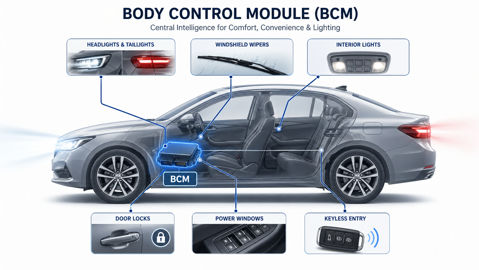
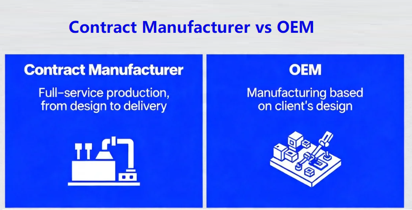
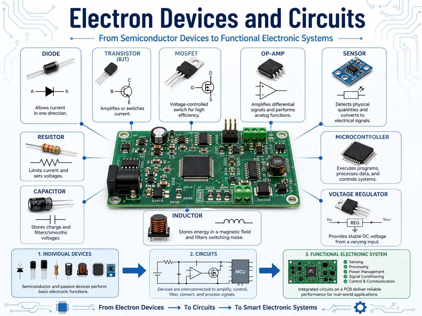
What Are Electron Devices and Circuits?
Electron devices and circuits are the foundation of electronic products. An electron device is a component that controls current, voltage, or signal behavior. A circuit is the connected network that allows these devices to perform a useful function, such as switching, amplification, filtering, rectification, sensing, timing, or power conversion.
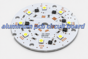
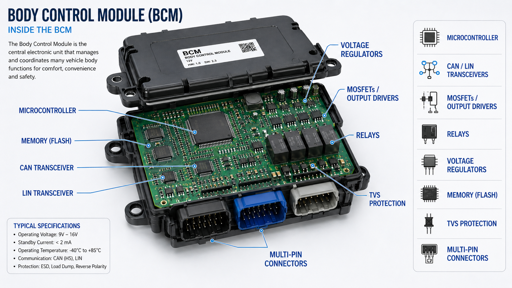
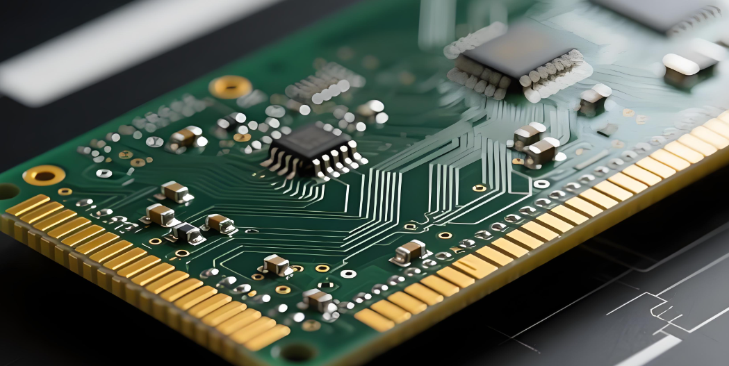
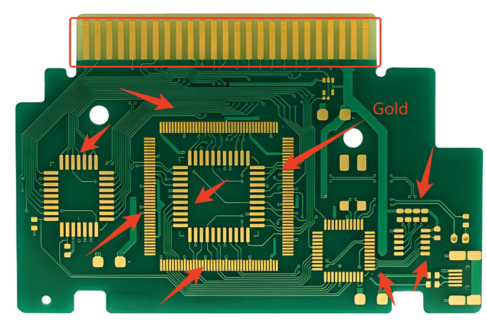
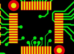
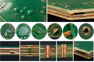
Common electron devices include diodes, transistors, MOSFETs, integrated circuits, sensors, voltage regulators, and operational amplifiers. These parts do not work alone in a finished product. They are connected through copper traces, vias, pads, and planes on a printed circuit board.
In simple terms, a device is the part. A circuit is the working system built with parts. A PCB is the physical platform that makes the circuit reliable, manufacturable, and suitable for real-world use.
Why Are Electron Devices and Circuits Important in Modern Electronics?
Electron devices and circuits are important because almost every electronic product depends on them to process signals, control power, and respond to the outside world. Without them, a PCB would only be a passive copper structure. The devices give the board intelligence, control, and function.
Modern electronics use circuits in many forms, a medical monitor uses sensor circuits and signal conditioning. An electric vehicle uses power control circuits and protection circuits. A telecom product uses RF circuits and high-speed digital paths. Industrial equipment uses control circuits, relay drivers, motor drivers, and power supply sections.
What Is the Difference Between Electronic Devices and Electronic Circuits?
Electronic devices are individual components. Electronic circuits are functional networks made by connecting those components. The difference is similar to the relationship between bricks and a building. A component may have a clear function, but the circuit decides how that function is used.
| Item | Meaning | Example | PCB Concern |
|---|---|---|---|
| Electronic device | A single component that controls or responds to electricity | Diode, MOSFET, IC, sensor | Footprint, polarity, package, rating |
| Electronic circuit | A connected group of devices and passive parts | Amplifier, filter, power supply | Routing, grounding, noise, heat |
| PCB layout | The physical copper and component arrangement | Traces, vias, planes, pads | Manufacturability and signal quality |
| PCBA | A finished assembled circuit board | PCB with components soldered | Testing, inspection, reliability |
| Final system | The board inside a working product | Medical device, IoT module, inverter | Compliance, durability, user safety |
A circuit may look correct on a schematic but still perform poorly on the actual PCB. Long current loops, weak grounding, wrong component placement, thin copper paths, or poor thermal design can change the behavior of the circuit. This is why circuit design and PCB layout should not be treated as separate jobs.
What Are the Main Types of Electron Devices?
The main types of electron devices include diodes, bipolar junction transistors, MOSFETs, IGBTs, operational amplifiers, sensors, voltage regulators, and integrated circuits. Each device has a specific role in controlling current, voltage, timing, power, or signal behavior. Below are the most common electronic components in the market and their basic functions:
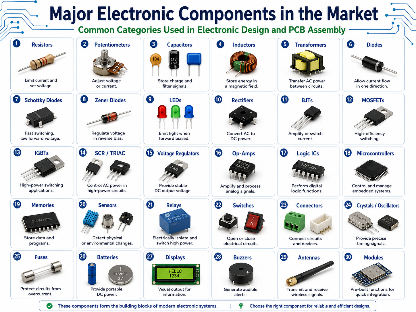
For PCB projects, the selected device package is as important as the device itself. A MOSFET in a small SOT-23 package cannot dissipate the same heat as a larger DPAK or PowerPAK package. A high-speed IC may require controlled impedance routing. A sensor may need clean analog grounding and physical isolation from heat sources.
How Do Diodes Work in Electronic Circuits?
Diodes mainly control current direction. They are often used to convert AC to DC, protect circuits from reverse polarity, clamp voltage spikes, and provide flyback protection for inductive loads such as relays, coils, and motors.
A standard silicon diode often has a forward voltage drop of about 0.6–0.8 V under typical operating conditions. A Schottky diode usually has a lower forward voltage, often around 0.2–0.5 V, making it useful in low-voltage and power-sensitive circuits.
| Diode Type | Typical Forward Voltage | Common Use | PCB Design Focus |
|---|---|---|---|
| Silicon diode | 0.6–0.8 V | Rectification, protection | Polarity, current rating |
| Schottky diode | 0.2–0.5 V | Low-loss power paths | Leakage current, heat |
| Zener diode | Depends on Zener voltage | Voltage clamp/reference | Power dissipation |
| TVS diode | Application-specific | ESD/surge protection | Place close to connector |
| LED | 1.8–3.3 V typical | Indication, lighting | Current limit and heat |
How Do Transistors and MOSFETs Control Current?
Transistors and MOSFETs control current by using a smaller signal to manage a larger load. A BJT is commonly driven by base current, while a MOSFET is driven by gate voltage. Both can switch loads, but MOSFETs are often preferred for efficient power switching.
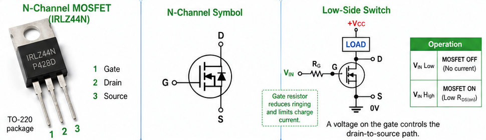
A BJT may be useful for small-signal amplification and low-current switching. A MOSFET is widely used in DC-DC converters, motor drivers, LED drivers, battery protection circuits, and power distribution boards. The choice depends on voltage, current, switching speed, drive voltage, heat, package size, and cost.
What Are the Most Common Electronic Circuit Types?
The most common electronic circuit types include rectifier circuits, amplifier circuits, filter circuits, oscillator circuits, switching circuits, voltage regulator circuits, sensor interface circuits, logic circuits, and power supply circuits. Each one solves a specific electrical task.
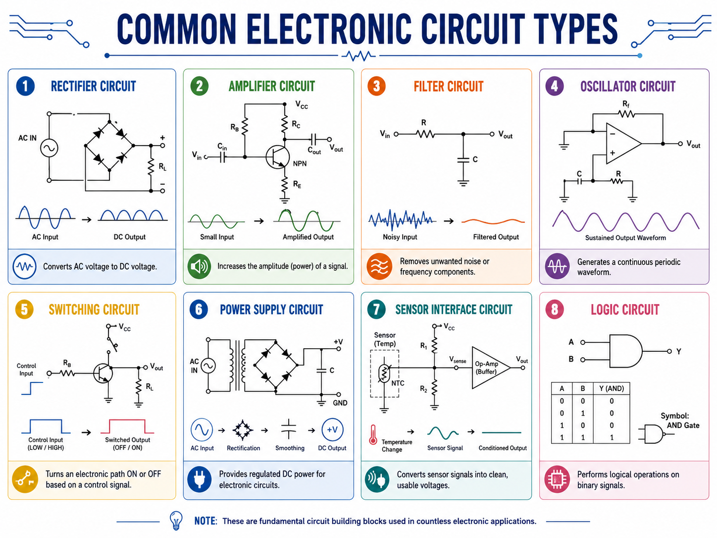
A practical PCB often contains several circuit types on the same board. For example, an industrial control board may include power input protection, DC-DC conversion, MCU logic, sensor input, relay output, and communication ports. The design challenge is to make these sections work together without noise, overheating, or assembly issues.
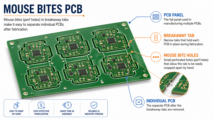
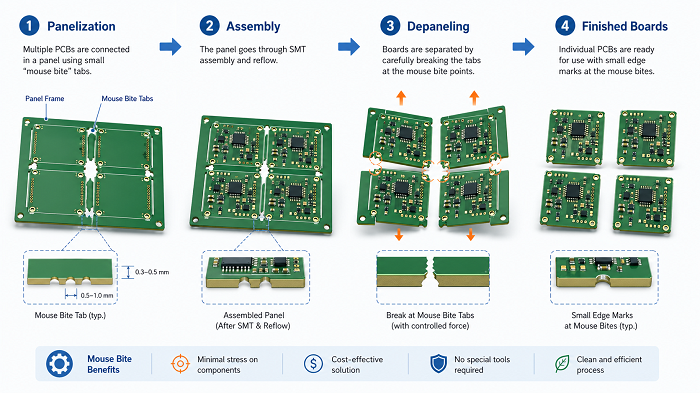
How Do Electron Devices and Circuits Become a PCB?
Electron devices and circuits become a PCB through a structured process: schematic design, BOM preparation, PCB layout, design review, Gerber output, fabrication, component sourcing, SMT assembly, inspection, testing, and final shipment. The schematic defines the electrical logic. The PCB layout turns that logic into a manufacturable board.
The process usually starts with circuit requirements, such as: What voltage does the board need? What current will it carry? What signals are sensitive? What connector, enclosure, and environmental requirements must be considered? These answers guide the schematic and layout.
A typical flow looks like this:
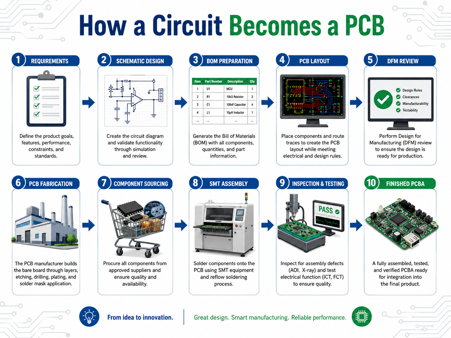
1. Define product function and electrical requirements.
2. Select suitable components and packages.
3. Build the schematic and check circuit behavior.
4. Create the PCB stack-up and layout rules.
5. Place components according to function, heat, and signal flow.
6. Route power, ground, analog, digital, and high-speed signals.
7. Add test points, markings, fiducials, and assembly details.
8. Run DRC, ERC, DFM, and DFT checks.
9. Fabricate the bare PCB.
10. Source components and prepare SMT programming.
11. Assemble the board through SMT, DIP, or mixed assembly.
12. Inspect and test the PCBA before delivery.
The earlier manufacturability is considered, the smoother the project becomes. A schematic can be electrically correct, but if the selected package is unavailable, the footprint is wrong, or the thermal path is weak, the final build may face delay or rework.
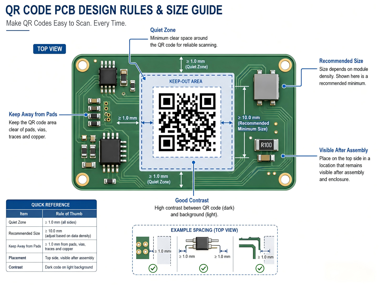
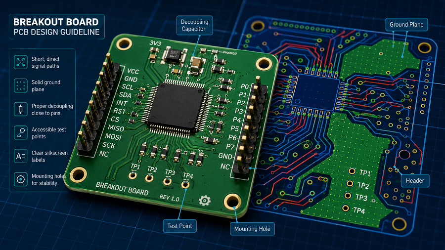
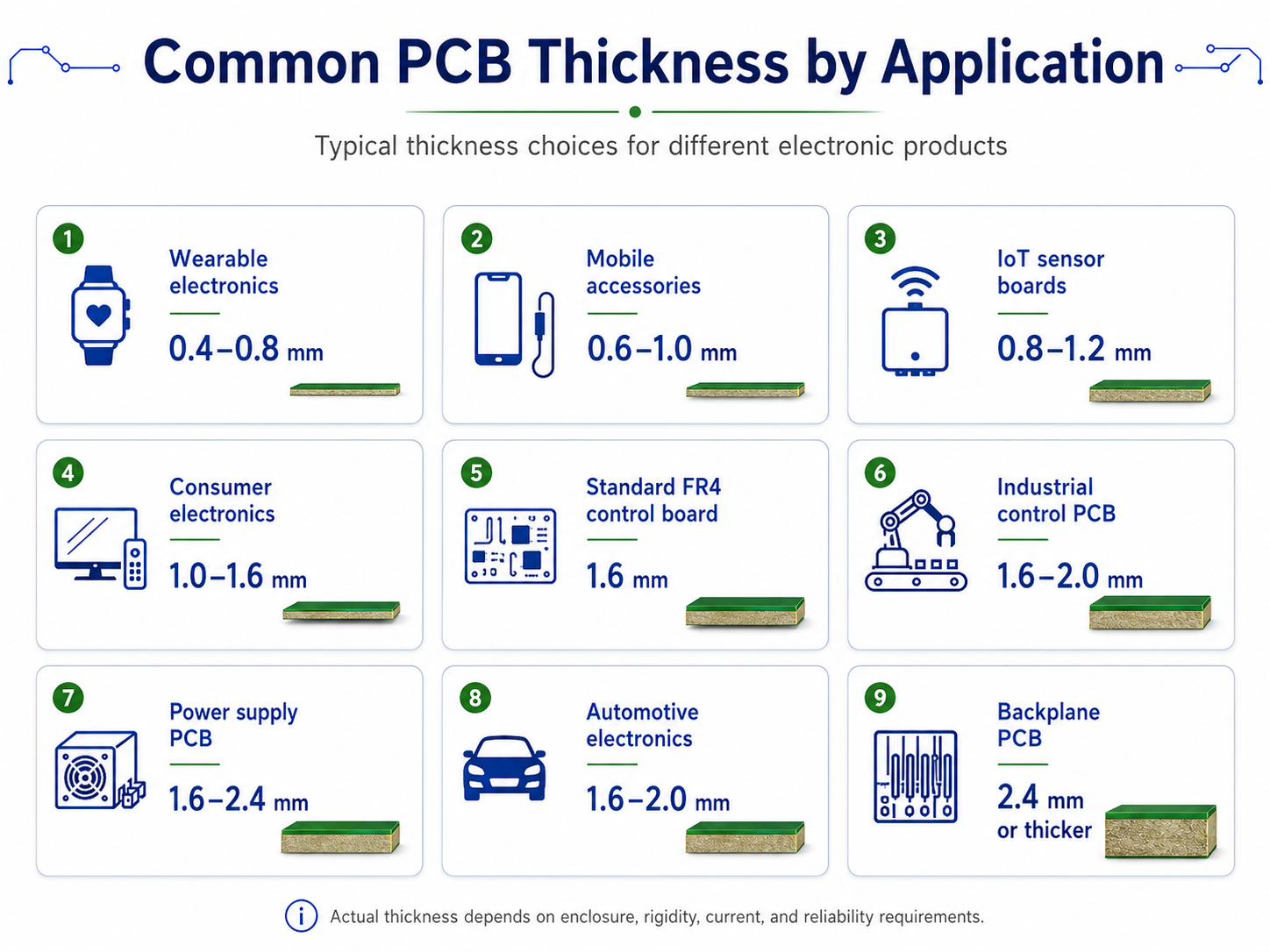
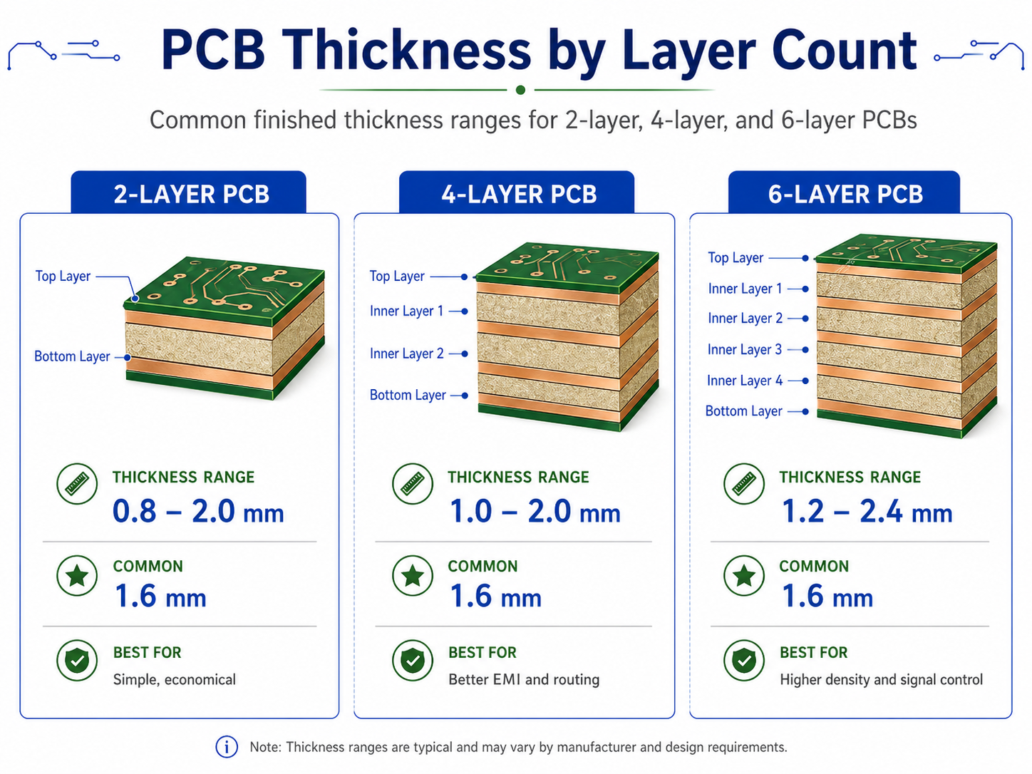
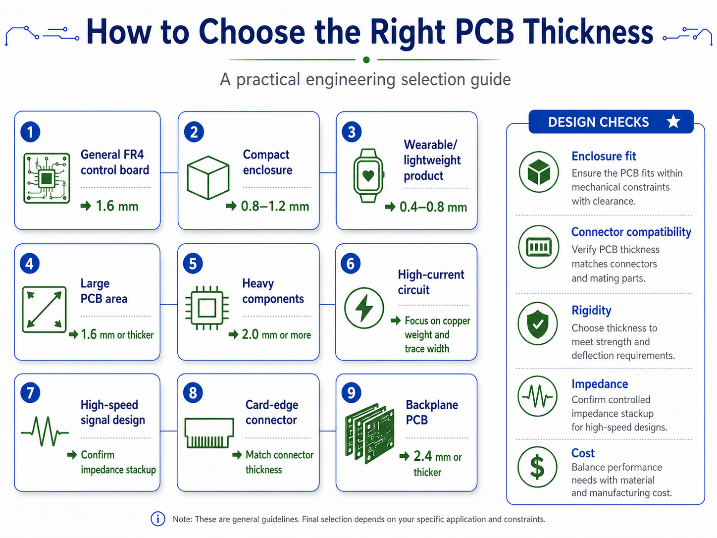
What PCB Design Rules Matter for Electronic Devices and Circuits?
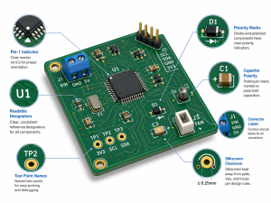
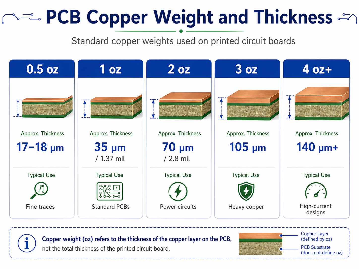
The PCB design rules that matter most include trace width, spacing, grounding, return path, decoupling capacitor placement, thermal relief, creepage, clearance, impedance control, component orientation, and test point access. These rules help the circuit perform as intended after manufacturing.
| Design Item | Why It Matters | Practical Rule of Thumb |
|---|---|---|
| Trace width | Controls current capacity and heating | Wider copper for power paths |
| Spacing | Reduces short risk and voltage breakdown | Increase spacing for higher voltage |
| Ground plane | Provides stable reference and return path | Use continuous ground where possible |
| Decoupling capacitor | Stabilizes IC power pins | Place close to power pins |
| Thermal via | Moves heat to other copper layers | Use near power IC pads |
| Test point | Supports inspection and troubleshooting | Add to power rails and signals |
| Component orientation | Reduces assembly mistakes | Keep polarity markings clear |
| Controlled impedance | Maintains high-speed signal quality | Define stack-up early |
One useful principle is to place parts according to current and signal flow. Power input should connect logically to protection, filtering, conversion, and load sections. Sensitive analog circuits should stay away from noisy switching nodes and high-speed signals should avoid unnecessary stubs and discontinuities.
What Causes Electron Devices and Circuits to Fail?
Electron devices and circuits usually fail because of overstress, poor layout, incorrect component selection, weak soldering, thermal buildup, electrical noise, or manufacturing defects. Many failures can be reduced through early design review and proper test planning.
Common causes include:
| Failure Cause | What Happens | How to Reduce the Risk |
|---|---|---|
| Overcurrent | Device or trace overheats | Use current rating, fuse, wider copper |
| Overvoltage | IC or diode damage | Add TVS, Zener, clamp, margin |
| ESD | Sudden device failure | Use ESD protection near connectors |
| Thermal stress | Drift, aging, solder fatigue | Add copper area, vias, airflow path |
| Wrong footprint | Assembly mismatch | Check datasheet and land pattern |
| Poor solder joint | Intermittent function | Use AOI, X-ray, proper stencil design |
| Noise coupling | Signal error or reset | Separate noisy and sensitive circuits |
| Weak test coverage | Hidden defects | Add ICT/flying probe/function test |
How Should Beginners Learn Electron Devices and Circuits?
Beginners should learn electron devices and circuits in a step-by-step order: basic electrical laws, passive components, diodes, transistors, MOSFETs, op-amps, power circuits, digital logic, PCB layout, and testing. This path makes the subject easier because each new topic builds on the previous one.
A good learning route starts with voltage, current, resistance, and power. Then it moves into resistors, capacitors, and inductors. After that, diodes and transistors become easier to understand. Once active devices are clear, amplifiers, filters, regulators, and switching circuits become more practical.
A beginner-friendly study path may look like this:
| Learning Stage | What to Learn | Practical Exercise |
|---|---|---|
| Stage 1 | Voltage, current, resistance, power | Calculate LED current resistor |
| Stage 2 | Resistors, capacitors, inductors | Build RC filter |
| Stage 3 | Diodes and rectifiers | Build bridge rectifier |
| Stage 4 | BJT and MOSFET switching | Drive LED, relay, or motor |
| Stage 5 | Op-amp circuits | Build non-inverting amplifier |
| Stage 6 | Power supply circuits | Test regulator output and ripple |
| Stage 7 | PCB layout basics | Convert schematic to PCB |
| Stage 8 | Testing and debugging | Measure voltage, current, waveform |
How Are Electron Devices and Circuits Used in Real PCB Applications?
Electron devices and circuits are used in almost every PCB application, including medical electronics, automotive systems, telecom equipment, industrial control, robotics, power electronics, smart sensors, LED lighting, consumer devices, and IoT products. Here we listing some applications of electron devices and their typical circuit needs:
| Application | Typical Circuit Needs |
|---|---|
| Medical electronics | Sensor input, signal conditioning, power control |
| Industrial control | Relay output, PLC interface, motor control |
| Automotive electronics | Power switching, communication, protection |
| Telecom equipment | RF, high-speed digital, power supply |
| IoT devices | MCU, wireless module, battery management |
| LED lighting | Constant-current driver, thermal path |
| Robotics | Motor driver, sensor fusion, control logic |
How Can PCB Layout Improve Circuit Performance?
PCB layout can improve circuit performance by reducing noise, controlling heat, shortening current loops, protecting sensitive signals, and making the board easier to assemble and test. Layout is not only about connecting pins, it directly affects electrical behavior.
Several layout habits are helpful:
- Place decoupling capacitors close to IC power pins.
- Keep high-current paths short and wide.
- Avoid routing sensitive analog signals near switching nodes.
- Use a continuous ground plane where possible.
- Place protection devices close to external connectors.
- Add enough test points for production and troubleshooting.
- Review footprints before releasing Gerber files.
- Separate hot components from temperature-sensitive parts.
A clean layout can make a modest circuit perform very well. A poor layout can make a good schematic unstable.
How Can EBest Support PCB Projects for Electron Devices and Circuits?
EBest supports PCB projects by helping customers move from schematic and BOM to PCB fabrication, component sourcing, PCBA assembly, testing, and delivery. This is useful for projects that involve power circuits, sensor circuits, control boards, communication modules, medical electronics, industrial electronics, automotive electronics, and telecom hardware.
EBest Circuit provides:
- PCB fabrication for prototypes and production
- PCBA assembly for SMT, DIP, and mixed-technology boards
- Component sourcing and BOM optimization
- DFM review before manufacturing
- AOI, X-ray, ICT, flying probe, and functional testing options
- Engineering communication for complex PCB and PCBA projects
- Support for industrial, medical, automotive, telecom, IoT, and power electronics applications
A circuit becomes valuable only when it can be built reliably. By combining PCB manufacturing, assembly, sourcing, and testing, EBest helps customers reduce communication gaps and move faster from design files to finished boards.
For project review, customers can send schematic, BOM, Gerber files, or assembly drawings to sales@bestpcbs.com.
FAQs About Electron Devices and Circuits
1. What are electron devices and circuits?
Electron devices and circuits are the components and connections that allow electronic systems to control current, voltage, signals, and power. Devices include diodes, transistors, MOSFETs, ICs, sensors, and op-amps. Circuits connect these parts to perform functions such as switching, amplification, filtering, protection, sensing, and power conversion.
2. What is the difference between electrical circuits and electronic circuits?
An electron device is an individual component (like a transistor or diode) that controls the flow of electrons to perform a specific function. An electronic circuit is a complete path or network of these devices connected together with passive components (resistors, capacitors) to process signals or manage power.
3. Why is silicon the most commonly used material in electron devices?
Silicon is preferred because it is abundant, relatively inexpensive, and has excellent thermal stability. Most importantly, it naturally forms a high-quality silicon dioxide layer, which is essential for manufacturing MOSFETs (Metal-Oxide-Semiconductor Field-Effect Transistors), the building blocks of modern chips.
4. How does a P-N junction diode work?
A P-N junction diode is formed by joining p-type (positive) and n-type (negative) semiconductor materials. It acts as a one-way valve for electricity: in “forward bias,” it allows current to flow easily, whereas in “reverse bias,” it blocks current by creating a depletion region that prevents electrons from crossing.
5. What is the difference between analog and digital circuits?
Analog circuits process continuous signals that vary in voltage or current (like sound waves). Digital circuits process discrete signals, representing data as “high” or “low” voltages (1s and 0s). While analog is used for real-world sensing, digital is favored for processing and data storage due to its resistance to noise.