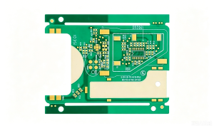
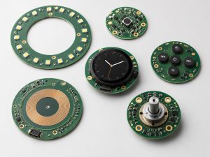
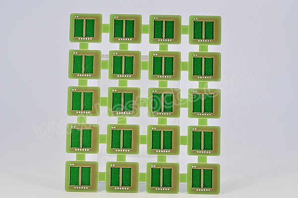
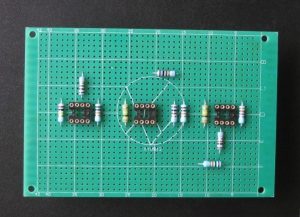
A 94V0 circuit board is commonly used in electronic products that require flame-retardant PCB materials, stable insulation, reliable assembly, and long-term safety. Buyers often search for this term when they need custom PCBs for power supplies, LED lighting, chargers, routers, smart devices, industrial controllers, consumer electronics, or OEM electronic products.
Best Technology provides custom 94V0 PCB manufacturing and PCBA services from prototype to batch production. Our team supports DFM review, BOM optimization, PCB fabrication, component sourcing, SMT assembly, DIP assembly, functional testing, and production traceability. If you need a quote, send your Gerber files, BOM, quantity, and testing requirements to sales@bestpcbs.com.
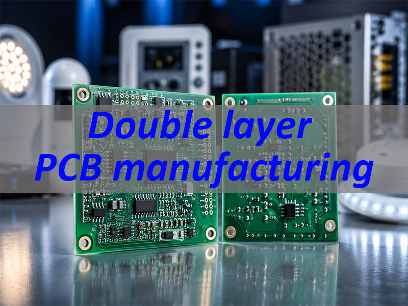
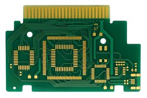
What Is a 94V0 Circuit Board?
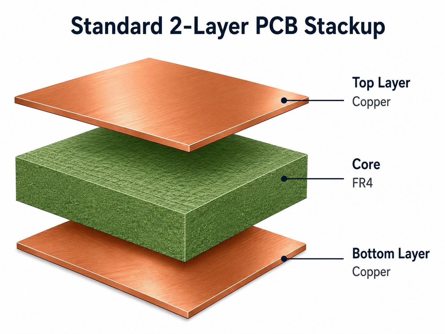
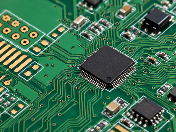
A 94V0 circuit board is a printed circuit board made with a material system that meets a flame-retardant classification commonly known as 94V0 or UL 94V-0. The mark may appear on the PCB surface, solder mask, silkscreen, material label, or technical document.
It is important to understand one point first: 94V0 is not a circuit function. A board marked 94V0 can be a power supply board, LED PCB, charger PCB, router PCB, appliance control board, industrial control PCB, or complete PCBA.
It is also not the name of one fixed PCB material. Many FR4 laminates can meet 94V0 requirements. Some CEM-1 boards, aluminum PCBs, high Tg FR4 boards, and other material systems may also be selected according to the product design.
In purchasing language, “94V0 circuit board” usually means the customer needs a PCB with flame-retardant material support, stable electrical performance, and reliable manufacturing control. For OEM projects, this requirement should be checked together with board thickness, copper thickness, solder mask, surface finish, assembly method, and test plan.
What Does 94V0 Mean on a Printed Circuit Board?
94V0 usually refers to a flame-retardant rating. In PCB manufacturing, it is commonly connected with the UL 94V-0 flammability classification. The “V” refers to vertical burning, while “0” indicates a high flame-retardant level in the vertical burning category.
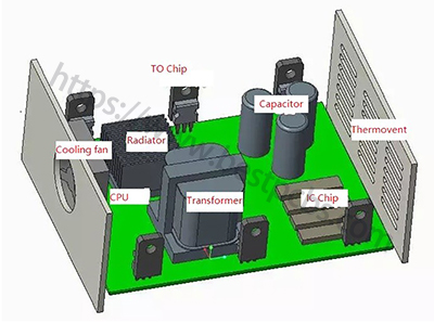
This rating is important because many electronic products work with heat, current, enclosed housing, and continuous operation. Power supplies, chargers, lighting modules, appliance boards, and industrial controllers all need reliable insulation and safer material behavior.
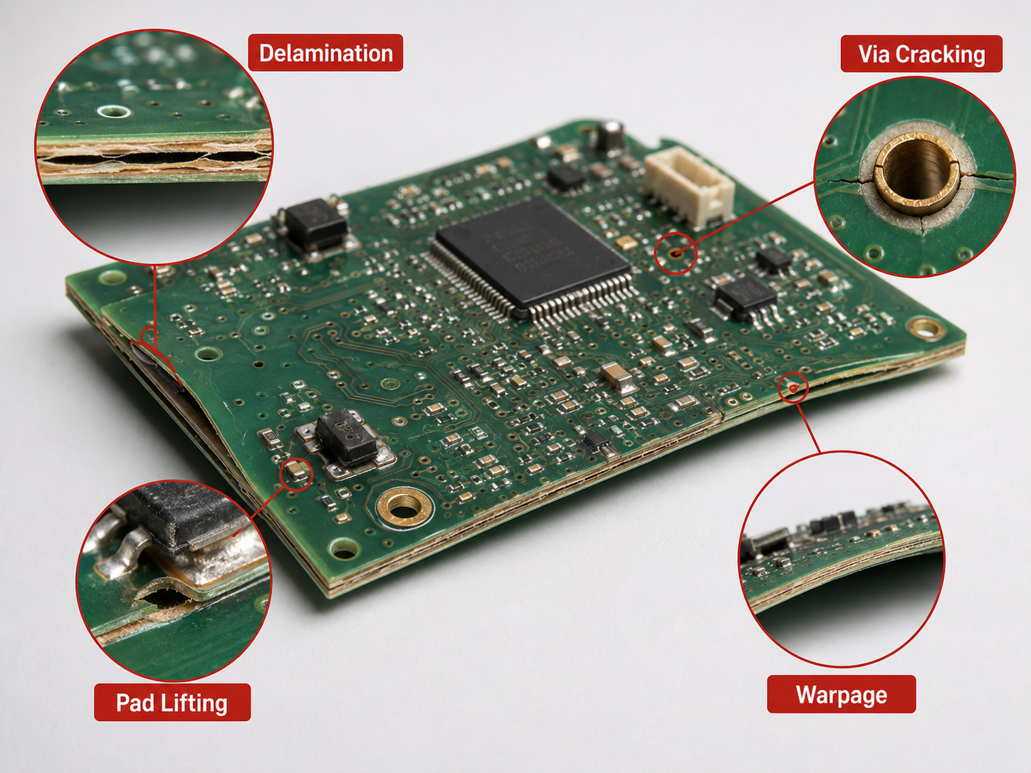
However, 94V0 is only one part of PCB quality. A professional PCB project should also check:
- Material type
- Copper thickness
- Board thickness
- Creepage and clearance
- Hole quality
- Plating quality
- Solder mask quality
- Surface finish
- Assembly process
- Electrical test
- Functional test
A 94V0 mark tells you something about flame-retardant performance. It does not fully define the circuit board’s electrical, thermal, mechanical, or assembly reliability.
Who Needs Custom 94V0 Circuit Board Manufacturing?
Custom 94V0 circuit board manufacturing is useful for customers who need reliable PCBs or PCB assemblies for electronic products with safety, performance, and production requirements.
This type of service is especially suitable for:
- OEM electronics brands
- Power supply manufacturers
- LED lighting companies
- Industrial control equipment manufacturers
- Charger and adapter suppliers
- Consumer electronics companies
- Smart home device manufacturers
- Engineering teams needing prototype-to-production support
If you are developing a new electronic product, you may need a supplier that can do more than fabricate bare boards. You may need engineering review, component sourcing, PCB assembly, testing, and batch production support.
For example, a power supply manufacturer may care about creepage, clearance, copper thickness, heat rise, and functional testing. An LED lighting company may focus more on thermal management, solder mask quality, LED polarity, and aging tests. An industrial control company may care about long-term reliability, traceability, and repeat production stability.
This is why choosing the right 94V0 circuit board manufacturer matters. The supplier should understand both PCB fabrication and real product application.
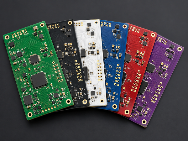
94V0 Circuit Board Manufacturing Capabilities at Best Technology
Best Technology supports custom PCB and PCBA projects for different electronic applications.
| Capability | Support |
|---|---|
| Materials | FR4, CEM-1, aluminum |
| Tg Options | Standard, high Tg |
| Layers | 1–32 layers |
| Copper | 0.5–20 oz |
| Min Hole | 0.15 mm |
| Laser Via | 0.10 mm |
| Line/Space | 3/3 mil |
| Thickness | 0.15–8.0 mm |
| Finish | OSP, HASL, ENIG |
| Assembly | SMT, DIP |
| Testing | AOI, X-ray, function |
| Orders | Sample to volume |
These capabilities allow Best Technology to support both simple and advanced 94V0 circuit board projects. For standard electronic products, FR4 or CEM-1 may be suitable. For higher heat or power applications, aluminum PCB, high Tg FR4, or heavier copper may be considered.
For PCBA projects, Best Technology provides electronic contract manufacturing service, including PCB fabrication, component sourcing, PCB SMT assembly, DIP assembly, inspection, testing, and packaging. This helps customers reduce supplier coordination and improve project efficiency.
Is 94V0 a PCB Material or a Flame-Retardant Rating?
94V0 should be understood as a flame-retardant rating reference, not a material name.
Many buyers search for “94V0 PCB material” because they see the mark on an existing board. In most cases, they actually need to confirm which material can meet the required flame-retardant performance and product conditions.
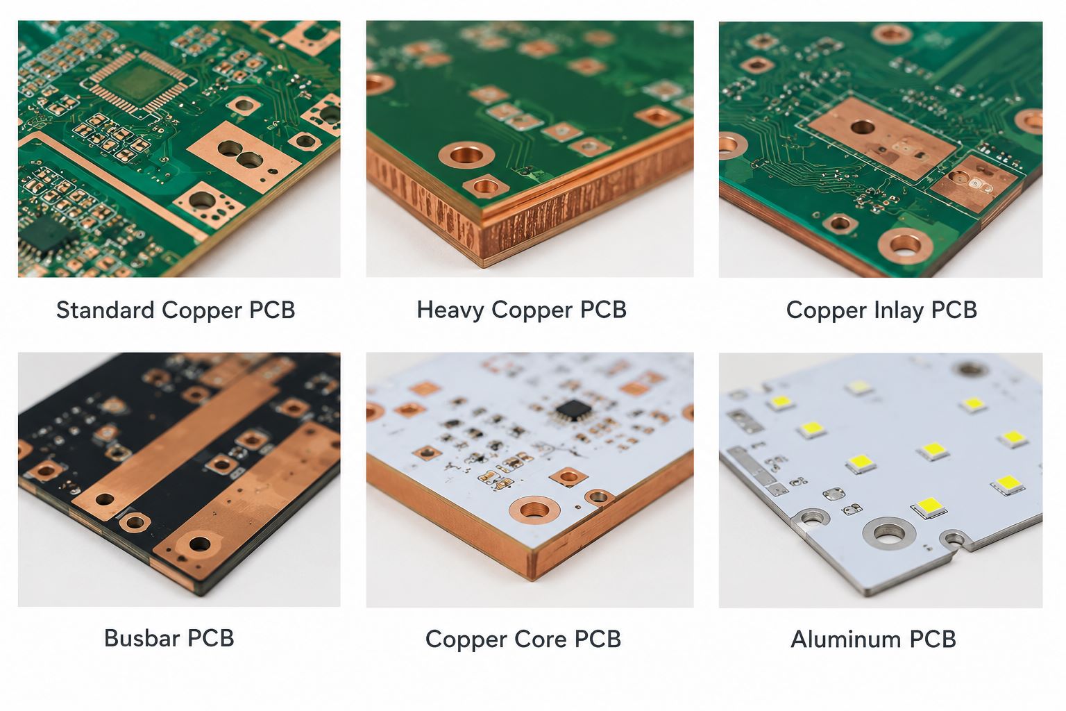
Common material choices include:
| Material | Best For |
|---|---|
| FR4 | General electronics |
| High Tg FR4 | Higher heat |
| CEM-1 | Cost-sensitive boards |
| Aluminum PCB | Thermal designs |
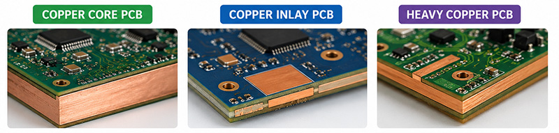
| Heavy copper PCB | Higher current |
| HDI PCB | Compact devices |
FR4 is the most common choice for many 94V0 circuit boards. It offers good insulation, mechanical strength, process stability, and cost balance. It is suitable for single-sided, double-sided, and multi-layer PCBs.
CEM-1 is often used in simpler and more cost-sensitive products. It is common in some lighting products, household appliances, and simple consumer electronics.
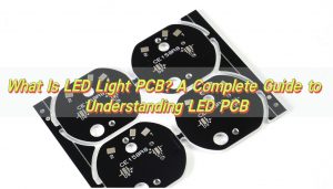
Aluminum PCB is selected when heat dissipation is important. LED lighting boards, power modules, and other heat-generating circuits may benefit from a metal core structure.
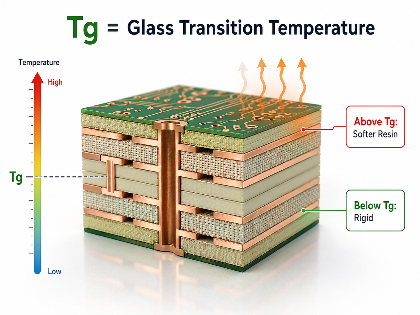
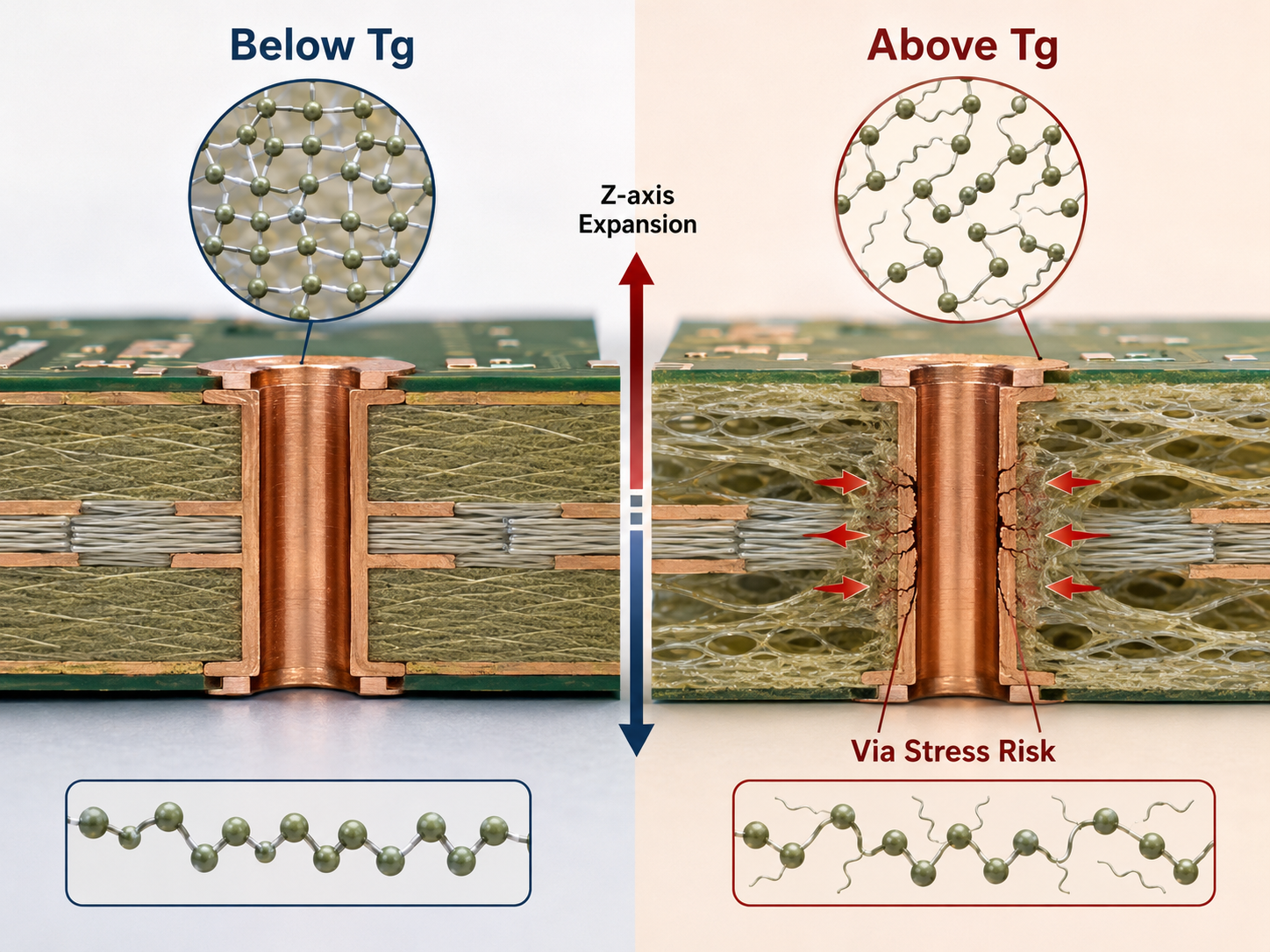
High Tg FR4 is useful when the board needs better thermal stability during assembly or operation. It is often used in industrial, automotive, medical, and higher-reliability electronics.
The right material should be selected according to the working temperature, current load, product structure, reliability target, and budget.
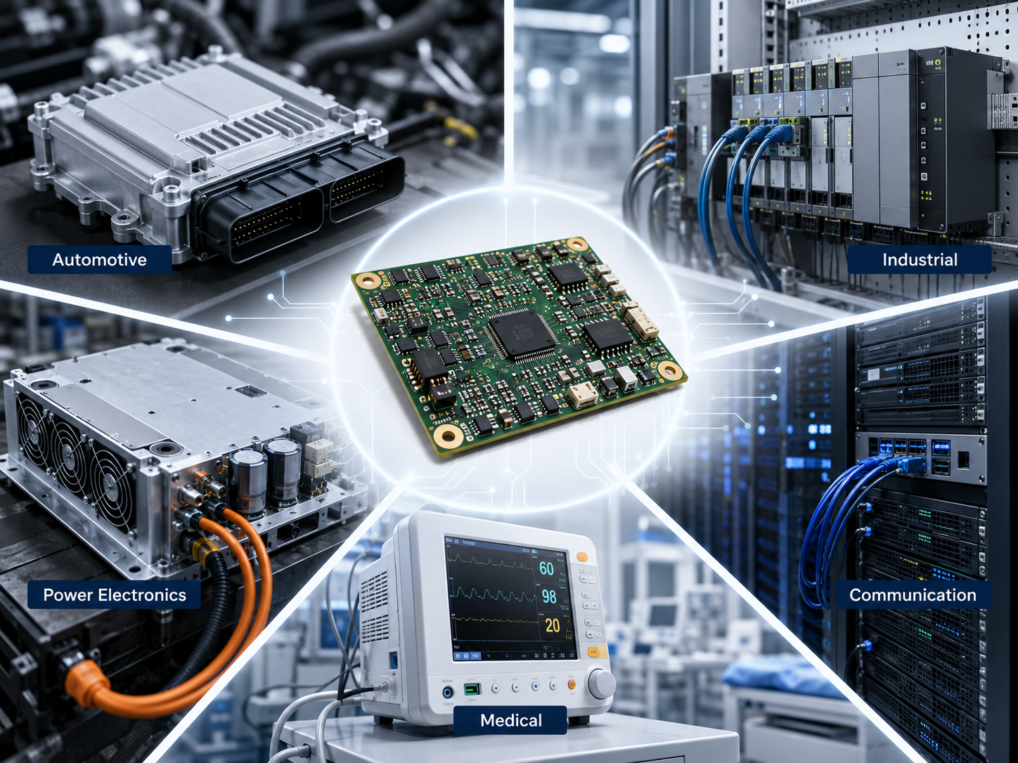
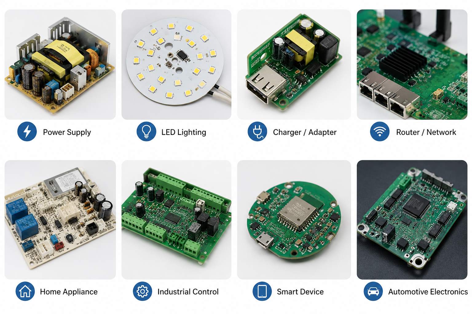
What Are Common Applications of 94V0 Circuit Boards?
94V0 circuit boards are used in many electronic products because flame-retardant material support is valuable in both consumer and industrial applications.
| Application | Key Concern |
|---|---|
| Power supply | Safety spacing |
| LED lighting | Heat control |
| Charger | Compact layout |
| Router | Signal stability |
| Appliance | Cost balance |
| Industrial control | Reliability |
| Smart device | Stable assembly |
| Automotive electronics | Process control |
In power supply products, the PCB must handle voltage, current, insulation distance, and heat rise. The design should pay attention to copper thickness, creepage, clearance, and solder joint reliability.
In LED lighting products, thermal management is often the main concern. Low-power products may use FR4 or CEM-1, while higher-power lighting usually requires aluminum PCB or other better thermal solutions.
In routers and communication devices, stack-up design, grounding, signal routing, and material consistency become more important. A 94V0 label alone cannot define signal performance.
In industrial control systems, the board may work inside machines, cabinets, automation equipment, or power control devices. These products need reliable assembly, testing, traceability, and stable repeat production.
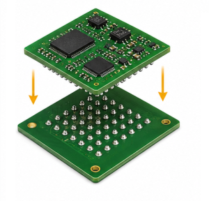
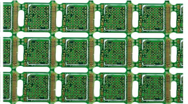
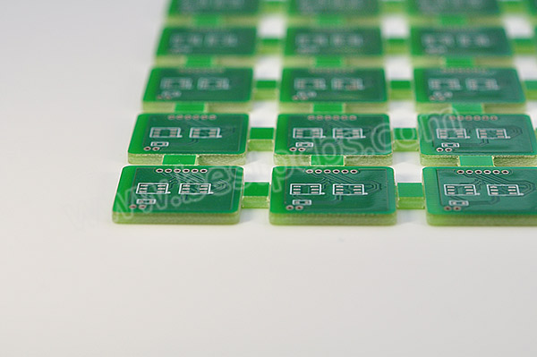
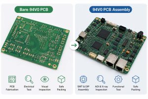
Bare 94V0 PCB vs 94V0 PCB Assembly: Which Service Do You Need?
When sourcing a 94V0 circuit board, the first question is whether you need a bare PCB or a complete PCB assembly.
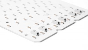
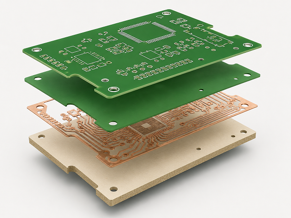
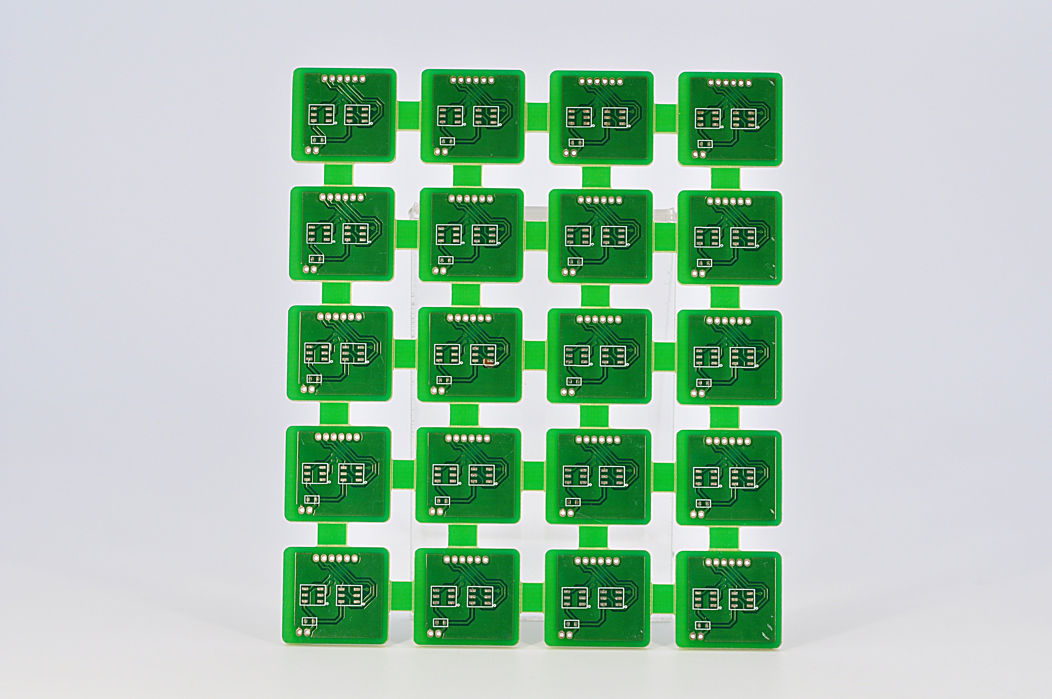
A bare PCB is the fabricated board without components. It includes the substrate, copper traces, solder mask, silkscreen, holes, plating, surface finish, and board outline.
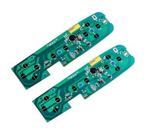
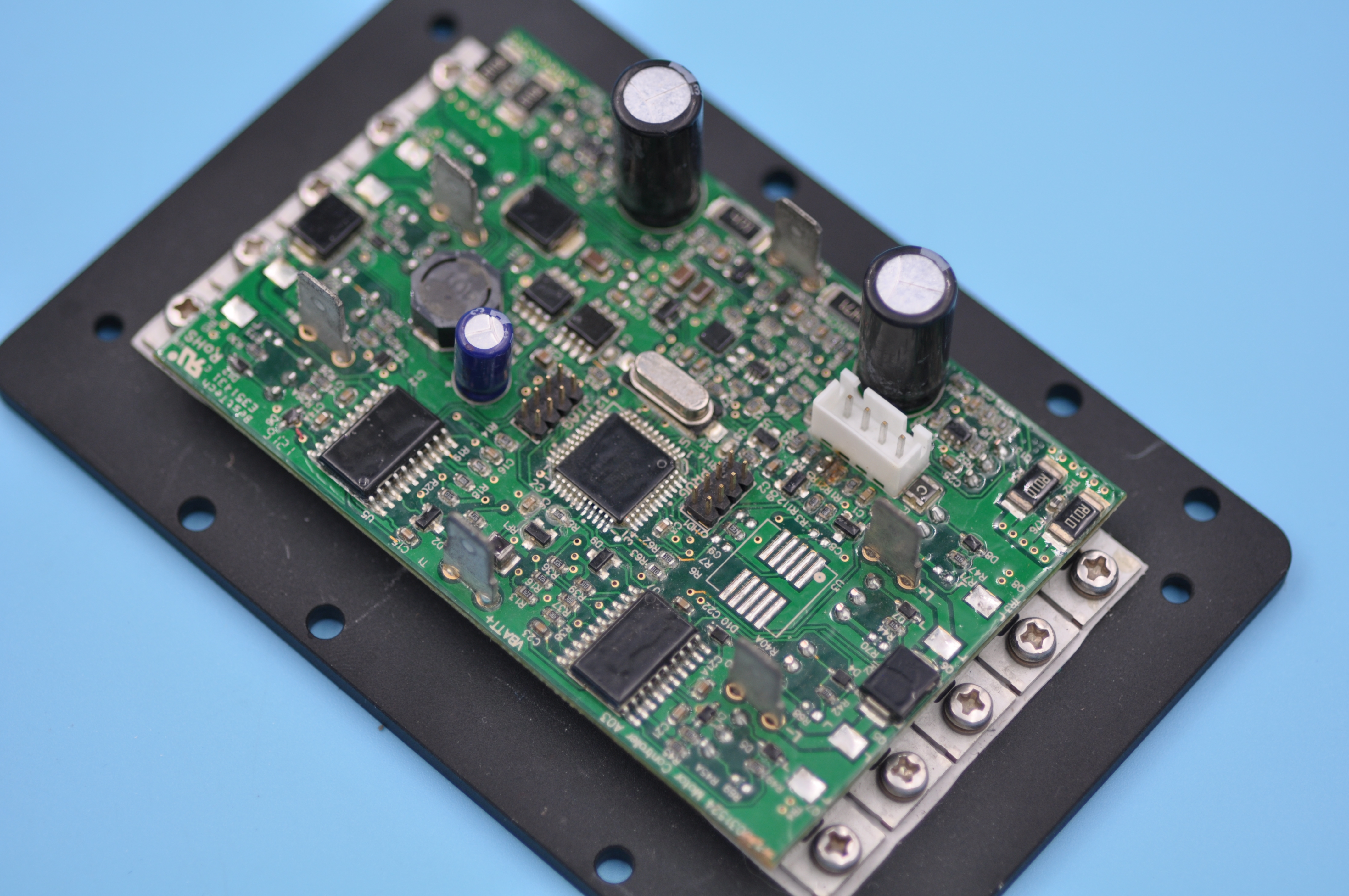
A PCBA is a finished board with components mounted and soldered. It may include resistors, capacitors, ICs, connectors, LEDs, transformers, switches, sensors, and other electronic parts.
| Service | Includes |
|---|---|
| Bare PCB | Board only |
| PCBA | Board + parts |
| Turnkey PCBA | PCB + sourcing |
| Testing | Electrical or function |
| Box build | Final assembly |
If you already have your own assembly line, bare PCB fabrication may be enough. If you need a ready-to-test or ready-to-install electronic board, PCBA service is usually a better choice.
Best Technology supports both bare PCB manufacturing and turnkey PCBA. This gives OEM customers more flexibility during prototype development, trial production, and mass production.

How Best Technology Manufactures Custom 94V0 Circuit Boards
A custom 94V0 circuit board project starts with file review. Before production, Best Technology checks whether the design is suitable for the selected material, copper thickness, hole structure, line width, spacing, solder mask, and surface finish.
The general process includes:
| Step | Purpose |
|---|---|
| File review | Check risks |
| Material choice | Match use |
| PCB fabrication | Build board |
| Surface finish | Solderability |
| Electrical test | Opens/shorts |
| Assembly | Mount parts |
| Inspection | Find defects |
| Functional test | Confirm use |
| Packing | Protect boards |
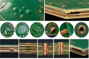
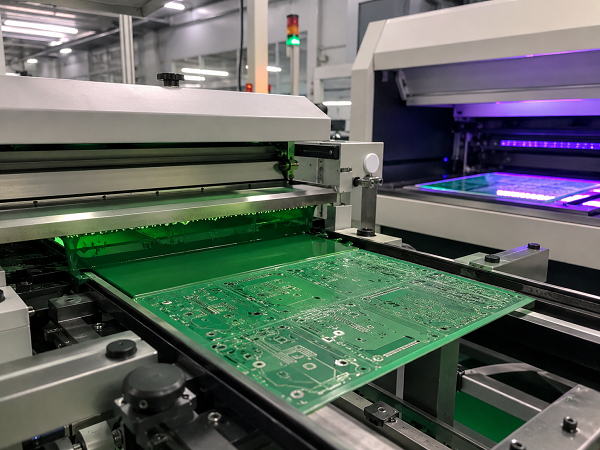
For bare PCB production, the process may include material preparation, imaging, etching, lamination, drilling, copper plating, solder mask, silkscreen, surface finish, profiling, electrical testing, and final inspection.
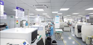
For PCBA production, the process continues with solder paste printing, component placement, reflow soldering, AOI inspection, DIP assembly, selective soldering or wave soldering, cleaning, functional testing, and final packaging.
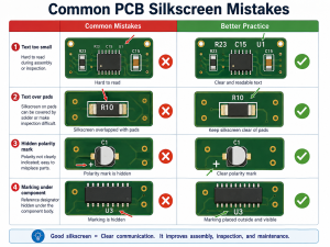
Best Technology also provides DFM review before production. Our engineers can check risks such as narrow spacing, insufficient annular ring, unclear polarity, missing test points, unsuitable pad design, poor copper balance, and difficult assembly areas.
This is useful because many PCBA problems do not start on the SMT line. They often start from design details that were not checked before production.
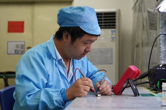
How Do We Verify Quality in 94V0 PCB and PCBA Production?
Quality control should begin before production. A reliable PCB supplier should check design risks, material selection, process feasibility, assembly quality, and final function.
Best Technology uses engineering review, process inspection, production tracking, and testing to support stable quality.
| Quality Step | Check Point |
|---|---|
| DFM | Design risk |
| Material check | PCB spec |
| Drilling check | Hole accuracy |
| Plating check | Copper quality |
| Solder mask | Opening quality |
| Electrical test | Open/short |
| AOI | SMT defects |
| X-ray | Hidden joints |
| Functional test | Product function |
| Traceability | Batch tracking |
For PCB fabrication, electrical testing helps detect open and short circuits. Dimensional inspection checks whether the outline, holes, slots, and tolerances meet requirements.
For PCBA, AOI checks missing parts, wrong parts, polarity issues, tombstoning, solder bridges, and placement defects. X-ray can be used for BGA, QFN, and hidden solder joints when required.
Functional testing is important for OEM electronic products. A board should not only look correct. It should power on, communicate, switch, sense, light, charge, or control according to the product design.
Best Technology’s digital workshop supports fast tracking of materials, product batches, production cycles, and production progress. This helps improve delivery visibility and quality traceability.
What Files Should You Send for a 94V0 Circuit Board Quote?
To receive an accurate quotation, buyers should send complete project files. This helps reduce repeated communication and allows the engineering team to check cost, process, risk, and delivery more accurately.
For bare PCB quotation, please send:
- Gerber files
- Drill files
- Board thickness
- Copper thickness
- Material requirement
- Surface finish
- Solder mask color
- Quantity
- Delivery requirement
For PCBA quotation, please also send:
- BOM
- Pick-and-place file
- Assembly drawing
- Testing method
- Programming file
- Packaging requirement
- Special inspection notes
Best Technology can provide DFM pre-check support and BOM optimization suggestions when needed. Our experienced PCB and PCBA engineers can review manufacturability, component availability, process fit, and possible production risks.
This is especially helpful for engineering teams developing new products. Early review can improve layout reliability, assembly yield, and production readiness. For quotation, pls feel free to send your files to sales@bestpcbs.com.
Why Choose Best Technology for 94V0 Circuit Board Manufacturing?
Best Technology provides engineering-driven PCB and PCBA services for customers who need stable manufacturing support, technical response, and reliable delivery.
Our advantages include:
| Advantage | Value |
|---|---|
| 20-year experience | Strong know-how |
| PCB + PCBA factory | One-stop control |
| DFM support | Lower risk |
| BOM optimization | Better sourcing |
| 1000+ partners | Supply chain |
| 1800+ customers | Proven service |
| 10,000+ engineers | Engineering focus |
| Digital workshop | Fast traceability |
| Fast PCBA delivery | Project speed |
| Certifications | Quality trust |
Best Technology supports the full process from PCB fabrication to component sourcing, PCBA assembly, testing, and delivery. This helps customers reduce communication cost and improve project execution.
Our engineering team provides DFM analysis and process adaptation suggestions. This is valuable for customers who need more than a standard PCB quote. Many OEM projects require material advice, layout risk review, component availability checks, and testing planning before production.
Best Technology supports sample and small-batch orders, helping engineers verify designs and prepare for mass production. For suitable projects, PCBA delivery can be as fast as 1.5 weeks, depending on PCB complexity, component availability, testing requirements, and order quantity.
We also hold quality certifications including ISO9001, ISO13485, IATF16949, and AS9100D. These systems support projects in industrial, medical, automotive, aerospace, and other quality-sensitive markets.
How to Choose the Right 94V0 Circuit Board Manufacturer
Choosing a 94V0 circuit board manufacturer should not be based only on price. A low quotation may look attractive at first, but poor material selection, weak DFM review, unstable component sourcing, or incomplete testing can create higher cost later.
A reliable manufacturer should be able to answer these questions clearly:
- What material fits this product?
- Is FR4 enough?
- Is high Tg needed?
- Does the board need heavy copper?
- Are creepage and clearance safe?
- Is the design assembly-friendly?
- Are the components available?
- What testing is recommended?
- Can the supplier support repeat orders?
The best supplier should help identify risks before production. This is where engineering service becomes valuable. A good DFM review can turn manufacturing experience into practical suggestions before boards enter fabrication or assembly.
Best Technology works with engineers, buyers, and OEM teams to provide this type of support. Our goal is not only to produce circuit boards, but also to help customers build reliable electronic products with better manufacturing confidence.
FAQs about 94V0 Circuit Board
Q1: What does 94V0 mean on a circuit board?
94V0 usually refers to a flame-retardant rating related to PCB material performance. It is often connected with UL 94V-0 flammability classification.
Q2: Is 94V0 a PCB material?
No. 94V0 is not a material name. It is a flame-retardant rating reference. FR4, CEM-1, aluminum PCB material systems, and other substrates may be selected according to the project.
Q3: Is every FR4 PCB a 94V0 circuit board?
Not always. Many FR4 materials meet 94V0 requirements, but buyers should confirm the actual material datasheet and supplier documentation.
Q4: Can Best Technology manufacture custom 94V0 circuit boards?
Yes. Best Technology supports custom PCB manufacturing and PCB assembly for OEM projects based on Gerber files, BOM, and technical requirements.
Q5: Can you provide both bare PCB and PCBA?
Yes. We support bare PCB fabrication, component sourcing, SMT assembly, DIP assembly, testing, and turnkey PCBA service.
Q6: What applications use 94V0 circuit boards?
Common applications include power supplies, LED lighting, chargers, routers, industrial controllers, smart devices, consumer electronics, and automotive electronics.
Q7: What affects the price of a 94V0 circuit board?
Main factors include material, board size, layer count, copper thickness, surface finish, hole size, line width, assembly complexity, testing, quantity, and lead time.
Q8: What files are needed for quotation?
For PCB quotation, send Gerber files, board specifications, quantity, and delivery requirements. For PCBA quotation, also send BOM, pick-and-place file, assembly drawing, and testing requirements.
Q9: Can you help check my design before production?
Yes. Best Technology can provide DFM review, process suggestions, and BOM optimization support to help reduce production risks.
Q10: How fast can a 94V0 PCB assembly project be delivered?
Fast delivery depends on design complexity, PCB process, component availability, testing needs, and quantity. For suitable projects, PCBA delivery can be as fast as 1.5 weeks.
In conclusion, a 94V0 circuit board is more than a PCB with a flame-retardant mark. For OEM electronic products, it should be supported by proper material selection, DFM review, stable PCB fabrication, reliable assembly, functional testing, and production traceability.
If you are sourcing a custom 94V0 PCB or PCBA, Best Technology can support your project from prototype to batch production. Send your Gerber files, BOM, quantity, and testing requirements to sales@bestpcbs.com. Our engineering team will review your project and provide a suitable 94V0 circuit board manufacturing and assembly solution.