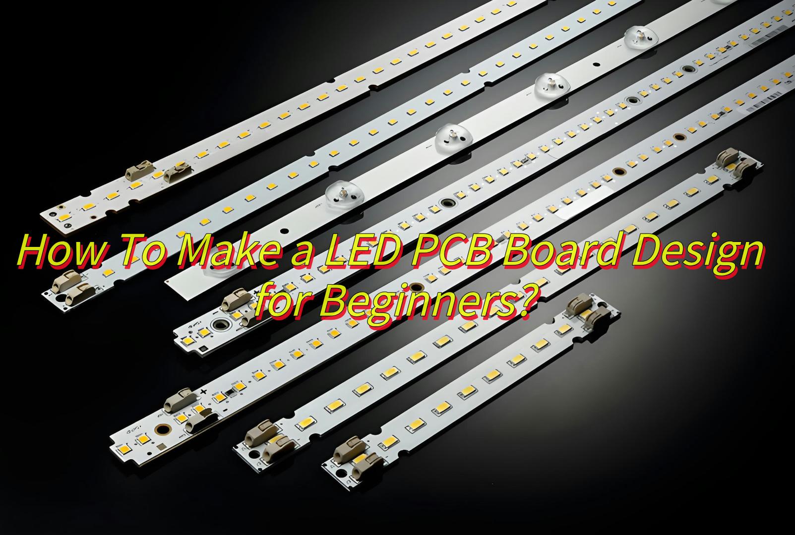
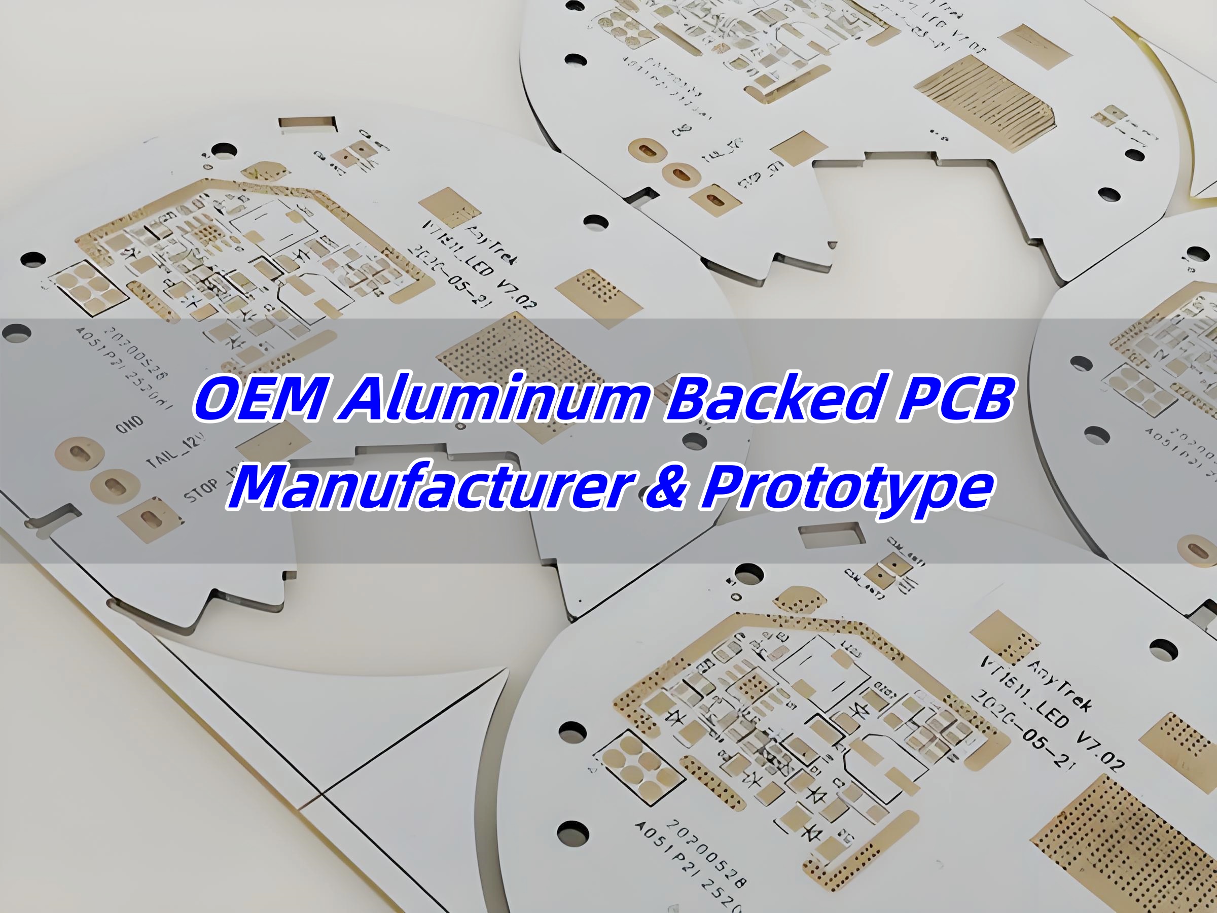
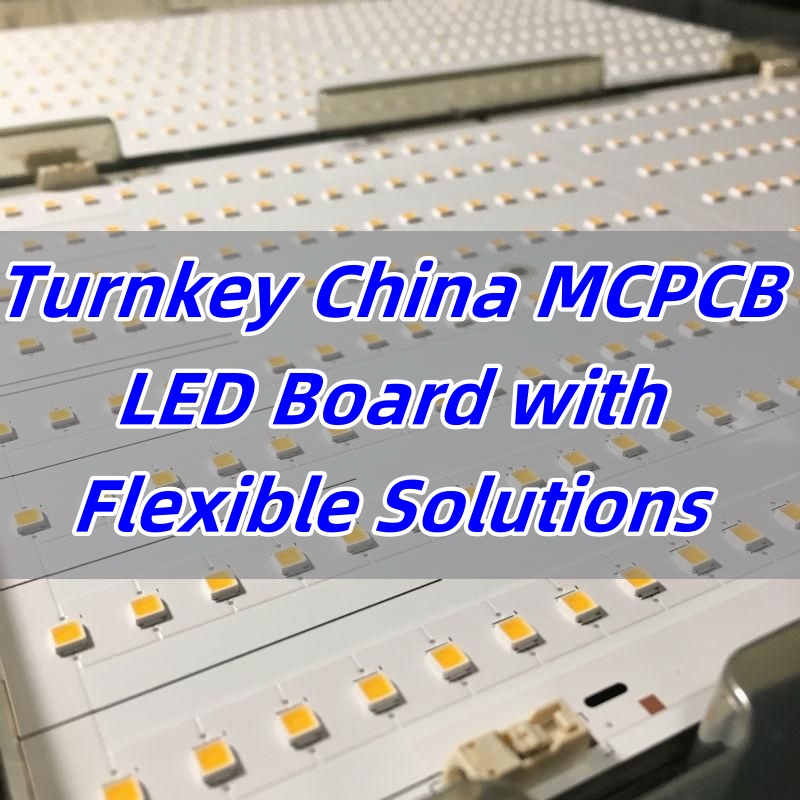
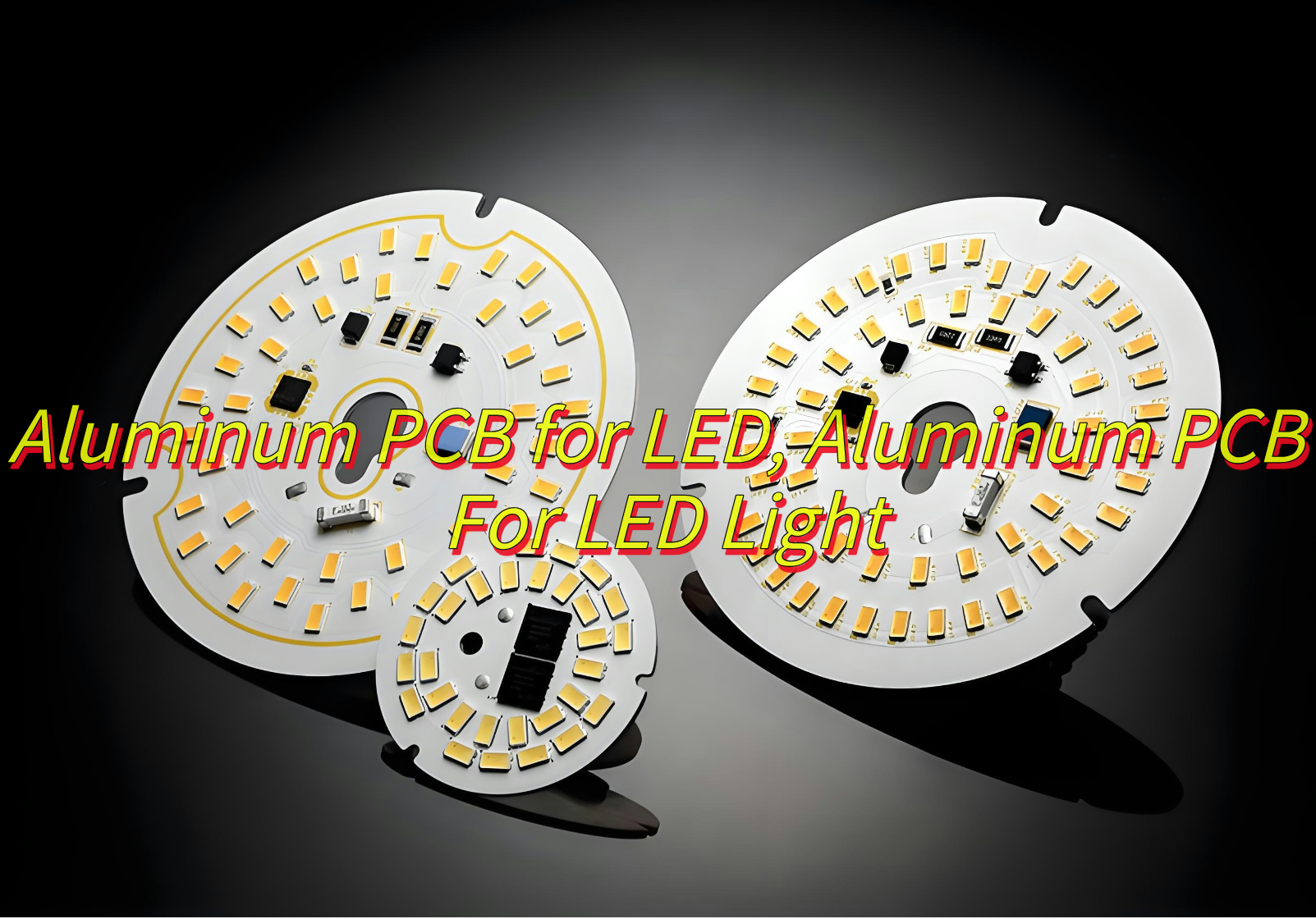
Are you looking for the best aluminum PCB for LED? Let’s Learn about its advantages, types , materials, design process and how to find a reliable PCB supplier.
At EBest Circuit (Best Technology), we focus on one stop aluminum PCB solution for LED, including aluminum LED PCB design, prototype and manufacturing. We have a stable supply chain and automated production lines that can achieve 72 hours fast delivery. And we have professional engineer teams who can provide you DFM analysis and free technical support to save production cost a lot. Feel free to contact us sales@bestpcbs.com if you have any request for aluminum LED PCB.
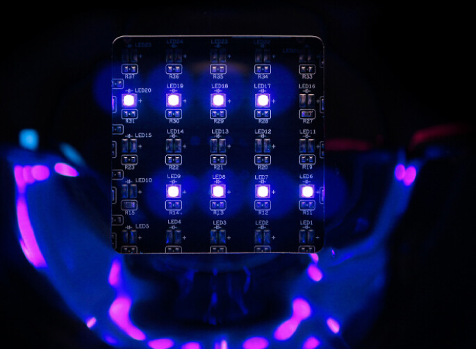
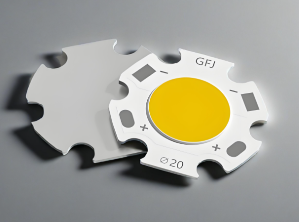
What is Aluminum PCB For LED?
Aluminum PCB for LED is a metal-based printed circuit board specifically designed for LED lighting. It achieves efficient heat dissipation by combining an aluminum substrate with insulating layers, ensuring the stable operation of high-power LED fixtures and extending their lifespan.
What Are the Advantages of Aluminum PCB For LED?
Here are main advantages of aluminum PCB for LED:
- Efficient heat dissipation: quickly export the heat generated by the LED, reduce the operating temperature and extend the service life.
- High current carrying capacity: carry higher current than traditional PCB at the same thickness, suitable for high-power scenarios.
- Lightweight: lightweight aluminum material, simplifying installation and reducing the overall weight of the equipment.
- Process compatibility: adapt to SMT mounting technology to simplify mass production process
- High mechanical strength: impact and vibration resistance, adaptable to harsh working environments.
- Electromagnetic shielding: effectively reduce electromagnetic interference and improve circuit stability.
- High voltage resistance: support voltage above 3000V to ensure safe operation.
- Environmentally friendly and recyclable: aluminum material is non-toxic and recyclable, meeting environmental standards.
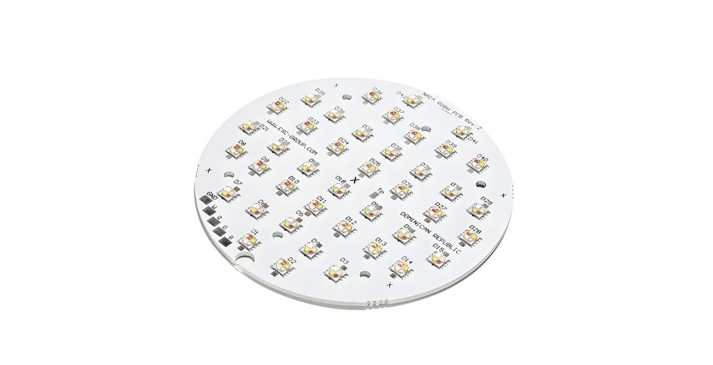
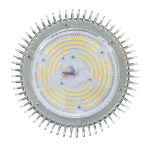
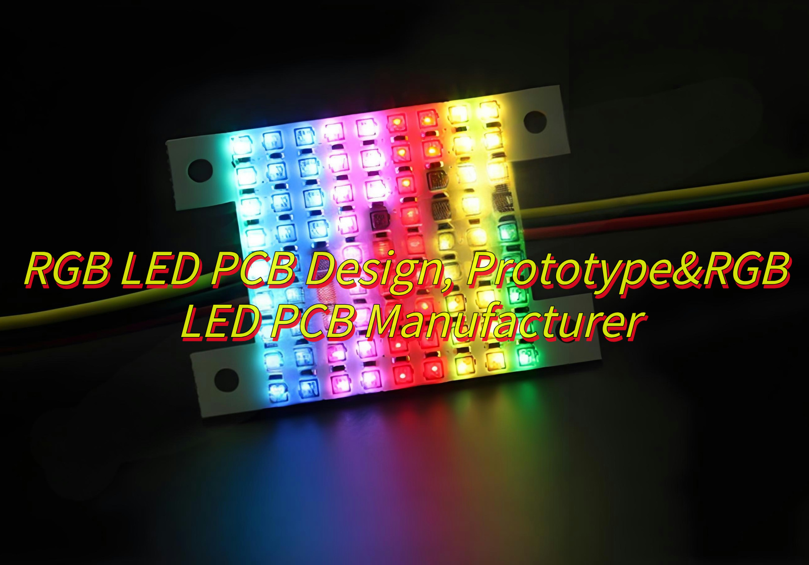
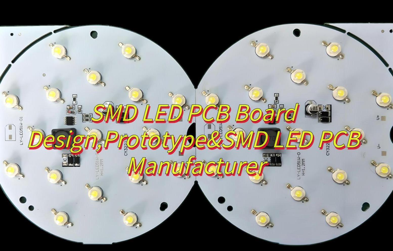
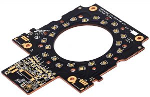
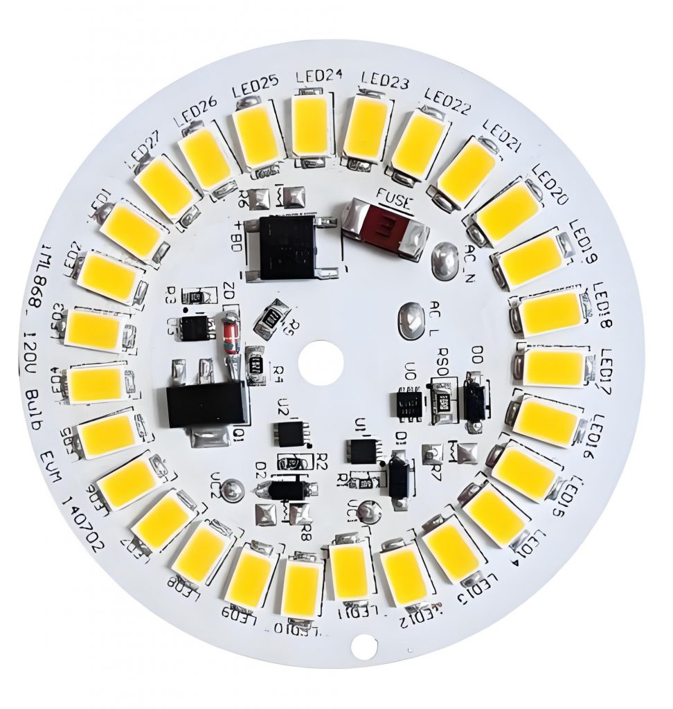
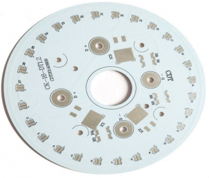
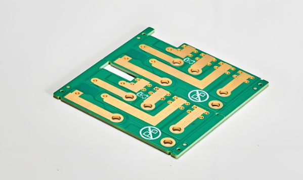
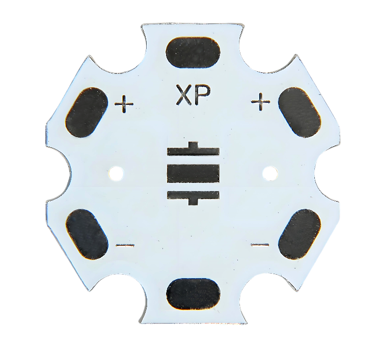
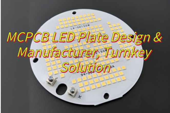
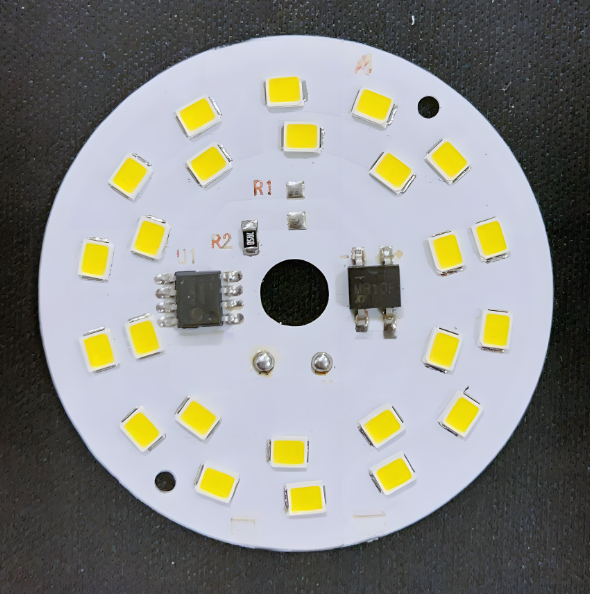
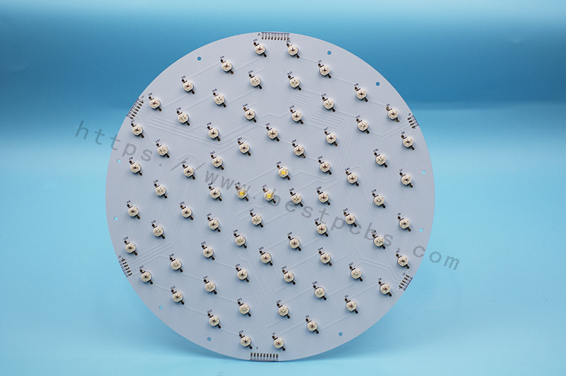
Aluminum PCB For LED
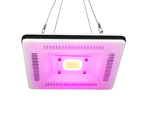
Application of Aluminum PCB For LED
Here are application of aluminum PCB for LED:
- LED bulbs-home and commercial lighting fixtures to prevent overheating and burning.
- Automotive lighting-headlights, brake lights, fog lights, high temperature resistance and vibration resistance.
- Advertising display screen-outdoor LED large screen, resistant to temperature changes and rain erosion.
- Industrial lighting-factory high-brightness searchlights, 24-hour stable operation.
- Medical equipment lights-surgical lights, detector light sources, fast heat dissipation to ensure safety.
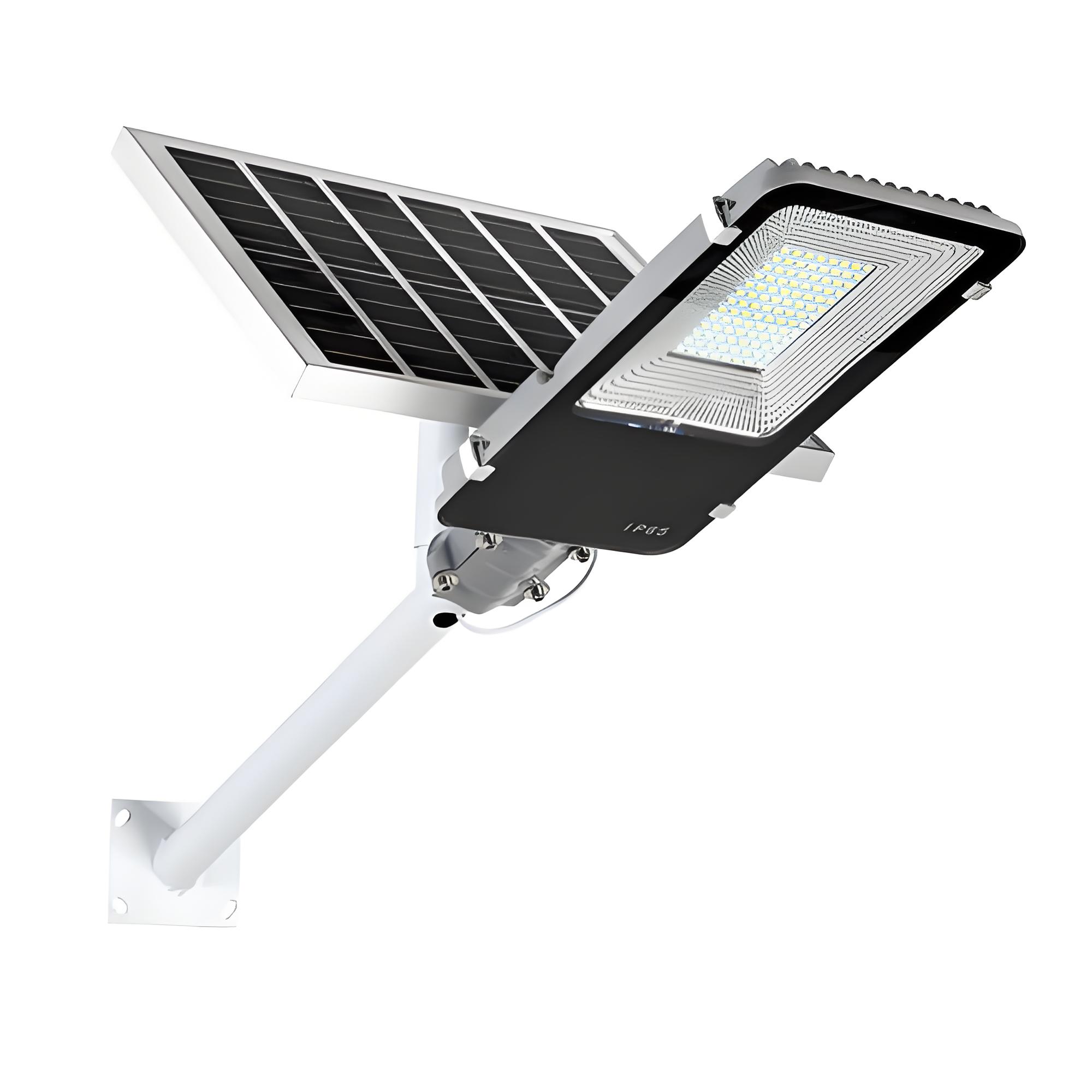
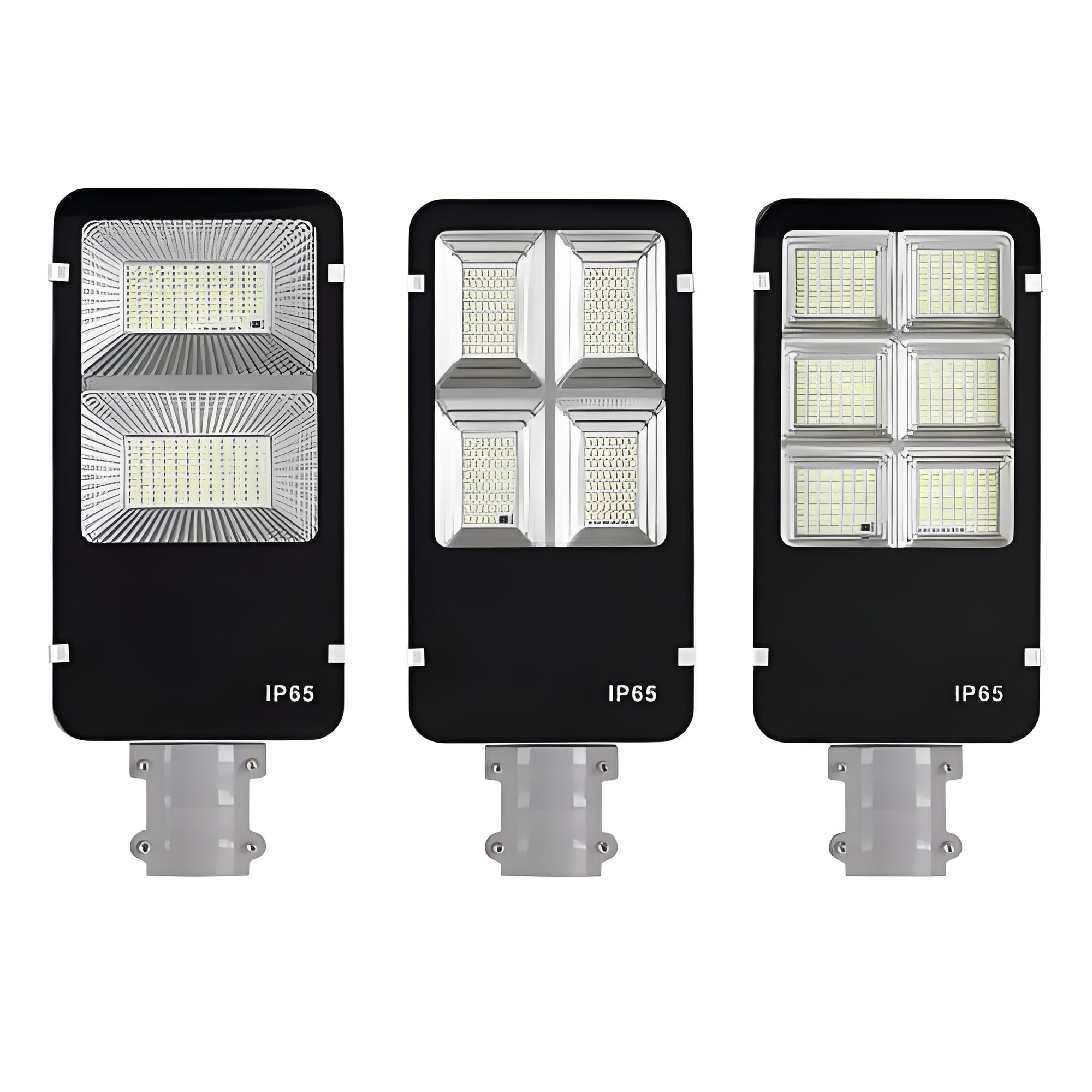
- Traffic lights-traffic lights, street lights, adapt to extreme weather.
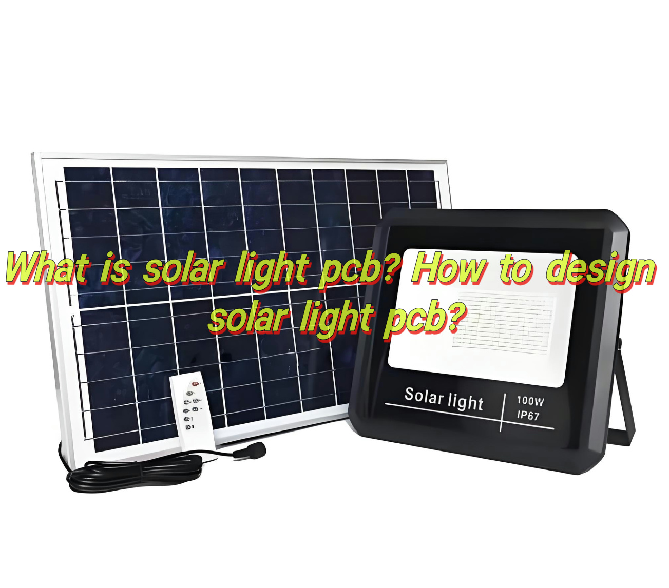
- Solar lights-garden lights, landscape lights, resistant to outdoor environment aging.
- Stage lighting– high-power spotlights.
- Household appliances– smart lamps, refrigerator backlight, thin and easy to install.
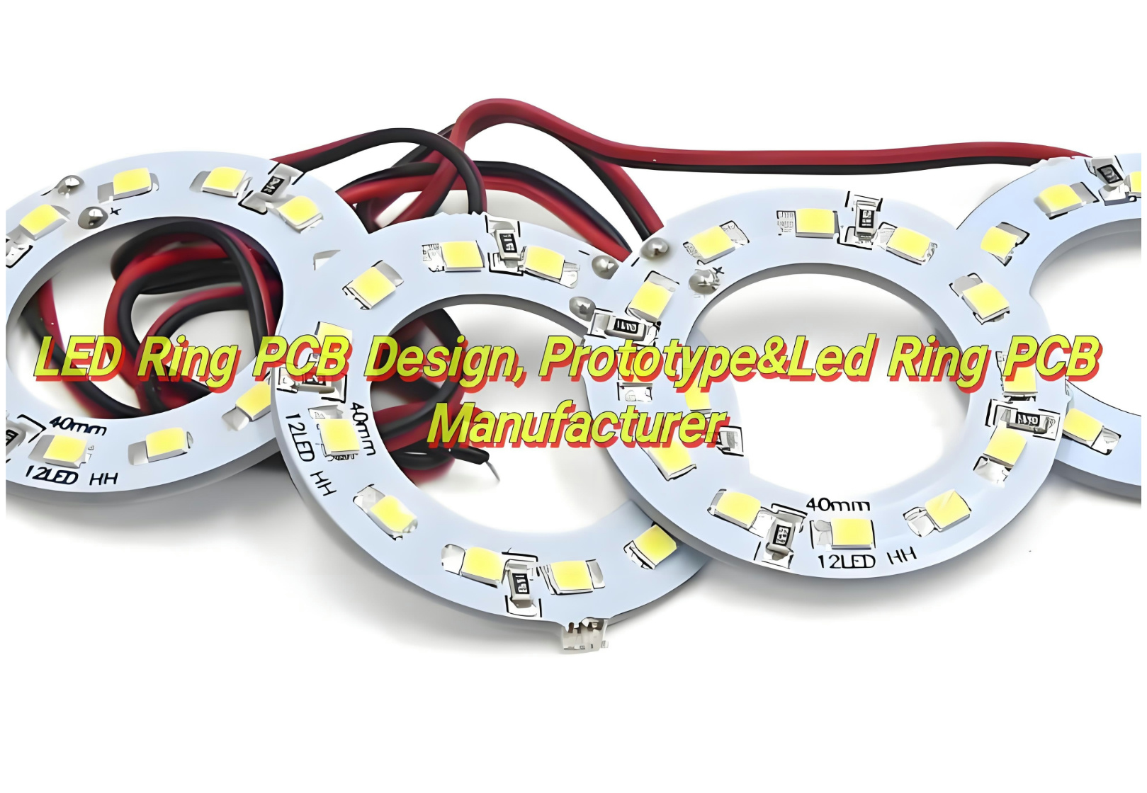
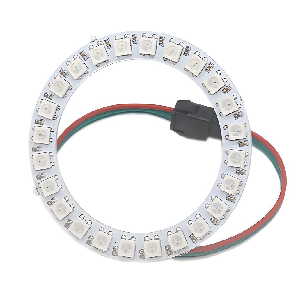
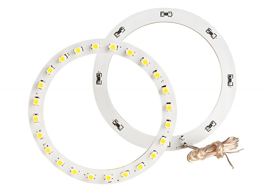
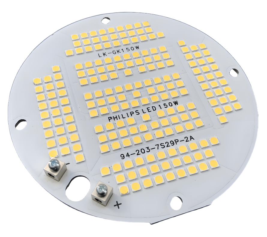
What Are the Types of Aluminum PCB For LED Light?
The aluminum PCB For LED light is divided into these types:
- Fluorescent lamp aluminum substrate: used for fluorescent lamps and other lighting equipment.
- Street lamp aluminum substrate: used for street lamps and other outdoor lighting equipment.
- Downlight aluminum substrate: used for downlights and other embedded lighting equipment.
- Wall lamp aluminum substrate: used for wall lamps and other wall lighting equipment.
- Spotlight aluminum substrate: used for spotlights and other directional lighting equipment.
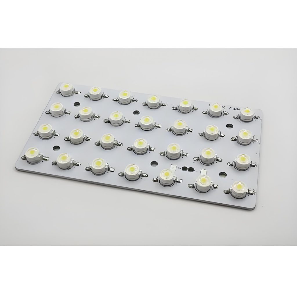
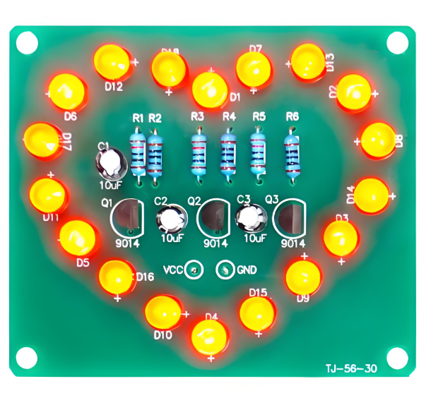
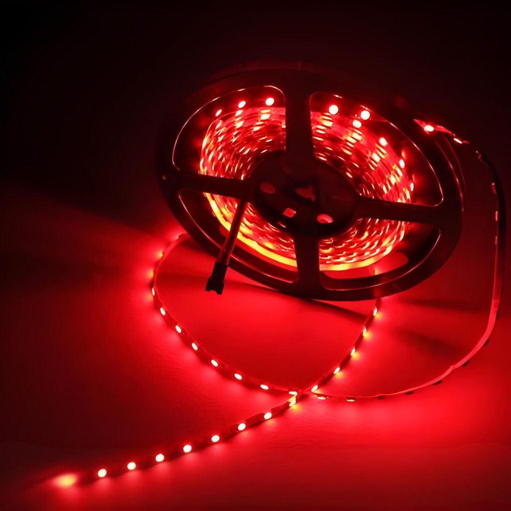
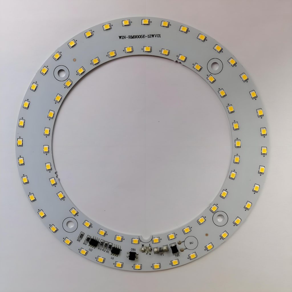
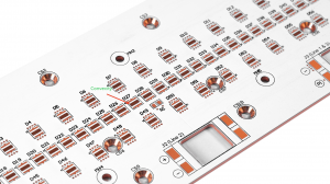
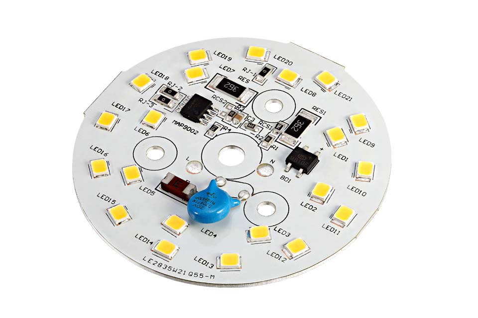
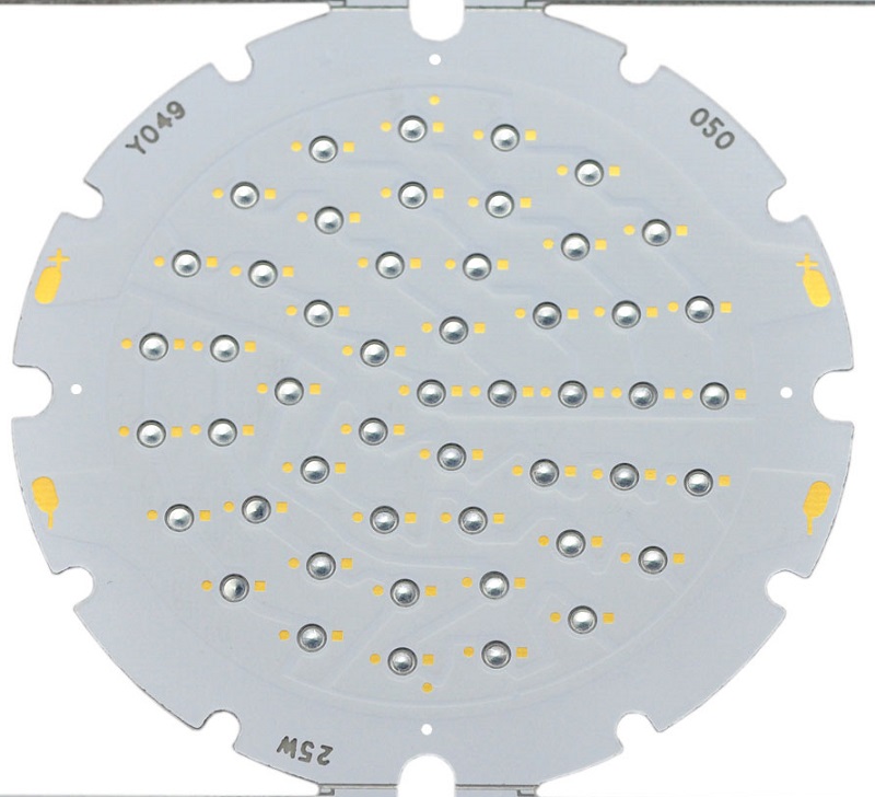
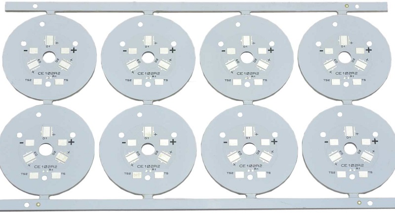
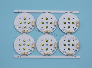
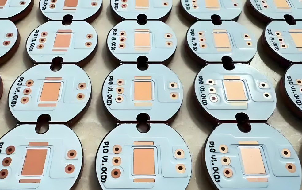
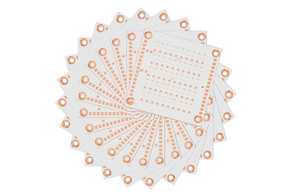
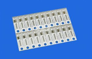
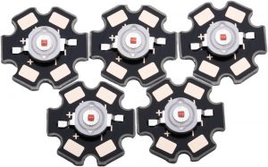
Aluminum PCB For LED Light
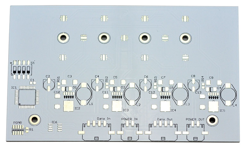
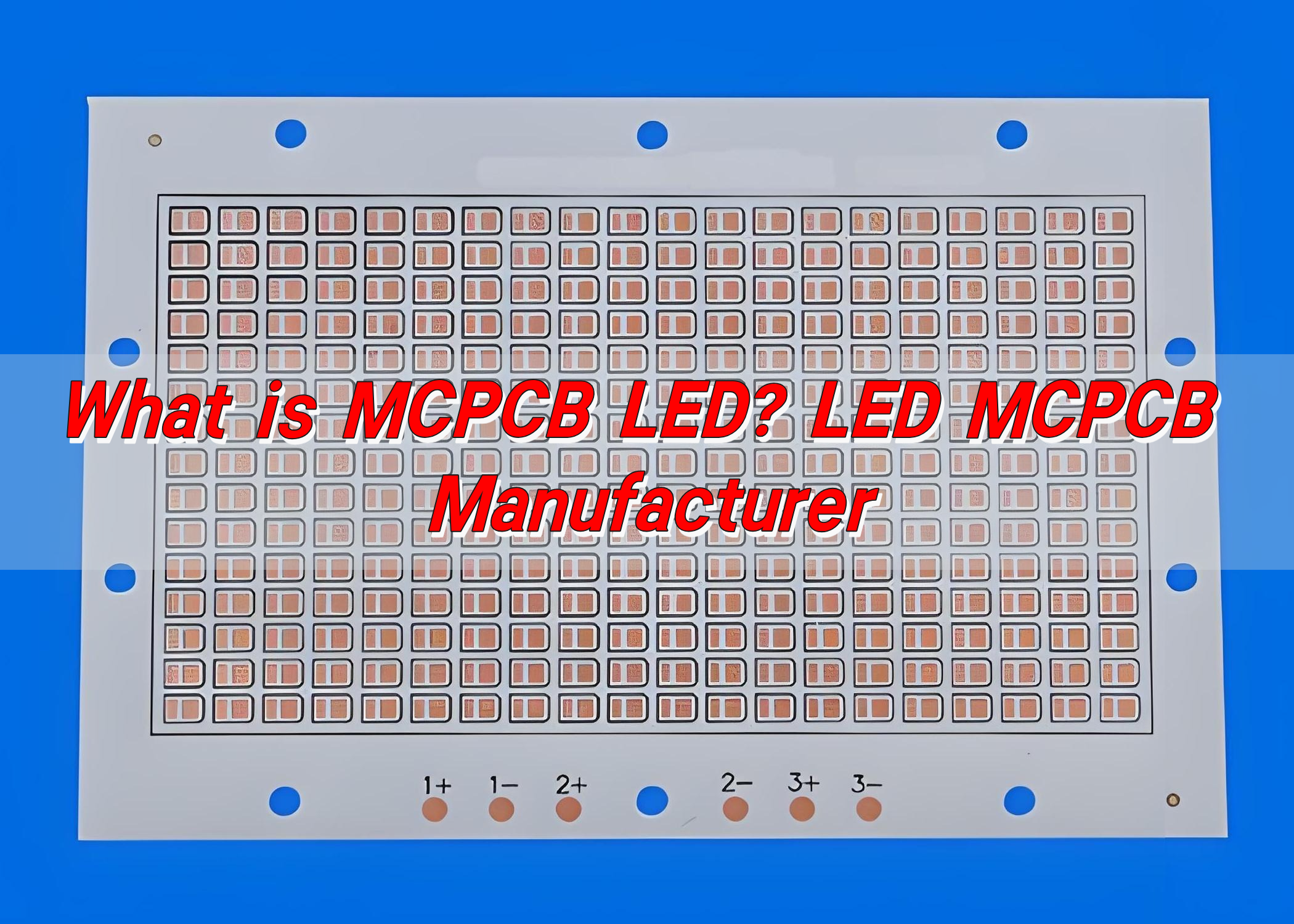
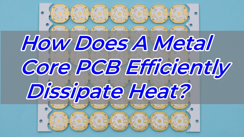
Aluminum PCB Board For LED Manufacturer
When uneven heat dissipation of LEDs causes accelerated light decay and a halved lifespan – what you lack is not just an aluminum substrate, but a full supply chain service from design to mass production! EBest Circuit (Best Technology) as an aluminum PCB board for LED manufacturer over 18 years who can provide you one-stop PCB solutions from design, prototype and production. Here are some information about our company:
- Made of high-quality aluminum raw materials, it has high thermal conductivity, fast heat dissipation, and extends the life of LEDs.
- With a stable supply chain and automated production lines, it can quickly respond to customer needs and achieve fast delivery (samples can be delivered in 72 hours at the fastest)
- Support DFM analysis, it can predict problems that may be encountered in the production process in advance during the design stage to reduce production costs a lot.
- Support low MOQ diversified customization services to create exclusive customization
- Provide free technical support, 24-hour professional engineer team will answer your questions online one-on-one.
If you’re interested in our services, welcome to leave a message below this blog.
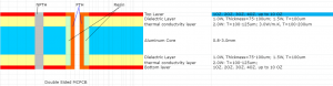
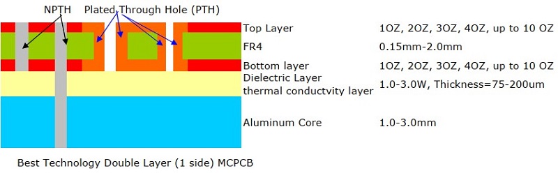
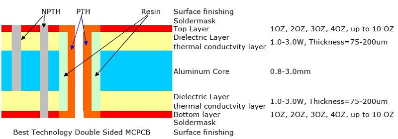
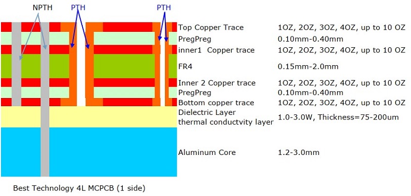
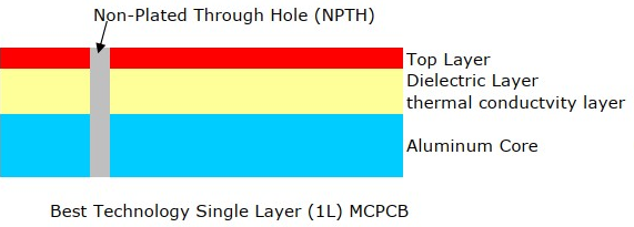
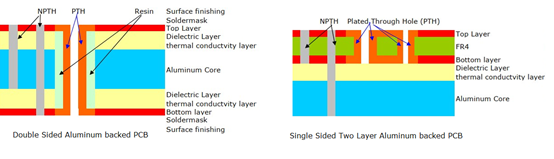
What Are the Materials of Aluminum PCB Board For LED?
Here are the materials of aluminum PCB board for LED:
- Substrate Layer–Aluminum(such as 6061 Aluminum alloy)
- Insulation layer–FR4 for normal thermal conductivity; ceramic powder mixture (such as alumina), silicone or special polymer for high thermal conductivity
- Conductive layer–Copper foil (1oz~6oz thickness), used for circuit routing.
- Surface treatment layer– OSP, HASL, silver/gold plating
- Additional coating–White solder mask ink (high reflection), black solder mask (anti-light interference)
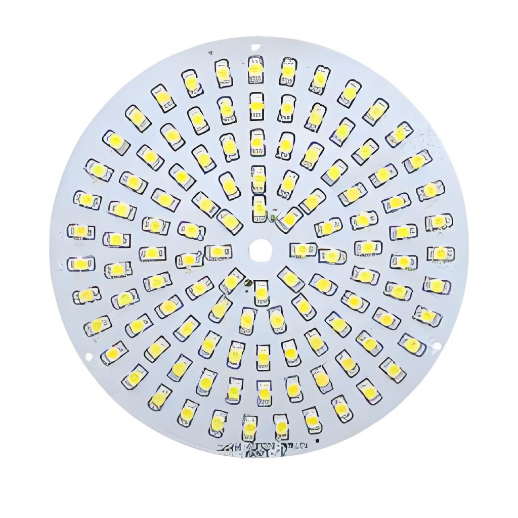
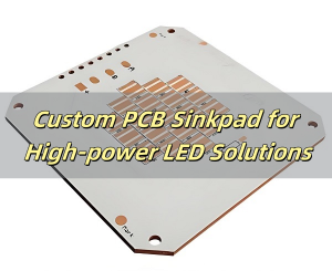
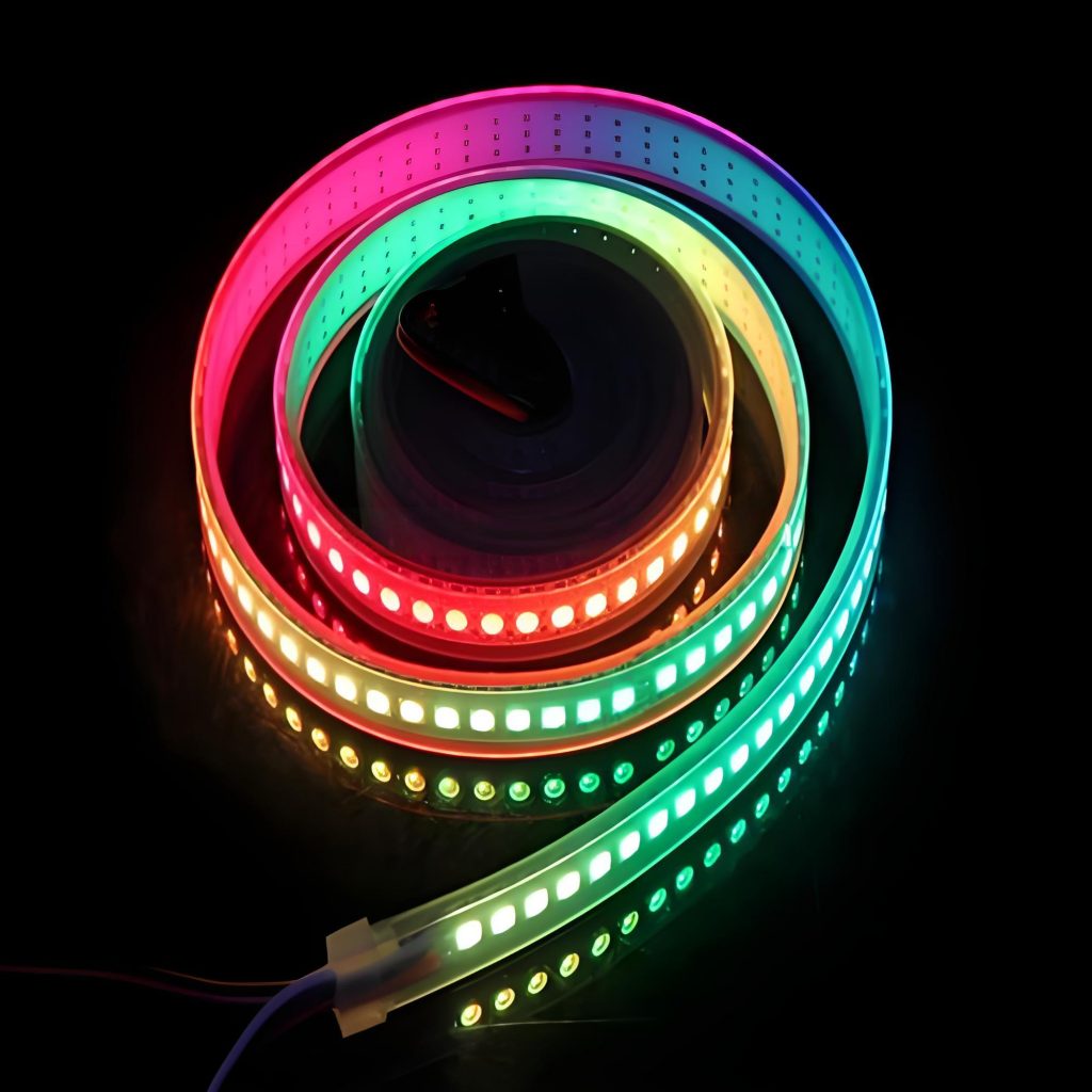
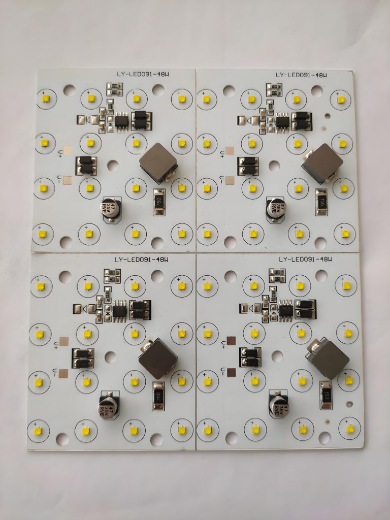
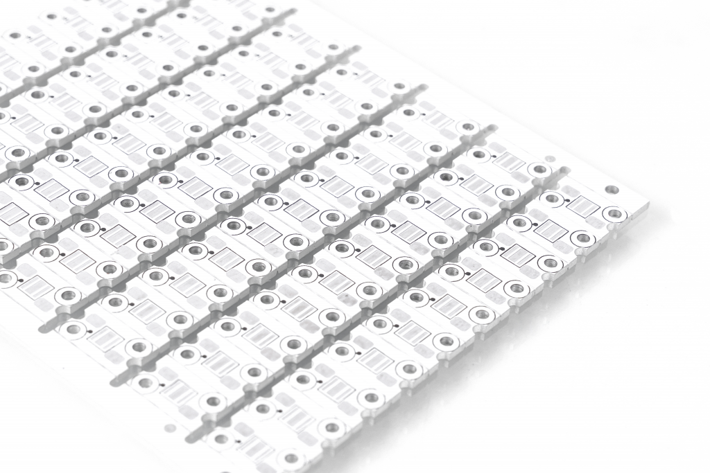
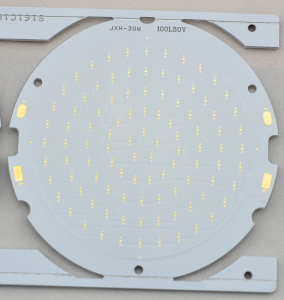
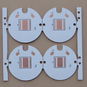
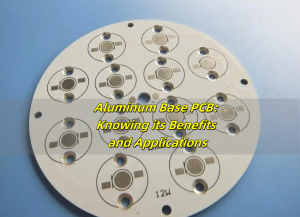
Aluminum PCB Board For LED
How to Design Aluminum PCB Board For LED?
Aluminum PCB for LED Design is mainly divided into five steps:
1. Basic design
- Select single/double-sided board: single-sided board (aluminum base + insulation layer + copper foil) for simple circuits, double-sided board for complex wiring.
- Aluminum base thickness: conventional 1.0~1.5mm, high power 2.0~3.0mm (such as 5052/6061 aluminum).
2. Circuit layout
- LED arrangement: evenly distributed, spacing ≥3mm (to prevent heat concentration).
- Line width calculation: Formula: Line width (mm) = current (A) / (copper thickness × 0.038).
- Wiring rules: Low voltage line spacing ≥ 0.2mm, high voltage (>50V) ≥ 1.0mm; Sharp angle routing is prohibited (arcs or 45° fold lines are preferred).
3. Pad design
- Size: 0.2~0.5mm larger than the LED pin (compatible with soldering process).
- Surface treatment: OSP is selected for general use, and immersion gold/silver plating is used for high reliability.
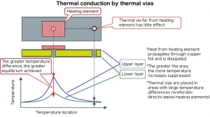
4. Thermal management
- Thermal conduction path: The aluminum base directly contacts the heat sink (insulating gasket is prohibited).
- Thermal resistance target: Total thermal resistance <5℃/W (high power requires <3℃/W).
- Verification method: Infrared thermal imager measures temperature rise (full load T<30℃).
5. Design output
- Gerber file: Insulation layer thickness, copper foil parameters, and Mark points are marked.
- DFM check: Line width error <±10%, pad and aluminum base edge >1mm.
FAQ of Aluminum PCB For LED
Q1: Why use aluminum PCB instead of FR4 for LED applications?
Aluminum PCBs offer superior heat dissipation, improving LED efficiency and longevity compared to FR4.
Q2: What is the typical thickness of an aluminum PCB for LED?
The standard thickness ranges from 1.0mm to 3.0mm, depending on application requirements.
Q3: Can aluminum PCBs be customized for different LED designs?
Yes, manufacturers like EBest Circuit (Best Technology) provide custom solutions for various LED applications.
Q4: How does aluminum PCB improve LED lifespan?
Efficient heat dissipation reduces LED degradation, ensuring consistent performance over time.
Q5: What surface finishes are recommended for aluminum PCB?
ENIG, HASL, and OSP are common surface finishes, each offering different benefits in terms of durability and solderability.
In conclusion, that’s all about aluminum PCB for LED. If you want to learn more, welcome to leave a message below this blog. Looking forward to your message!