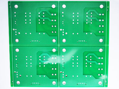
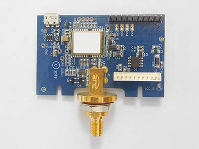
OEMs, especially those requiring only a few boards to be assembled, may want to outsource their Printed circuit boards to a professional PCB prototype assembler, rather than assemble the boards in-house. Instead of investing in expensive production equipment, they would prefer to obtain their product from a PCB prototype manufacturer, and have an expert assemble it, so that they have reliable PCBs. Fortunately, an eminent enterprise, EBest Circuit (Best Technology), provides expert solutions for both manufacturing and assembling PCBs.
OEMs are experts in the products they manufacture, but may not be so knowledgeable about the PCBs and assemblies that make up their product. Therefore, some guidelines are necessary to enable them select the professional PCB prototype assembler most suited to their requirements.
Technical Expertise
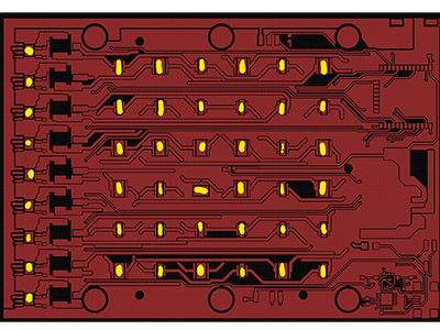
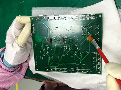
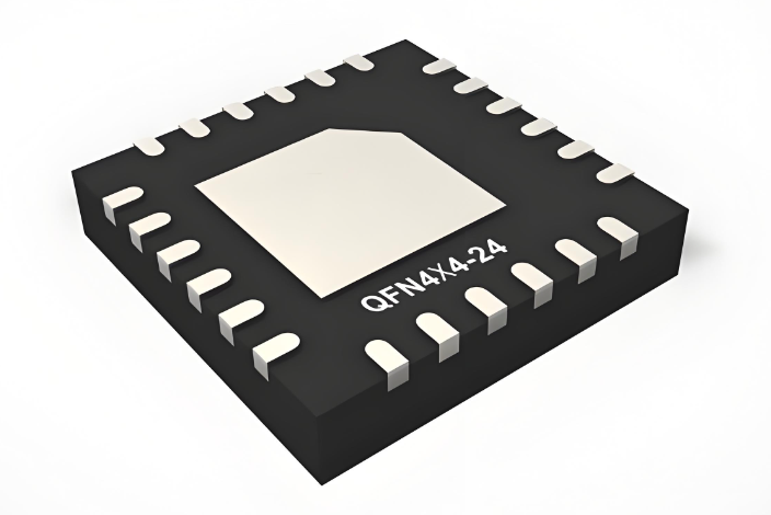
It is very important to ensure the assembler has the necessary processes in place. For instance, if the OEM requires BGAs on their PCB, they must ensure the assembler is capable of BGA assembly and rework, and they have X-ray machines for verifying their assembly. As most PCBs use surface mount devices, the assembler should be familiar with them to the extent of using automated machinery for SMT assembly.
Working Closely
If the OEM is outsourcing for prototype manufacturing and assembly, it is important that the assembler be willing to work with them for fixing errors in the layout, mistakes in the BOM, and parts that do not match the footprints on the board. The OEM should be able to make the most of the existing board while resolving the problems with the assembler.
Objective of the Outsourcing
To be effective, OEMs must also set their objectives that they expect from the outsourcing partner. This is important, as the objectives may vary. For instance, some may be planning to outsource a single product, others may be shifting their growing volumes to a partner with a higher production capacity, while still others may be looking for reducing costs.
Request for Quotation
When the OEM sends an RFQ or request for quotation to a PCB prototype assembler, it is important they provide all the commercial and technical information the assembler would need. This holds true even when the OEM is looking for a potential PCB prototype manufacturer.
Management Aspects
To ensure smooth working with the prototype assembler, it will be advantageous to the OEM if they periodically audit their partner, making sure the team has as wide range skills as possible. If necessary, the OEM can transfer some of their skills and knowledge to their partner. A good management practice is to establish regular meetings to make sure activities move on schedule, and the relationship can be discussed at higher levels, while the OEM outlines their strategic plans for the future.
Conclusion
EBest Circuit (Best Technology), both a professional PCB prototype manufacturer and a PCB prototype assembler, can handle not only prototype jobs, but also take up regular production works and turnkey projects. It meets all the above criteria, has the necessary quality management systems in place, and has the necessary technology and expertise to handle the most complicated board assemblies.