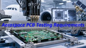
Printed circuit board inspection is the process of checking PCB quality before, during, and after manufacturing or assembly. It helps confirm that the board matches the design files, IPC requirements, customer specifications, and the real operating needs of the final product.
At EBest Circuit (Best Technology), printed circuit board inspection is handled as part of the full manufacturing workflow. With 20 years of PCB and PCBA manufacturing experience, our team combines DFM review, fabrication control, AOI, X-ray inspection, electrical testing, and assembly quality checks to support reliable production from prototype to mass production. If you are looking for a PCB or PCBA manufacturing partner with reliable inspection and full-process quality support, please feel free to send your Gerber files, BOM, and assembly drawings to sales@bestpcbs.com. Our engineering team will be glad to review your project requirements and provide suitable manufacturing support.
What Is Printed Circuit Board Inspection?
Printed circuit board inspection is a quality control process used to examine whether a PCB or PCBA meets the required design, manufacturing, and assembly standards. It may be applied to bare PCBs, assembled circuit boards, first article samples, incoming boards, or finished electronic modules.
For bare PCBs, inspection usually focuses on the board structure and fabrication quality. This includes board dimensions, layer count, copper thickness, hole size, solder mask alignment, surface finish, silkscreen clarity, routing accuracy, impedance requirements, and electrical continuity.
For PCB assembly, inspection becomes more component-focused. The factory checks whether each component is placed correctly, soldered properly, and free from visible or hidden defects. SMT placement, polarity, BGA soldering, through-hole solder joints, connector alignment, and cleanliness are all important checkpoints.
In simple terms, PCB inspection answers four important questions:
- Does the board match the Gerber files, BOM, and assembly drawings?
- Are there any visible or hidden defects?
- Can the board pass electrical and functional requirements?
- Is the product ready for shipment or the next production stage?
A good inspection process should not rely on only one method. Visual inspection, AOI, X-ray inspection, electrical testing, and functional testing all serve different purposes. When used together, they give a more complete view of board quality.
What Should Be Included in a Printed Circuit Board Inspection Checklist?
A printed circuit board inspection checklist should cover the most important items that affect PCB reliability, assembly yield, and final product performance. The checklist can vary depending on board type, industry, material, and application, but several core items are commonly used in professional PCB and PCBA production.
For bare PCB inspection, the checklist usually includes:
| Inspection Item | What to Check |
|---|---|
| Board dimensions | Length, width, thickness, outline, tolerance |
| Layer structure | Layer count, stack-up, dielectric thickness |
| Copper quality | Copper thickness, trace width, spacing, plating quality |
| Holes and vias | Hole size, via quality, annular ring, plugging, plating |
| Solder mask | Registration, color, coverage, opening accuracy |
| Silkscreen | Text clarity, polarity marks, component reference marks |
| Surface finish | ENIG, HASL, OSP, immersion silver, or other finish quality |
| Electrical performance | Open circuit, short circuit, continuity, impedance where required |
| Appearance | Scratches, stains, oxidation, delamination, warpage |
For PCBA inspection, the checklist should also include:
| Inspection Item | What to Check |
|---|---|
| Component placement | Correct part, correct position, correct orientation |
| Solder joints | Solder volume, wetting, bridging, insufficient solder |
| Polarity | Diodes, LEDs, ICs, electrolytic capacitors, connectors |
| Fine-pitch parts | Lead alignment, solder bridging, tombstoning |
| BGA and QFN packages | Hidden solder joints, voids, opens, shorts |
| Through-hole parts | Pin insertion, solder fillet, pin length |
| Cleanliness | Flux residue, solder balls, foreign particles |
| Labeling | Barcode, serial number, revision, traceability information |
| Functional result | Whether the assembled board performs as required |
The checklist should be clear enough for operators, inspectors, and engineers to follow. It should also match the product’s risk level. A simple consumer control board may need standard checks, while a medical device PCBA or automotive control board may require stricter documentation, traceability, and testing control.
What Are the Key Printed Circuit Board Inspection Criteria?
Printed circuit board inspection criteria are the standards used to judge whether a PCB or PCBA is acceptable. In professional manufacturing, the inspection team should not make decisions based only on personal experience. They need defined acceptance criteria.
Common inspection criteria include IPC standards, customer drawings, Gerber files, assembly drawings, BOM, test procedures, approved samples, and internal quality documents.
For bare PCB fabrication, common criteria may include:
- Correct board material and thickness
- Correct copper weight
- Accurate hole size and location
- Proper plating thickness in through holes
- Clean solder mask registration
- No open circuits or shorts
- Controlled impedance within tolerance when required
- No delamination, blistering, serious scratches, or contamination
- Board warpage within acceptable range
For PCB assembly, common criteria may include:
- Correct component value and package
- Correct component direction and polarity
- Acceptable solder joint shape
- No solder bridging between pads
- No tombstoning, missing parts, or shifted components
- No cracked ceramic capacitors or damaged ICs
- Acceptable BGA void ratio based on product requirements
- Clean board surface after soldering
- Passed electrical or functional test
IPC-A-600 is often referenced for bare PCB acceptability, while IPC-A-610 is widely used for assembled board acceptability. For soldering workmanship, IPC J-STD-001 is also commonly used. In real production, these standards are often combined with customer-specific requirements.
The most important point is consistency. A good PCB manufacturer should apply the same inspection criteria across engineering review, production, quality control, and outgoing inspection. This helps avoid inconsistent judgment and reduces disputes after shipment.
How Is Incoming Inspection for Printed Circuit Boards Done?
Incoming inspection for printed circuit boards is the process of checking PCBs or components before they enter assembly or production. It is especially important when bare PCBs are produced in one facility and assembled in another, or when customers supply their own boards.
For PCB assembly projects, incoming PCB inspection helps confirm whether the bare boards are ready for SMT production. If board issues are found only after solder paste printing or reflow soldering, the cost of correction becomes higher.
A typical incoming inspection process may include:
- Checking the packing condition
- Confirming part number, revision, quantity, and date code
- Reviewing the certificate of conformity or quality report
- Checking PCB dimensions and thickness
- Inspecting solder mask and surface finish
- Checking warpage before SMT assembly
- Confirming panel design and fiducial marks
- Reviewing special requirements such as impedance, via plugging, or heavy copper
- Performing sample electrical checks if needed
For components used in PCBA production, incoming inspection may include label verification, moisture sensitivity level control, package condition, quantity confirmation, and traceability record review. For high-risk or high-value components, X-ray inspection, decapsulation, or functional testing may be used when required.
At EBest Circuit (Best Technology), incoming inspection is not treated as an isolated receiving step. Because our PCB fabrication and PCBA assembly are coordinated within the same manufacturing workflow, our engineering and production teams can connect bare board quality, assembly requirements, and project documentation before SMT production begins.
Before assembly starts, our team reviews the PCB, BOM, Gerber files, pick-and-place files, and assembly drawings together. This helps us check whether the fabricated boards match the assembly requirements and identify potential mismatches early, such as pad design issues, unclear polarity marks, unsuitable footprints, panel design concerns, fiducial problems, or component availability risks.
Incoming inspection is the first quality gate before assembly. At EBest Circuit (Best Technology), it works together with DFM review, production preparation, and process control. This integrated approach helps prevent unsuitable boards or incorrect materials from entering the SMT line, improves assembly yield, and supports more stable PCB and PCBA manufacturing quality.
What Is First Article Inspection for Printed Circuit Boards?
First article inspection, often called FAI, is the detailed inspection of the first completed board or first production batch before full-scale production continues. It is an important step in PCB assembly because it confirms whether the manufacturing setup is correct.
In PCB assembly, first article inspection usually checks whether the first assembled PCBA matches the BOM, placement file, assembly drawing, polarity requirements, and customer specifications. This is especially useful for new products, engineering changes, new suppliers, or production line transfers.
A first article inspection may include:
- BOM verification
- Component value confirmation
- Component orientation check
- Reference designator check
- Polarity confirmation
- SMT placement accuracy
- Solder joint inspection
- AOI result review
- X-ray inspection for BGA, QFN, LGA, or hidden solder joints
- Electrical test or functional test
- Label and revision confirmation
FAI is highly valuable because many assembly errors are setup-related. For example, a feeder may contain the wrong part, a component direction may be interpreted incorrectly, or a polarity mark may be unclear on the silkscreen. If this type of issue is not found during the first article stage, the same defect may repeat across the whole batch.
For high-reliability products, first article inspection also supports documentation and traceability. It provides a record that the first build was reviewed and approved before volume production moved forward.
EBest Circuit (Best Technology) uses first article inspection as part of PCBA quality control for prototype, small-batch, and production projects. For complex boards, especially those with BGA, fine-pitch ICs, mixed SMT and through-hole parts, or special materials, FAI helps engineers and customers confirm the build before scaling up.
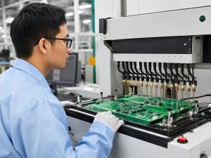
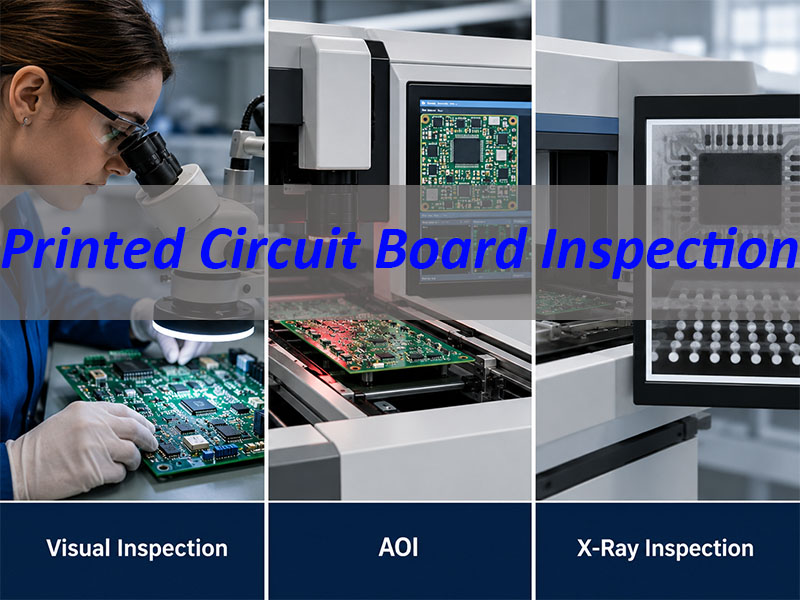
How Do Visual Inspection, AOI, and X-Ray Inspection Work in PCB Assembly?
Different inspection methods are used at different stages of PCB assembly. Each method has its own role. A strong quality control process does not depend on only one inspection tool.
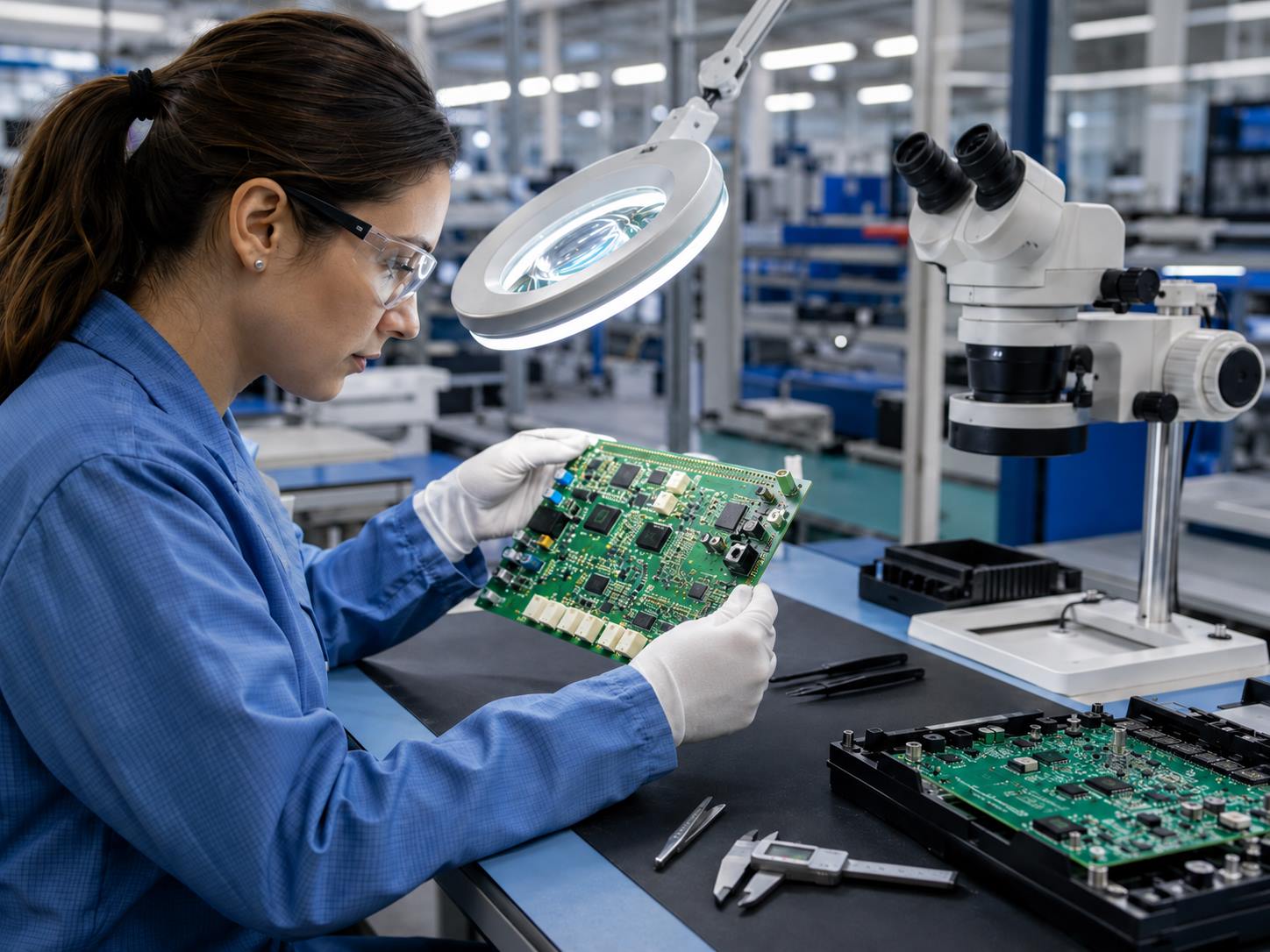
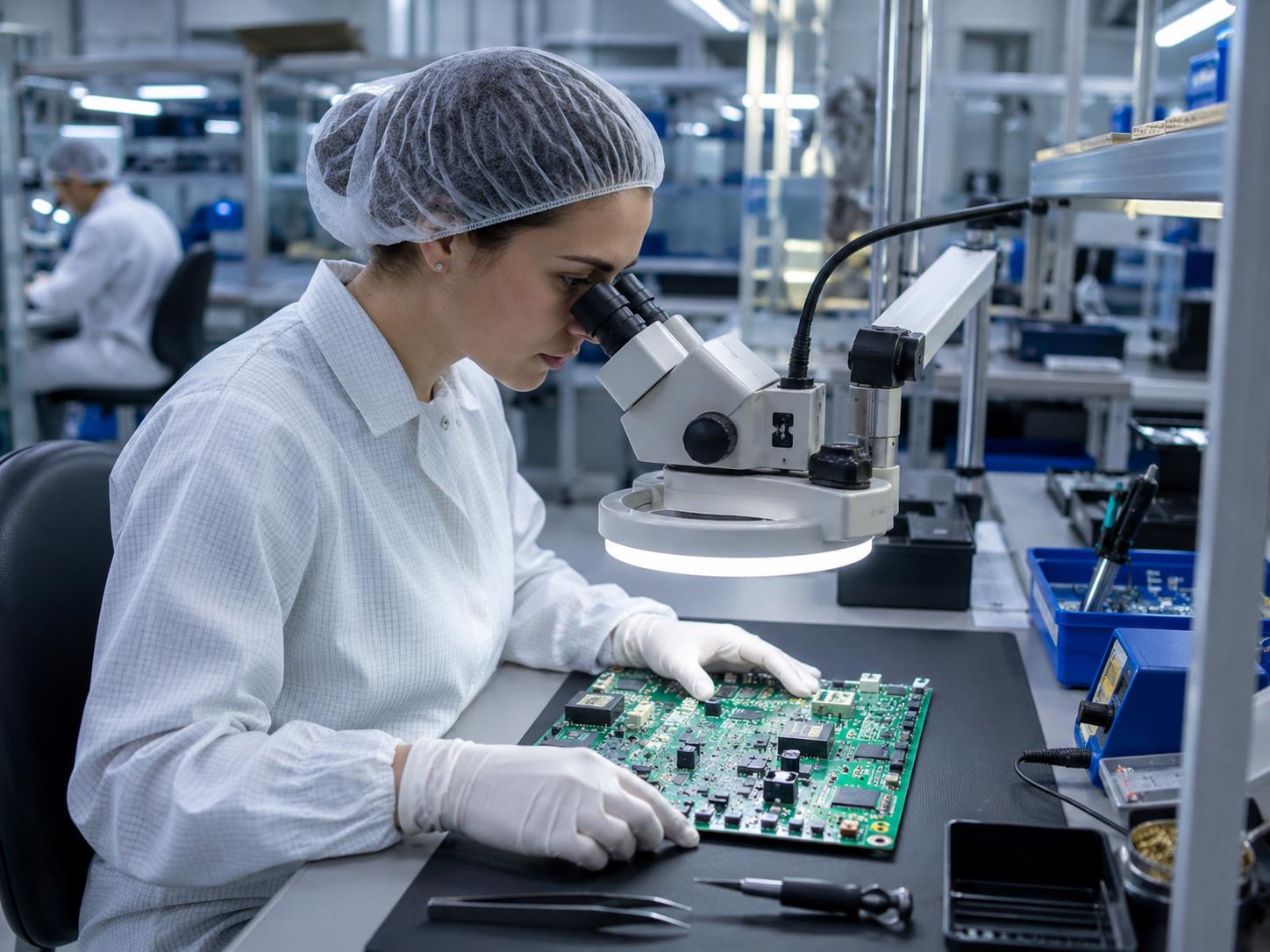
Visual inspection is usually performed by trained inspectors. It is useful for checking obvious assembly issues, solder joint appearance, component polarity, connector alignment, solder balls, contamination, broken parts, and board handling damage.
Visual inspection is flexible and practical, especially for prototypes and small-batch production. However, it depends on human judgment and cannot fully detect hidden solder defects under BGA, QFN, LGA, or bottom-terminated components.
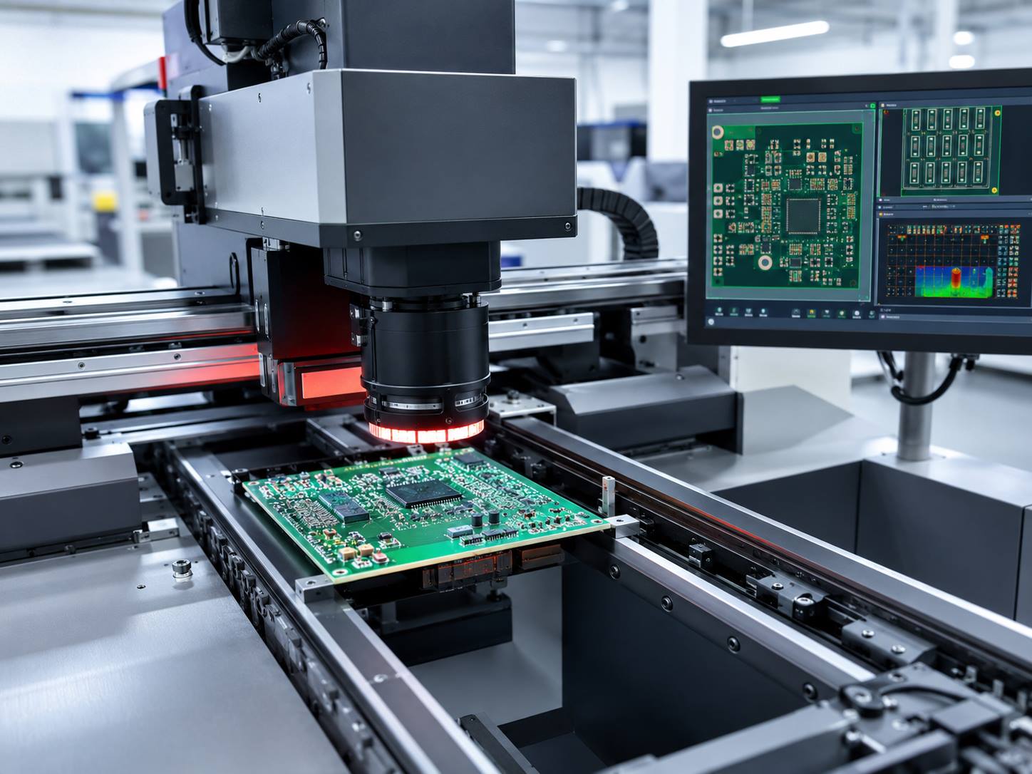
AOI, or automatic optical inspection, uses cameras and image analysis to inspect assembled boards. It is commonly used after SMT placement and reflow soldering. AOI can detect missing components, wrong polarity, component shift, tombstoning, solder bridging, insufficient solder, and some solder joint defects.
AOI is faster and more consistent than manual inspection. It is very useful for repeated production because the inspection program can compare each board against the approved standard. For boards with many small SMT parts, AOI improves inspection speed and reduces human error.
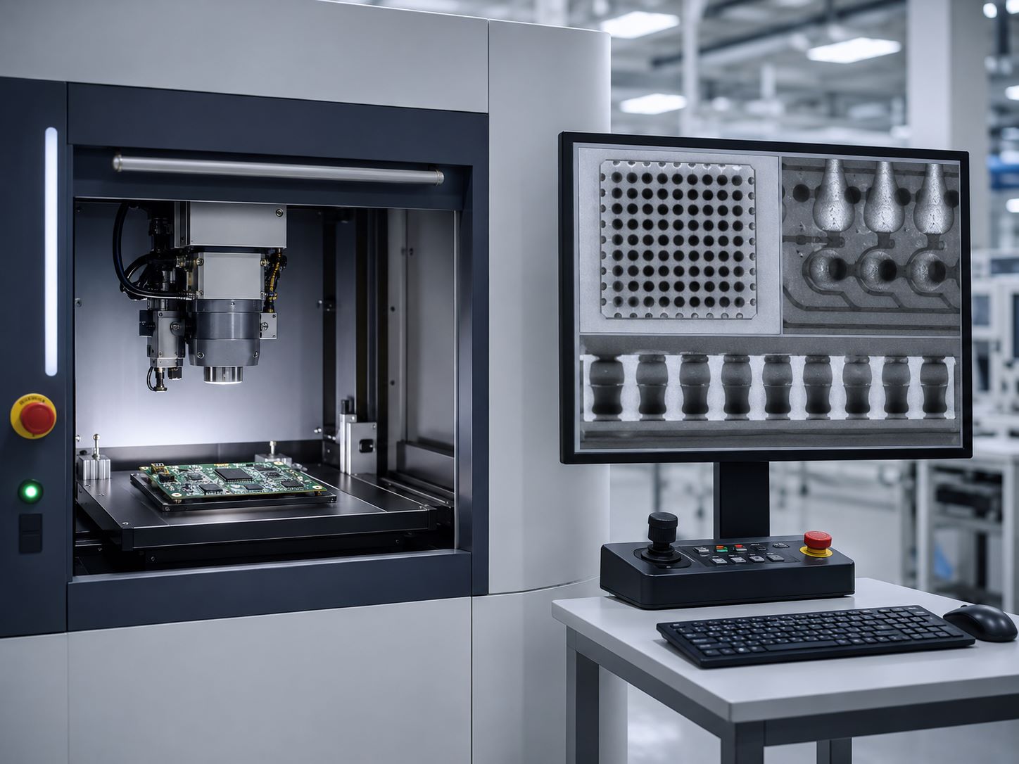
X-ray inspection is used when solder joints are hidden under the component body. It is commonly applied to BGA, QFN, LGA, bottom-terminated components, power devices, and some high-density PCB assemblies.
X-ray inspection can help detect:
- BGA solder voids
- Hidden solder bridges
- Open solder joints
- Head-in-pillow defects
- Insufficient solder under hidden pads
- Misalignment of hidden solder balls
- Internal connection problems
For advanced PCB assembly, AOI and X-ray often work together. AOI checks visible defects quickly, while X-ray checks areas that optical inspection cannot see. Electrical testing and functional testing can then verify whether the circuit works as intended.
EBest Circuit (Best Technology) applies suitable inspection methods based on product structure, component package, and customer requirements. A simple LED PCB may not require the same inspection plan as a medical PCBA or an automotive electronic control board. The inspection method should match the risk level of the product.
What Defects Can Be Found During Printed Circuit Board Defect Inspection?
Printed circuit board defect inspection helps identify problems that may affect assembly yield, electrical performance, or long-term reliability. These defects may come from PCB fabrication, component mounting, soldering, handling, or material storage.
For bare PCBs, common defects include:
| Defect Type | Possible Impact |
|---|---|
| Open circuit | Circuit path cannot conduct properly |
| Short circuit | Unwanted connection between traces or pads |
| Poor plating | Weak via or through-hole reliability |
| Solder mask misalignment | Soldering difficulty or exposed copper |
| Delamination | Reduced mechanical and thermal reliability |
| Warpage | SMT placement and soldering issues |
| Oxidation | Poor solderability |
| Incorrect dimensions | Assembly fit problems |
| Impedance deviation | Signal integrity issues in high-speed designs |
For PCB assembly, common defects include:
| Defect Type | Possible Impact |
|---|---|
| Missing component | Circuit function failure |
| Wrong component | Incorrect electrical behavior |
| Reversed polarity | Component damage or board failure |
| Solder bridge | Short circuit |
| Insufficient solder | Weak solder joint or intermittent failure |
| Tombstoning PCB | Open circuit on small passive components |
| Cold solder joint | Poor electrical and mechanical connection |
| BGA voiding | Reduced thermal or electrical reliability |
| Component shift | Poor contact or assembly failure |
| Flux residue | Cleanliness or reliability concern in sensitive products |
Some defects are easy to see. Others are difficult to detect without proper equipment. For example, a solder bridge between fine-pitch IC pins may be visible under magnification, but a head-in-pillow issue under a BGA may require X-ray inspection.
Defect inspection should also connect with root cause analysis. Finding a defect is only the first step. The factory should understand why the defect happened. Was the solder paste stencil opening unsuitable? Was the reflow profile incorrect? Was the PCB surface finish oxidized? Was the component moisture-sensitive and not stored properly?
A mature PCB manufacturer uses inspection results to improve the process. This is where manufacturing experience becomes important. The real value is not only detecting problems, but also preventing the same problems from repeating in the next batch.
FAQs About Printed Circuit Board Inspection
1. Why is printed circuit board inspection important?
Printed circuit board inspection helps detect fabrication and assembly defects before the product reaches the customer. It reduces rework, improves reliability, and supports stable production quality.
2. When should PCB inspection be performed?
PCB inspection should be performed during incoming material control, bare board fabrication, first article inspection, PCB SMT assembly, soldering, testing, and final outgoing quality control.
3. What is the difference between PCB inspection and PCBA inspection?
PCB inspection usually refers to checking the bare printed circuit board. PCBA inspection checks the assembled board after components have been mounted and soldered.
4. What is included in a PCB inspection checklist?
A PCB inspection checklist may include board dimensions, copper thickness, hole quality, solder mask alignment, surface finish, electrical testing, component placement, solder joints, polarity, cleanliness, and final test results.
5. What is AOI in PCB assembly?
AOI means automatic optical inspection. It uses camera-based image analysis to check component placement, polarity, solder bridges, missing parts, tombstoning, and other visible assembly defects.
6. When is X-ray inspection needed for printed circuit boards?
X-ray inspection is used when solder joints are hidden under components, such as BGA, QFN, LGA, or other bottom-terminated packages. It helps detect hidden bridges, voids, opens, and alignment issues.
7. What standards are used for printed circuit board inspection?
Common standards include IPC-A-600 for bare PCBs, IPC-A-610 for assembled boards, and IPC J-STD-001 for soldering workmanship. Customer specifications may also apply.
8. Can inspection find all PCB defects?
No single method can find every possible defect. A reliable inspection plan often combines visual inspection, AOI, X-ray inspection, electrical testing, functional testing, and process control.
9. How does first article inspection help PCB assembly?
First article inspection confirms that the first assembled board matches the BOM, drawings, placement files, and quality requirements before full production continues. It helps prevent batch-level mistakes.
10. How can I choose a reliable PCB inspection and assembly partner?
Choose a manufacturer with PCB fabrication, PCBA assembly, DFM review, incoming inspection, AOI, X-ray inspection, electrical testing, functional testing, and traceability control. Experience with medical, industrial, automotive, aerospace, and communication electronics is also valuable for high-reliability projects.
Overall, printed circuit board inspection is not a single checkpoint at the end of production. It is a complete quality control system that runs through PCB fabrication, incoming material review, SMT assembly, soldering, testing, and final shipment.
For standard boards, inspection helps maintain stable production quality. For high-reliability products, it becomes even more important because small defects may affect safety, service life, and field performance.
EBest Circuit (Best Technology) supports PCB manufacturing and PCBA assembly with engineering-driven quality control. Our team provides DFM review, PCB fabrication, component sourcing, SMT assembly, AOI, X-ray inspection, electrical testing, functional testing, and final quality inspection for customers in medical electronics, industrial control, automotive electronics, communication equipment, aerospace, UAV, lighting, and other demanding industries.
If you are working on a PCB or PCBA project that requires reliable inspection, stable manufacturing, and full-process quality support, please feel free to send your Gerber files, BOM, and assembly drawings to sales@bestpcbs.com. Our engineering team will be glad to review your requirements and provide professional support for your project.