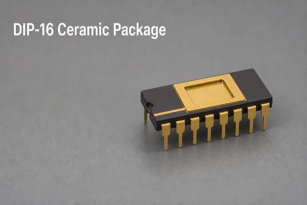
A DIP-16 ceramic package is a 16-lead, through-hole integrated-circuit package with two parallel rows of eight pins and a ceramic body. Engineers choose it when the device specification calls for ceramic construction, controlled sealing, thermal stability, long-term storage performance, or a qualified high-reliability package.
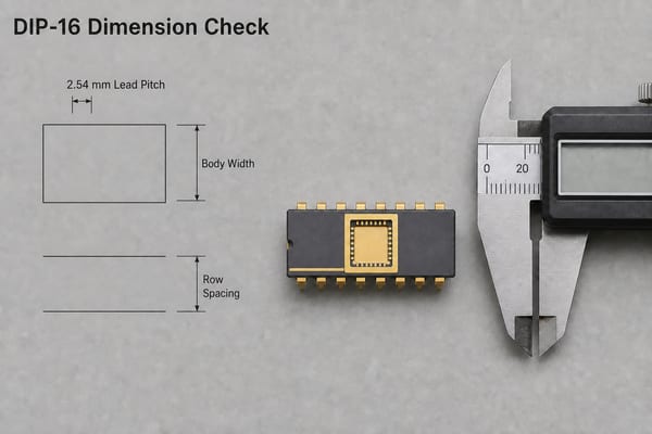
The name alone does not define every mechanical dimension or reliability grade. Lead pitch is commonly 2.54 mm, but body width, row spacing, lead shape, lid material, seal method, finish, temperature rating, and screening depend on the exact manufacturer drawing and part number. PCB designers and buyers should therefore treat the package drawing—not a generic DIP library—as the controlling source.
What Is a DIP-16 Ceramic Package?
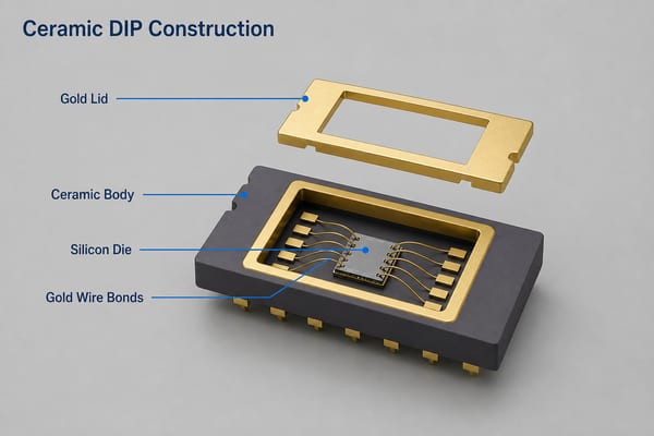
A DIP-16 ceramic package is a ceramic dual in line package with 16 external leads arranged as eight pins per side. The ceramic body protects the semiconductor die, while internal bond wires connect the die pads to the external lead system. A lid and sealing structure close the cavity in cavity-style packages.
The query what is dual in line package refers to the broader rectangular package form with two parallel lead rows. DIP describes that form factor; the number 16 gives the total pin count. Ceramic describes the body or package construction. A buyer searching for a ceramic dual in line package may still need to specify whether the device uses a metal-lid side-brazed structure, a glass- or frit-sealed CERDIP construction, or another vendor-defined ceramic package.
For a broader overview of package families, see our guide to IC package types and PCB footprints. The new design decision here is narrower: whether the exact 16-lead ceramic device drawing is compatible with the PCB footprint, assembly process, inspection plan, and procurement specification.
How Do DIP-16, CDIP-16, and CERDIP-16 Terms Differ?
DIP-16 defines the lead arrangement and pin count, while CDIP and CERDIP usually identify ceramic dual in-line package constructions. Vendor terminology is not perfectly uniform, so the package code on the datasheet must be tied to its mechanical outline and sealing description.
| Term | What It Identifies | What Still Needs Verification |
| DIP-16 | Two parallel rows with 16 total leads | Body material, width, row spacing, seal, finish, and qualification |
| CDIP-16 | A 16-lead ceramic dual in-line package designation | Side-brazed or other construction, lid and seal system, exact case outline |
| CERDIP-16 | A 16-lead ceramic DIP, often associated with a ceramic and glass- or frit-sealed construction | Manufacturer-specific seal process, moisture rating, temperature range, and screening |
| PDIP-16 | A 16-lead molded plastic DIP | It is not a drop-in ceramic substitute unless the electrical and mechanical specifications match |
Ceramic does not automatically mean hermetic, military-qualified, radiation-hardened, or suitable for every high-temperature application. Those claims require device-level documentation. The safest procurement wording names the manufacturer, full part number, package designator, drawing revision, lead finish, temperature grade, and any required screening or qualification.
DIP 16 Package Dimensions
The most common dip 16 package dimensions start with a 2.54 mm lead pitch and two rows of eight pins, but there is no single universal body outline. A 300 mil ceramic DIP family commonly uses approximately 7.62 mm nominal row spacing, while the body length, shoulder width, lead thickness, seating plane, and tolerances vary by package drawing.
| Dimension or Feature | Common Starting Point | Design Action |
| Lead count | 16 total, eight per side | Confirm numbering and pin-1 orientation on the device drawing |
| Lead pitch | 2.54 mm nominal is common | Use the drawing tolerance, not only the nominal library value |
| Row spacing | 7.62 mm nominal is common for a 300 mil style | Verify whether the drawing controls lead centers, body width, or both |
| Body length and width | Vendor- and construction-dependent | Build the courtyard and socket clearance from maximum dimensions |
| Lead section | Rectangular or formed lead geometry | Calculate the finished hole from maximum lead size and assembly allowance |
| Seating plane | Direct seating or controlled standoff | Check underside clearance, cleaning access, and mechanical stress |
Generic dip package dimensions are suitable for an early concept only. Before releasing Gerbers, compare the PCB footprint with the exact package drawing from the approved component manufacturer. Microchip publishes ceramic DIP drawings in its packaging specification, while Renesas provides a specific 16-lead ceramic metal-seal package drawing. These examples also show why one generic body-length value should not be applied to every source.
Which Materials, Lead Finishes, and Seals Are Used?
Ceramic DIP construction usually combines an alumina-based body, a conductive internal metallization system, a semiconductor die, bond wires, external alloy leads, and a lid or sealing layer. The exact materials affect thermal expansion, wire-bond compatibility, corrosion resistance, solderability, and storage requirements.
- Ceramic body: Provides dimensional stability, electrical insulation, and a low-permeability enclosure compared with molded plastic.
- Lead system: Iron-nickel or iron-nickel-cobalt alloys are common starting points, but the drawing or material declaration controls.
- Lead finish: Gold, nickel/gold, tin-based, or other finishes may be supplied. The selected finish must match soldering, wire-bond, storage, and compliance requirements.
- Bond wire: Gold or aluminum wire may connect the die to package pads, depending on the device process.
- Die attach: Eutectic, solder, or adhesive attachment may be used according to thermal and reliability needs.
- Seal: Metal-lid, brazed, glass, or frit-based structures are possible. Hermeticity must be confirmed from the package specification and test documentation.
Finish compatibility deserves special attention in repair and long-storage programs. Gold-plated leads, for example, may require a controlled gold-removal decision under the applicable assembly specification. Procurement should not substitute a different finish without engineering approval.
How Do Die Attach, Wire Bonding, and Hermetic Sealing Work?
The die is attached inside the ceramic cavity, bond wires connect it to metallized package pads, and the lid closes the cavity. In a hermetic design, the seal system is intended to limit gas and moisture ingress, but the actual performance depends on the construction, process controls, and verified leak-test requirements.
- The ceramic base receives its metallized conductors and external lead system.
- The semiconductor die is attached to the die pad using the specified material and cure or bonding process.
- Wire bonds connect die pads to the package terminals.
- Visual inspection checks die placement, bond placement, contamination, and obvious mechanical defects.
- The lid is sealed with the specified metal, glass, frit, or related sealing process.
- Electrical, seal, dimensional, and screening tests are applied as required by the device specification.
A ceramic enclosure protects the die; it does not eliminate electrical overstress, electrostatic discharge, cracked bonds, lid damage, corrosion, or assembly-induced failure. Device handling and board assembly controls remain necessary.
Which Package Drawings and Standards Should Engineers Check?
The controlling documents are the approved component datasheet, manufacturer package drawing, purchase specification, and applicable assembly standard. JEDEC outlines and military package case descriptions can help identify a family, but they do not replace the part-specific drawing.
- Mechanical package drawing: Lead pitch, row spacing, body envelope, lead section, seating plane, and tolerances.
- Device datasheet: Pinout, orientation, temperature range, electrical ratings, handling, and soldering limits.
- Package or case designation: JEDEC- or MIL-style references when the manufacturer provides them.
- Assembly requirements: The contractually specified edition of IPC J-STD-001, IPC-A-610, or customer workmanship criteria when applicable.
- Material and compliance records: Lead finish, substance declaration, storage condition, moisture or hermetic data, and traceability required by the purchase order.
Do not copy a footprint solely because two devices are both called CDIP-16. Match the full package designator and drawing dimensions. Also confirm whether the document shows the bottom view or top view before assigning pin numbers.
Where Are DIP-16 Ceramic Packages Used?
DIP-16 ceramic packages appear in equipment that values robust packaging, extended temperature options, long-term device storage, socketability, or qualified legacy components. Actual suitability comes from the complete device specification rather than the ceramic body alone.
- Industrial controls and instrumentation built around mature through-hole architectures.
- Test fixtures, development systems, and socketed devices that require replacement or programming access.
- Aerospace, defense, or high-reliability electronics when the exact device has the required qualification and screening.
- High-temperature or harsh-environment electronics when electrical ratings, package materials, and board design support the operating condition.
- Maintenance and redesign programs that must support an approved legacy package.
A plastic PDIP may share a similar footprint, but it is not automatically an acceptable replacement. Engineers must compare electrical performance, temperature rating, sealing, lead finish, mechanical envelope, qualification, lifecycle status, and system-level reliability.
What Should Engineers Check When Designing the PCB Footprint?
The PCB footprint should be built from maximum and minimum package dimensions, not from a nominal pin grid alone. The two lead rows must align without forcing the ceramic body or bending leads during insertion.
- Use two rows of eight plated through holes and mark pin 1 clearly on assembly and silkscreen layers.
- Set hole size from the maximum lead cross-section, insertion allowance, plating thickness, and fabrication tolerance.
- Choose annular rings that meet the board class, copper weight, drill tolerance, and rework needs.
- Provide enough courtyard for the maximum body, socket, extraction tool, adjacent components, and inspection access.
- Check copper clearance around each hole and decide whether thermal reliefs are appropriate for solderability and current.
- Keep routing and components away from the body area when a socket, standoff, or underside cleaning access is required.
- Review board thickness and hole aspect ratio if the assembly uses wave or selective soldering.
Our through-hole PCB design guide explains how finished-hole control, annular rings, component clearance, and assembly method affect manufacturability. Those checks are especially important when a brittle ceramic body must fit without lead stress.
How Should a DIP-16 Ceramic Package Be Assembled and Inspected?
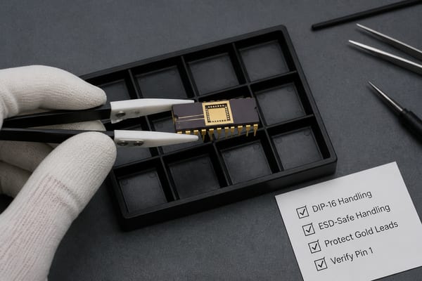
Assembly should protect the package from electrostatic discharge, lead deformation, excessive insertion force, thermal shock, and incompatible cleaning. A ceramic package may tolerate demanding environments in service, yet it can still crack or suffer seal and bond damage if handled poorly.
- Incoming inspection: Verify the part number, package code, date or lot traceability, lead finish, seal condition, pin-1 mark, and lead coplanarity.
- Footprint fit check: Test a representative component or approved gauge before production. Never force the two rows into a mismatched footprint.
- ESD-safe insertion: Align pin 1, support the board, and insert the device or socket evenly.
- Solder-process control: Apply the component manufacturer’s temperature and time limits. Tune wave, selective, or hand soldering to the board thermal mass.
- Cleaning: Confirm that the component, socket, markings, and seal are compatible with the cleaning chemistry and process.
- Post-solder inspection: Inspect fill, wetting, bridging, insufficient solder, lifted lands, contamination, lead damage, body cracks, and orientation.
- Electrical verification: Perform the required continuity, programming, functional, or system test after visual acceptance.
A socket can reduce heat exposure and simplify replacement, but it adds contact resistance, height, cost, and another mechanical interface. Direct soldering removes the socket interface but makes replacement and rework more difficult. Select the method from serviceability, vibration, reliability, and lifecycle requirements.
What Common Failures Should Designers and Buyers Prevent?
The most preventable failures come from wrong footprints, forced leads, incorrect orientation, unsupported substitutions, poor storage, and uncontrolled soldering. Ceramic construction does not compensate for a mismatched assembly process.
| Failure Mode | Likely Cause | Prevention |
| Lead bending or package stress | Incorrect row spacing or forced insertion | Verify the drawing, use a fit check, and control lead forming |
| Wrong circuit behavior | Pin-1 orientation or pinout error | Align schematic, footprint, silkscreen, assembly drawing, and inspection program |
| Weak or open solder joint | Wrong hole size, oxidized finish, insufficient heat, or poor flux access | Control finished holes, storage, solder profile, and joint inspection |
| Body or seal damage | Mechanical impact, clamping force, thermal shock, or aggressive rework | Use protected handling, supported insertion, and approved temperature limits |
| Field reliability mismatch | Assuming ceramic equals qualified or hermetic | Require the exact device grade, test evidence, and approved source |
| Early redesign or shortage | Obsolescence or single-source package dependency | Check lifecycle status and qualify alternatives before production need becomes urgent |
What Information Should Buyers Include in a DIP-16 RFQ?
A useful RFQ identifies both the component and the board-assembly requirements. “DIP-16 ceramic” alone leaves too many variables open and can lead to an electrically correct but mechanically or commercially unsuitable substitution.
- Manufacturer and complete component part number.
- Package designator and controlled mechanical drawing revision.
- Required temperature grade, qualification, screening, and traceability.
- Lead material and finish, including any solderability or gold-removal requirement.
- Approved alternates and the engineering change process for substitutions.
- Gerber or ODB++ data, drill files, fabrication drawing, assembly drawing, BOM, and centroid data where applicable.
- Direct solder or socket requirement, board quantity, prototype and production volumes, and test scope.
- Packaging, storage, date-code, shelf-life, and counterfeit-avoidance requirements.
If the component is obsolete or allocation-sensitive, ask for source traceability and do not authorize an alternate based only on the words “DIP-16.” Pinout, speed grade, temperature range, package seal, finish, dimensions, and qualification must all be reviewed.
FAQ About DIP-16 Ceramic Packages
1. Is every DIP-16 ceramic package hermetic?
No. Ceramic describes the package material or construction, while hermeticity is a verified package performance requirement. Confirm the seal type, package specification, leak-test requirement, and device documentation.
2. What Is a Dual In Line Package, and Does Every DIP-16 Use a 2.54 mm Lead Pitch?
A 2.54 mm pitch is common for standard dual in-line packages, but the approved mechanical drawing remains the authority. Do not release a footprint from the package name alone.
3. Can a ceramic DIP-16 replace a plastic PDIP-16?
Only after engineering verifies pinout, electrical ratings, timing, temperature range, body and lead dimensions, finish, qualification, and system requirements. A shared pin count does not make two devices equivalent.
4. Should a ceramic DIP-16 be socketed or soldered directly?
Use a socket when replacement, programming, or thermal isolation during assembly is important. Direct soldering may be preferable when contact interfaces, height, vibration, or cost are more critical. Evaluate the complete operating environment.
5. How is the correct plated-hole diameter selected?
Start with the maximum lead cross-section, then add insertion allowance and account for plating and drill tolerances. The PCB fabricator and assembler should review the finished-hole requirement together.
6. What should be inspected after soldering?
Check orientation, body and seal condition, lead damage, solder wetting, hole fill, bridging, contamination, lifted pads, and board damage. Complete the electrical or functional test required by the product plan.
How Can EBest Circuit Support a DIP-16 PCB Assembly?
A reliable DIP-16 assembly starts with the correct component drawing, plated-hole design, solder method, inspection criteria, and substitution controls. At EBest Circuit, we can review your PCB fabrication and PCBA package for through-hole or mixed-technology production. Send us the Gerber files, drill data, BOM, assembly drawing, package drawing, quantities, and test requirements so our engineering team can evaluate manufacturability and prepare a quotation at sales@bestpcbs.com.