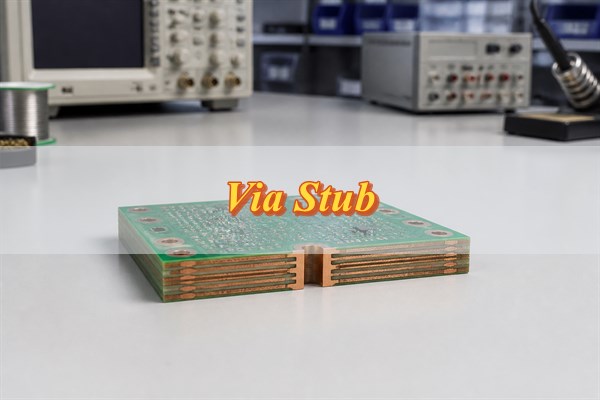
A via stub is the unused part of a plated through-hole that continues past the layer where a signal enters or leaves the via. Electrically, that unused copper barrel behaves like an open-ended transmission-line branch. It can reflect energy, create a sharp loss notch near resonance, and reduce eye margin even when the routed trace impedance is otherwise correct.
The practical question is not whether every stub is harmful. It is whether the residual length, dielectric environment, signal edge rate, via geometry, and channel loss place the disturbance inside the operating bandwidth. A useful review therefore connects the stackup and drill geometry to a frequency estimate, a field or S-parameter model, and measurable acceptance evidence.
What Is a Via Stub in a Multilayer PCB?
Consider a through-hole via that extends from the top surface to the bottom surface of a multilayer PCB. If a signal travels from the top layer to an inner layer, only the barrel between those two layers carries the intended signal transition. The unused plated section below the destination layer is the via stub. The same situation can occur from the opposite side or at both ends when a connection uses two internal layers.
The active via section and the stub are physically continuous, but they serve different electrical functions. Current follows the intended path into the destination trace. Part of the incident wave also enters the unused branch, reaches its open end, and reflects. That reflected energy returns to the junction with a frequency-dependent phase.
- Signal section: the barrel length required to connect the source and destination layers.
- Residual section: the unused plated barrel beyond the transition layer.
- Reference transition: nearby ground vias and return-path geometry that determine how the electromagnetic field crosses layers.
- Discontinuity region: the barrel, pads, anti-pads, and plane openings that together create the local impedance change.
Measure the electrical stub from the signal junction to the open plated end. Drill diameter does not define that length. Use the fabrication drawing, finished board thickness, connected layer pair, and planned backdrill depth to calculate the residual barrel.
Why Does the Via Stub Effect Harm Signal Integrity?
The via stub effect begins with an impedance discontinuity. At lower frequencies, the unused branch often appears mainly as additional capacitance and inductance around the transition. As frequency rises, phase delay along the branch becomes important. The returning reflection can reinforce or oppose the through signal, producing frequency-selective behavior rather than a simple broadband loss.
In a serial link, the visible symptoms depend on the channel and receiver, not on the stub in isolation. A return-loss peak may increase deterministic jitter. An insertion-loss notch can remove spectral energy required to form a fast edge. Multiple transitions can interact, and a connector or package resonance may hide or amplify the same defect.
- Reflection: energy returns toward the transmitter because the open branch does not absorb the wave.
- Ringing: repeated energy exchange around the discontinuity can create overshoot, undershoot, or settling errors in the time domain.
- Loss notch: destructive interaction at a particular frequency can produce a deep dip in insertion loss.
- Eye closure: reduced high-frequency content and added jitter shrink horizontal or vertical eye opening.
- Mode conversion: asymmetry between the positive and negative paths of a differential pair can convert differential energy into common-mode energy.
Data rate alone is not a sufficient screening value. Edge rate controls the useful spectral content, while coding, equalization, insertion loss, and receiver tolerance determine how much disturbance the link can accept. Review the highest significant channel frequency and the allowed loss or reflection mask rather than applying one universal Gbps threshold.
What Is Via Stub Resonance?
An open via branch produces its strongest first-order disturbance when its electrical length approaches one quarter of the guided wavelength. At its quarter-wave condition, the open stub transforms into a low-impedance disturbance at the junction. The through path can then show a pronounced insertion-loss notch and a return-loss peak.
This does not mean the copper barrel becomes a perfect textbook resonator. The via includes pad capacitance, anti-pad geometry, barrel inductance, plane coupling, losses, and a three-dimensional return path. Those features shift and damp the response. The quarter-wave relation is a screening estimate that tells the engineer where to investigate, not a substitute for a field model.
Longer unused via sections move the resonant disturbance to a lower frequency, as shown in Texas Instruments high-speed layout guidance. Shortening the residual barrel moves the first notch upward and reduces its effect within a fixed channel bandwidth.
How Do You Estimate Via Stub Resonance Frequency and Length?
A first-pass via stub resonance frequency estimate uses the quarter-wave relation:
fstub ≈ c / (4 × Lstub × √εeff)
Here, c is the speed of light in vacuum, Lstub is the residual barrel length, and εeff is the effective relative permittivity seen by the via field. The effective value is not automatically equal to the laminate’s catalog Dk. Resin distribution, glass weave, frequency, pads, anti-pads, and surrounding planes influence the field.
For a diagnostic example, assume a 5.0 mm residual section and an effective permittivity of 3.5. The estimate is approximately 8.0 GHz. If the channel must preserve useful energy near that range, the geometry deserves a more accurate model. This is an illustrative calculation, not a BestPCBS process limit or a universal pass/fail threshold.
| Input | What to Use | Common Error |
| Stub length | Distance from the signal transition layer to the open plated end | Using total board thickness |
| Effective permittivity | Value appropriate to the via field and frequency | Copying a low-frequency laminate Dk without review |
| Bandwidth | Channel requirement based on edge rate, modulation, and specification mask | Using bit rate as the only frequency |
| Acceptance margin | Allowed insertion loss, return loss, jitter, or eye penalty | Treating the estimated notch as an automatic failure |
A via stub calculator should therefore expose its assumptions. Use it to rank candidates, compare layer transitions, or set a maximum residual length for layout. Use a 3D field solver when the estimated disturbance approaches the operating band, when pad stacks change across layers, when multiple vias interact, or when the specification margin is small.
How Do Pad and Anti-Pad Dimensions Change a Stub Via?
The barrel is only one part of a stub via. A pad increases local capacitance, while an anti-pad controls the clearance between the via structure and adjacent reference planes. A smaller clearance generally increases capacitive coupling to the plane; a larger clearance can reduce that capacitance but may disrupt the return-current path or consume routing space.
Unused internal pads can also alter the response. Removing a nonfunctional pad may reduce capacitance, but the decision must account for fabrication rules, annular-ring requirements, registration tolerance, reliability, and the fabricator’s approved pad stack. Do not remove pads mechanically across every layer without a stackup-specific DFM review.
The Polar Instruments via impedance example illustrates why pad and anti-pad dimensions must be reviewed together. Its worked geometry is useful for understanding the direction of change, but it is not a universal dimensional recipe. For a high-speed differential transition, also check pair symmetry, ground-via placement, plane changes, and the spacing from each signal via to its return vias.
- Pad-stack audit: identify functional and nonfunctional pads on every layer.
- Anti-pad audit: verify clearance shape, size, and consistency through the reference planes.
- Return-path audit: confirm that stitching vias provide a short, symmetric path across reference changes.
- Differential audit: compare the two transitions for barrel length, breakout, pad stack, and nearby copper.
How Do You Model a Via Stub in ADS with S-Parameters?
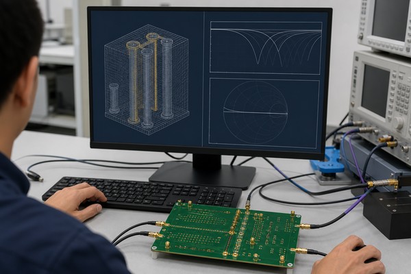
To model a via stub in ADS with S-parameters, treat the via region as a multiport interconnect rather than inserting a single lumped capacitor. Define ports at the trace interfaces, include the signal vias and relevant return vias, and preserve the actual layer stack, material properties, pad stacks, anti-pads, and conductor thicknesses.
- Define the model boundary: include enough trace on each layer to establish a stable reference plane without making the structure unnecessarily large.
- Assign ports: use a port arrangement that supports the intended single-ended or differential analysis and includes the return conductors.
- Extract the interconnect: generate broadband S-parameters from the via geometry with an appropriate electromagnetic solver.
- Check passivity and causality: reject or repair data that creates nonphysical gain or unstable time-domain behavior.
- Cascade the channel: insert the Touchstone block between package, connector, and trace models in the ADS channel schematic.
- Compare variants: sweep residual length, anti-pad, return-via position, and layer transition while keeping the rest of the channel constant.
Inspect mixed-mode insertion loss and return loss for a differential link, then correlate the frequency-domain result with the impulse response and eye simulation. Keysight’s de-embedding guidance is also relevant when a measured via coupon includes launches and fixtures that must be removed before model comparison.
How Does an SI9000 Via Stub Check Work?
An SI9000 via stub check is a fast screening step. The engineer supplies the residual length, dielectric information, and signal transition requirement or rise-time context. The tool estimates whether the unused section is likely to intrude into the permitted frequency range and presents a go/no-go style result.
Polar’s SI9000 documentation states the key trends: risk increases as the stub becomes longer or as dielectric loading increases, and faster signal edges make a given structure more critical. That relationship is useful during stackup planning because layer swaps can be evaluated before detailed routing is complete.
A screening result does not prove channel compliance. It does not automatically include every pad, anti-pad, return via, connector, package, plane cavity, or equalization setting. Use a failed screen to trigger geometry changes or detailed analysis. Use a passed screen as evidence that the simple length criterion is acceptable for the configured assumptions, then retain normal channel verification.
How Do You Eliminate the Via Stub Effect?
Reduce the via stub effect by shortening or removing the residual barrel, or by lowering the transition’s electrical sensitivity. Select the method from the required layer transition, routing density, fabrication flow, reliability requirements, and cost target.
- Move the routing layer: place the destination layer closer to the entry surface so the unused barrel is shorter.
- Use a depth-limited via: a blind, buried, or microvia structure can connect only the necessary layers, but it changes the stackup and manufacturing sequence.
- Apply backdrilling: mechanically remove unused plating after the primary plated through-hole is formed.
- Reduce sensitivity: improve the return path, pad/anti-pad geometry, or channel margin when the residual branch cannot be removed completely.
Selection should start with the required electrical limit, not with a preferred process name. State the connected layer pair, finished thickness, drill and pad stack, maximum residual length, and keepout around the secondary drill. Ask the fabricator to confirm drill-depth control, layer registration, remaining copper clearance, and inspection method for that exact stackup.
How Does PCB Backdrill Remove Stubs on Vias?
PCB backdrill removes the unwanted plated barrel with a controlled-depth secondary drill. The tool enters from the side opposite the signal transition, uses a larger diameter than the original plated hole, and stops before the connected layer.
The result is not automatically a zero-length stub. The drawing must define the permitted residual copper, and the fabricator must account for drill depth, board thickness, layer registration, and the no-touch distance to the target layer. The acceptance method may include sectioning, X-ray or other controlled inspection depending on the construction and production plan.
This article treats backdrilling only as an electrical mitigation handoff. Use the linked backdrill guide for process sequencing, cost factors, two-sided drilling, blind-via comparison, fabrication files, and defect control.
How Do You Verify PCB Via Stubs with TDR, VNA, and Eye Tests?
Verify a PCB via stub by correlating its measured geometry with time-domain, frequency-domain, and link-level evidence. A cross-section confirms the residual barrel but cannot prove electrical margin by itself. A clean eye simulation is only as credible as the via model and material inputs behind it.
| Method | Primary Reading | Decision Use |
| Cross-section | Residual copper length and drill clearance | Confirm fabrication geometry |
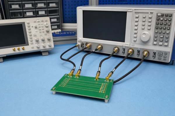
| TDR | Impedance versus propagation time | Locate and compare the via discontinuity |
| VNA | S-parameters over frequency | Find loss notches, reflections, and mode conversion |
| Eye or BER test | System margin at the receiver | Confirm link-level performance under the required setup |
For TDR, use a coupon or fixture with enough resolution and bandwidth to separate the via response from the launch. For VNA work, calibrate or de-embed to defined reference planes, preserve port polarity, and convert to mixed-mode parameters correctly for a differential structure. Compare the measured notch and time-domain discontinuity with the simulated result; a large mismatch often points to incorrect Dk, loss, geometry, port definition, or fixture removal.
Finally, apply the interface specification’s required eye, jitter, return-loss, or insertion-loss mask. Do not turn a generic 50-ohm target or a simulated eye opening into a manufacturing acceptance limit unless the product specification defines it.
FAQs About Via Stubs
Q1: What are vias in PCB used for?
A1: Vias connect copper features on different PCB layers. Signal vias carry nets between routing layers, while ground and power vias connect reference or supply structures. Only the unused extension beyond the intended transition is a stub.
Q2: What are PCB stubs?
A2: A PCB stub is an unterminated branch connected to a transmission path. It may be a trace branch or an unused section of a plated via. Both can reflect energy, but their geometry and mitigation methods differ.
Q3: Do vias increase PCB cost?
A3: Standard through vias usually do not add a separate specialty-process charge. Cost can increase when the design requires blind or buried vias, sequential lamination, microvias, backdrilling, tighter depth control, extra coupons, or added inspection.
Q4: What do vias look like on a PCB?
A4: A visible via normally appears as a plated hole surrounded by an annular pad. Solder mask may cover it. The hidden barrel, internal pads, anti-pads, and any residual stub require stackup or cross-section information.
Q5: In the example below, would the GND via count as a stub because the top (red) copper is isolated?
A5: An isolated copper island does not automatically make the entire ground via a transmission-line stub. Determine whether current enters that branch, whether the island has a valid reference function, and whether the geometry creates a dangling resonant conductor. Remove purposeless copper, but do not classify every unused ground-via segment with the signal-via stub model.
Q6: Is there a reason why a via stub would be better than a via with a poor impedance match?
A6: Neither condition is inherently better across every frequency. A short stub can create a smaller broadband disturbance than a severely mismatched transition, while a longer stub can produce a narrow, deep resonance. Compare the complete S-parameter response across the required band instead of judging either geometry from one impedance value.
Q7: How do you judge the performance? By simulation or have you actually built the board already?
A7: Use simulation before fabrication and correlated measurements after fabrication. Build a stackup-specific field and channel model, then compare it with coupon geometry, TDR or VNA data, and the applicable link test. Measured hardware checks whether the material, fabrication, launch, and fixture assumptions were accurate.
Q8: Do you think that return vias would still be needed or useless when routing from a surface layer to the second internal layer sharing the same reference plane between those layers?
A8: A return via may be unnecessary when return current remains on one continuous reference plane. The decision still depends on the actual field transition, plane openings, connector geometry, and nearby stitching. Verify the return path rather than applying a universal rule based only on layer numbers.
Q9: When needing to route differential signals with two sets of vias, are there significant signal integrity benefits from controlled depth routing in comparison with routing from top to bottom?
A9: Controlled-depth routing helps when it moves the residual-barrel disturbance outside the useful channel band. Compare that benefit with pair asymmetry, spacing, return-via placement, polarity-reversal geometry, and fabrication tolerance. A shorter stub does not compensate for an unbalanced differential transition.
Q10: How much do you account for potential defective vias in manufacturing?
A10: Treat via reliability separately from signal-integrity optimization. Define annular ring, aspect ratio, plating, registration, inspection, coupon, and electrical-test requirements for the product class and stackup. Do not add redundant vias blindly; use documented fabrication controls and test evidence to manage the actual failure risk.
Conclusion
Control a via stub by specifying its connected layer pair, maximum residual barrel, and electrical acceptance limit. Estimate the first resonance and compare it with the channel requirement. When the estimate approaches the operating band, model the actual pad, anti-pad, return-via, and stackup geometry.
Before releasing the layout, place the maximum residual length and inspection expectation in the fabrication documentation. Correlate a representative structure with TDR or S-parameters when the interface margin demands it. For a stackup and backdrill DFM review, email sales@bestpcbs.com. Include the Gerber or ODB++ files, drill files, layer connection table, impedance targets, material requirement, and target channel specification.