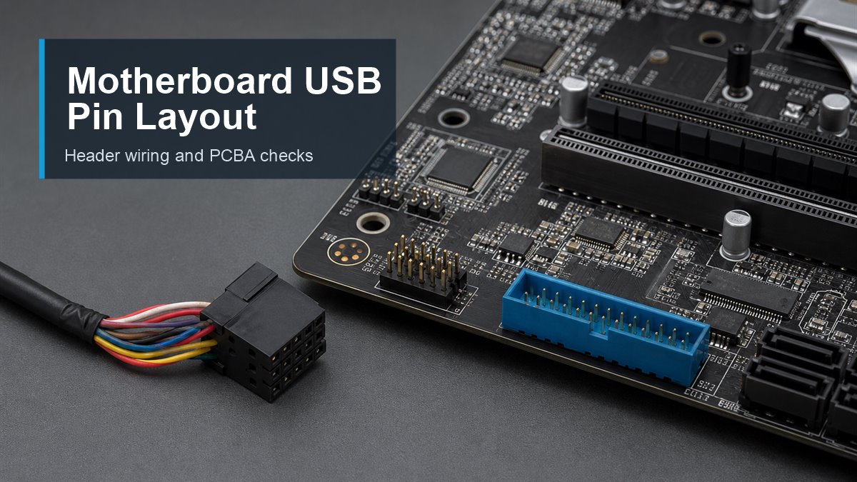
motherboard usb pin layout is the pin arrangement used by internal motherboard USB headers to carry +5V power, USB data signals, ground, key orientation, shield or drain connections, and sometimes over-current or USB-C sideband signals. For engineers, buyers, and PCBA teams, the pin layout is not only a computer assembly detail. It affects connector selection, PCB footprint accuracy, cable matching, assembly direction, inspection, and final functional testing.
A wrong USB header connection can cause a front-panel port that does not enumerate, a reversed cable, damaged pins, poor grounding, unstable data transfer, or in worse cases a short between power and signal pins. EBest Circuit (Best Technology) supports PCB manufacturing, PCB layout manufacturability review, component sourcing, PCBA assembly, and testing support for projects that use internal USB headers, USB connectors, wire harnesses, and front-panel I/O boards. If you need engineering support for a USB-related PCB or PCBA project, contact sales@bestpcbs.com.
What Is a Motherboard USB Pin Layout?
A motherboard USB pin layout shows how each pin on an internal USB header is assigned. These pins may provide power, differential data signals, ground, cable orientation, shielding, over-current detection, or other control functions depending on the header type.
On a finished computer motherboard, the layout is usually referenced by the board manual. In a custom PCB or PCBA project, the same idea appears in the schematic, PCB footprint, assembly drawing, cable drawing, and test procedure. The important point is that the connector, PCB footprint, wire harness, and enclosure direction must all match the same pin definition.
Some people search for this topic as usb pin layout motherboard, usb motherboard pin layout, USB header pinout, or usb mainboard pinout. The wording changes, but the engineering question is the same: which pin carries which signal, and how do we prevent the cable from being connected in the wrong direction?
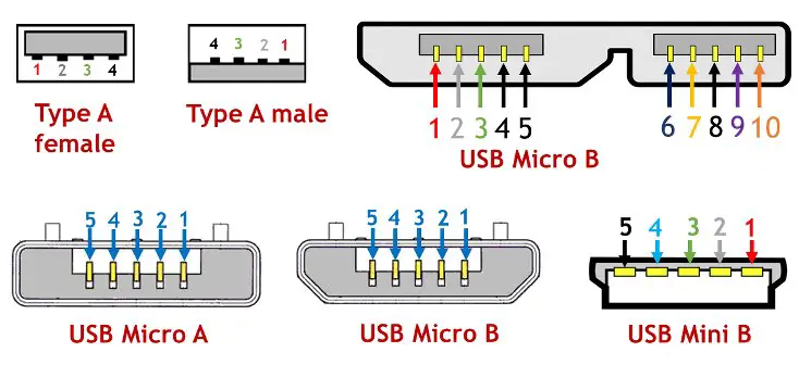
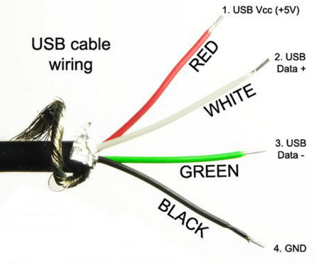
If you need a broader explanation of USB connector signal names and wire colors, this guide on USB pinout color code can be used together with this motherboard header guide.
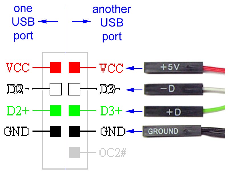
Motherboard USB 2.0 Header Pin Layout: VCC, D-, D+, GND, and Key
A common internal USB 2.0 motherboard header uses a 2×5 position layout with one blocked or missing pin. This missing pin is the key that helps prevent the cable from being installed in the wrong orientation. In many designs, the header supports two USB 2.0 ports from one connector.
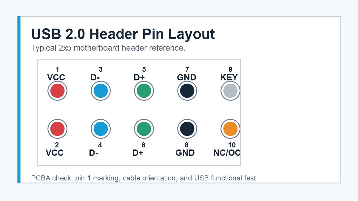
Typical USB 2.0 motherboard header reference:
| Pin area | Common signal | Function |
|---|---|---|
| VCC / +5V | USB power | Supplies 5V to the USB port |
| D- | USB data negative | Differential data line |
| D+ | USB data positive | Differential data line |
| GND | Ground | Return path and reference |
| Key / NC | Missing pin or no connection | Orientation control |
On many 9-pin USB 2.0 headers, one row serves one USB port and the other row serves the second USB port. However, designers should not assume every board uses the same extra pin definition. Pin 10 may be missing, no connection, shield, or over-current related depending on the motherboard or custom design.
For PCBA work, this is where small mistakes become expensive. If the silkscreen does not clearly mark pin 1, if the cable connector is not keyed, or if the assembly drawing only says “USB header” without the pin direction, the production team may need to stop and confirm the layout before assembly. That delay is much cheaper than repairing boards after the wrong cable has been installed.
USB 3.0 and USB 3.2 Gen 1 Header Pinout on a Motherboard
USB 3.0 internal headers are more complex than USB 2.0 headers because they carry both USB 2.0 signals and SuperSpeed differential pairs. In many motherboard documents, USB 3.0, USB 3.1 Gen 1, and USB 3.2 Gen 1 are used around the same 5Gbps generation, but the project documentation should follow the exact naming used by the connector supplier and customer specification.
A typical motherboard USB 3.0 header includes:
| Signal group | What it does | PCB/PCBA concern |
|---|---|---|
| VBUS / +5V | Provides USB power | Current rating and protection |
| USB2 D- / D+ | Supports USB 2.0 communication | Pair routing and correct polarity |
| SuperSpeed TX/RX pairs | Supports high-speed data | Differential pair impedance and length control |
| GND / drain | Ground and shield reference | Return path and EMI control |
| Key / orientation | Prevents wrong insertion | Connector direction and keepout |
The main risk is not only whether the pins are named correctly. The high-speed pairs must be routed as controlled differential signals, the connector footprint must match the chosen part, and the board must leave enough mechanical clearance for the thick front-panel cable. A design may look correct in the schematic but still fail in production if the connector exits toward a wall, heat sink, screw post, or enclosure rib.
For general connector pin definitions and diagrams, this related article on USB pinout diagrams may help when comparing USB-A, USB-B, Micro USB, USB-C, and internal header signal names.
USB Type-E Header Pin Layout for Front-Panel USB-C
A USB Type-E header is commonly used for front-panel USB-C connections. It is smaller and more compact than the traditional 19-pin USB 3.0 internal header, and it is designed for a different cable connector. From a PCB and PCBA point of view, the most important issue is compatibility: the motherboard header, front-panel USB-C cable, enclosure, and expected USB speed must match.
For custom projects, do not treat a Type-E header as a simple replacement for a USB 3.0 header. The connector footprint, insertion direction, mating height, retention force, signal definition, and current requirement may all change. If the design also involves USB-C current negotiation, product-level charging behavior, or special host/device behavior, the customer schematic and system design team should define those requirements clearly before PCB manufacturing.
EBest Circuit can review whether the PCB footprint, connector part number, assembly direction, BOM description, and manufacturability notes are consistent. We do not replace the customer’s system-level USB architecture or firmware decisions, but we can help reduce layout, assembly, and production risks before the board is built.
How to Identify USB Header Pins on a Motherboard?
The safest way to identify USB header pins on a motherboard is to start with the official board manual, schematic, or customer-controlled drawing. If the board is already in hand, the silkscreen mark, missing key pin, connector shape, and cable plug can help confirm the direction, but they should not replace the official pin definition.
Key checks include:
- Find pin 1 on the PCB silkscreen, drawing, or connector datasheet.
- Confirm whether the header is USB 2.0, USB 3.0 / USB 3.2 Gen 1, or Type-E.
- Check whether the cable is keyed, blocked, or made from separate single-pin wires.
- Match VCC, D-, D+, GND, shield, and over-current pins before powering the board.
- Confirm whether the front-panel cable exits in the correct mechanical direction.
- Record the final pin definition in the assembly drawing, not only in engineer notes.
The last point is important for repeat orders. A technician may assemble one sample correctly after a discussion with the engineer, but mass production needs a controlled drawing. Clear documentation prevents the same USB header question from being reopened every time the board is repeated.
Common Motherboard USB Header Wiring Mistakes
Motherboard USB header wiring mistakes often happen when a design uses a standard-looking connector but the cable, enclosure, or pin definition is not standard. A USB 2.0 front-panel cable may be separated into individual wires. A service-port cable may be handmade for prototypes. A custom industrial enclosure may rotate the board and make the cable approach from an unexpected direction.
Common failure points include:
- VCC connected to the wrong pin, creating a power risk.
- D+ and D- swapped, causing the USB device not to enumerate.
- Ground missing or connected through a weak return path.
- Pin 1 mark hidden after assembly.
- Key pin ignored when using loose wires instead of a keyed plug.
- USB 2.0 and USB 3.0 headers confused during cable selection.
- Type-E cable chosen without confirming motherboard support.
- Front-panel cable forced into the connector and bending header pins.
The practical fix is to make the USB connection unambiguous before assembly. The BOM should name the exact connector. The cable drawing should show wire order and mating direction. The PCB should mark pin 1 clearly. The PCBA instruction should define whether the cable is installed during assembly or tested separately after board production.
PCB Layout Checks for USB Header and Front-Panel Connector Designs
PCB layout checks for a USB header should cover both electrical and mechanical details. In production, the connector does not exist alone. It interacts with the cable, enclosure, screw positions, heat sources, nearby components, and the operator’s hand or fixture.
Important review points include:
- Footprint: Match the connector datasheet, pin pitch, hole size, pad size, and locating posts.
- Pin 1 marking: Keep pin 1 visible after assembly and cable insertion.
- Cable direction: Leave room for cable bend radius and locking tabs.
- Differential pairs: Route D+/D- and SuperSpeed pairs with correct polarity and impedance rules.
- Return path: Keep a clean ground reference near USB signals.
- ESD protection: Place protection devices close to external or user-accessible connectors.
- Keepout: Avoid tall components, screw bosses, shields, and enclosure walls near the cable path.
- Test access: Add accessible points or functional test steps where practical.
For USB 2.0, the routing is usually less demanding than SuperSpeed USB, but it still needs clean pair routing and correct polarity. For USB 3.0 or Type-E, the layout review becomes more sensitive because the high-speed pairs can be affected by impedance discontinuity, stubs, poor return path, and connector breakout routing.
This is also where a PCB supplier with DFM experience can help. A design may pass basic schematic review but still create assembly risk if the connector is hard to solder, difficult to inspect, or placed in a direction that the cable cannot realistically use.
PCBA Assembly and Testing Checks for Motherboard USB Headers
During PCBA assembly, motherboard USB headers should be checked as mechanical parts and electrical interfaces. Through-hole headers need correct insertion depth and vertical alignment. SMT USB connectors need controlled solder paste volume, reflow profile suitability, and enough pad strength for repeated cable insertion.
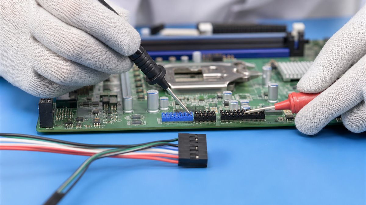
EBest Circuit checks USB header projects from several practical angles:
| PCBA stage | What should be checked | Why it matters |
|---|---|---|
| Incoming material | Connector model and cable match | Avoid wrong mating parts |
| SMT / THT assembly | Solder joints and alignment | Prevent weak joints and tilted headers |
| Visual inspection | Pin damage and orientation | Catch assembly mistakes early |
| Electrical check | Power, ground, and continuity | Reduce short/open risk |
| Functional test | USB device detection or data test | Confirm real port behavior |
For buyers, the key question is not only “Can you assemble this connector?” A better question is: “Can you help confirm the connector, cable, layout, assembly process, and test method before production?” That is the difference between placing a part on a board and delivering a usable PCBA.
EBest Circuit provides one-stop PCB manufacturing, component sourcing, PCBA assembly, DFM review, and testing support. Our team can help engineers review manufacturability risks before prototype, small-batch, or production orders.
Project Example: Preventing a USB Header Pin Layout Mismatch Before PCBA
A European industrial control customer needed a small batch of 80 PCBAs for an embedded controller. The board used an internal USB 2.0 header for a touch module and a service/debug port. The schematic showed VCC, D-, D+, and GND correctly, but the BOM only described the part as “2×5 USB header.” The cable drawing came from another supplier, and the enclosure required the cable to exit toward the left side of the board.
Project requirements:
- Quantity: 80 PCBAs for pilot production.
- Application: Industrial control panel with internal USB touch and service port.
- Connector: 2×5 USB 2.0 header with one keyed position.
- Assembly need: Cable must be easy to insert after the board is mounted in the enclosure.
- Delivery concern: Avoid rework because the customer had a fixed validation schedule.
Main challenges:
- The PCB silkscreen pin 1 mark was too close to the connector body.
- The cable drawing did not clearly show the mating direction.
- Pin 10 was not defined consistently between the customer note and connector reference.
- The cable exit direction was close to an enclosure wall.
- Functional testing needed to confirm both power and USB data behavior.
EBest Circuit solution:
- Reviewed the connector datasheet, PCB footprint, BOM, and cable drawing together.
- Asked the customer to confirm the final pin 10 requirement before purchasing parts.
- Suggested a clearer pin 1 mark and assembly note for cable insertion direction.
- Checked the keepout area around the connector for cable bend space.
- Added a test step to confirm USB device detection after assembly.
Result:
The customer corrected the drawing before PCBA production. The first pilot batch avoided reversed cable installation, USB non-enumeration, and enclosure interference. For the buyer, the value was not only a clean solder joint. The real value was catching a layout and documentation mismatch before it became a production problem.
FAQs About Motherboard USB Pin Layout
What is the standard motherboard USB pin layout?
A common USB 2.0 motherboard header uses VCC, D-, D+, GND, and a key or no-pin position. USB 3.0 and Type-E headers use more pins because they support additional high-speed signals. Always confirm the exact board manual or project drawing before connection.
Is motherboard USB pin layout the same as USB pinout?
They are related, but not exactly the same. USB pinout can describe many USB connectors, such as USB-A, Micro USB, or USB-C. Motherboard USB pin layout usually refers to internal headers used to connect front-panel or internal USB cables.
Can a USB 2.0 cable connect to a USB 3.0 motherboard header?
Not directly in most cases. USB 2.0 and USB 3.0 internal headers use different connector structures and pin arrangements. Some adapter cables exist, but the project should confirm compatibility, current rating, mechanical fit, and expected USB function.
Why does a USB header have a missing pin?
The missing pin is usually used as a key to prevent incorrect cable orientation. It helps the plug fit only one way when the connector and cable are properly matched.
How can EBest Circuit help with motherboard USB header PCB or PCBA projects?
EBest Circuit can support PCB manufacturing, DFM review, PCB layout manufacturability review, component sourcing, PCBA assembly, and functional testing support. For USB header projects, we can help check connector footprint, pin 1 marking, cable direction, soldering risk, and test requirements. Send your files to sales@bestpcbs.com for review.
In Conclusion, motherboard usb pin layout should be checked before PCB fabrication, cable sourcing, and PCBA assembly, not after the board fails to power or enumerate a USB device. A clear pin definition, correct connector footprint, visible pin 1 mark, practical cable direction, and functional test plan can prevent many avoidable USB header problems. EBest Circuit (Best Technology) helps engineers turn these details into manufacturable PCB and PCBA builds with DFM review, sourcing, assembly, and testing support.