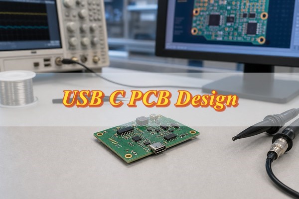
USB C PCB Design should start with a port specification, not a copied connector footprint. Define the data mode, power role, maximum negotiated power, and Alternate Mode requirements before selecting the connector, controller, protection network, and PCB stackup.
What Does a USB-C PCB Design Need to Support?
Define the port function before selecting the connector or starting layout. A USB-C receptacle can provide power only, USB 2.0 data, SuperSpeed data, USB Power Delivery, an Alternate Mode, or a combination of these functions. The connector shape does not guarantee a protocol, speed, or power level.
Start with a one-page port specification. State whether the product is a power source, power sink, or dual-role device; whether it needs USB 2.0, USB 3.x, USB4, or no data; the maximum negotiated voltage and current; and whether DisplayPort or another sideband function is required. Then identify the controller, PHY, connector, cable assumptions, and compliance target that support that exact feature set.
| Required Function | Essential Circuit Blocks | Layout Consequence |
| Power sink only | CC terminations or sink controller, VBUS protection, power conversion | Prioritize safe VBUS copper, connector mechanics, and CC placement |
| USB 2.0 device | D+/D- PHY, CC configuration, ESD protection | Route one controlled differential pair with a continuous return path |
| SuperSpeed device | High-speed PHY, orientation switch or integrated mux, CC controller | Route multiple high-speed pairs with strict stackup and loss control |
| USB Power Delivery | PD controller, power-path FETs, sensing, protection, optional VCONN | Separate sensitive control routing from high-current switching paths |
| Alternate Mode | Mode-capable controller, mux, SBU and high-speed lane routing | Add lane switching, sideband protection, and interface-specific checks |
Do not specify “USB-C” as the only requirement. A fabrication and assembly team needs the exact connector part number, stackup, impedance requirement, assembly side, and inspection criteria. The electrical team also needs the selected controller reference design and datasheet constraints.
How Do You Choose and Place a USB-C PCB Connector?
Choose from the connector manufacturer’s current drawing. Match the connector to the required USB functions, enclosure geometry, finished PCB construction, and assembly process.
- Contact set: Use a 24-contact receptacle when SuperSpeed lanes or sideband functions are required. A reduced-pin connector is suitable only when its available VBUS, GND, D+/D-, and CC contacts match the intended power-only or USB 2.0 circuit.
- Electrical rating: Verify rated current, working voltage, contact resistance, mating-cycle rating, and any manufacturer derating. Do not infer capability from connector appearance.
- Mounting style: Select top-mount, mid-mount, or straddle-mount from the enclosure datum, finished PCB thickness, and permitted board-edge position.
- Footprint orientation: Compare the schematic symbol and land pattern with both the mating view and PCB view. Confirm A/B-side pin numbering, signal-pad pitch, shell tabs, locating features, paste apertures, and solder-mask clearances.
- Board-edge position: Align the mating face with the enclosure opening and preserve clearance for the plug shell and cable overmold through the complete insertion path.
- Mechanical retention: Use the specified through-hole stakes, SMT tabs, or hybrid anchors so insertion and extraction forces are carried by the shell supports rather than the signal pads.
- Assembly access: Reserve space for paste printing, optical inspection, solder-joint access, selective rework, enclosure fasteners, and any keep-out specified below or behind the connector.
- Placement order: Place the receptacle first, then arrange ESD protection, orientation switching, required AC-coupling components, and VBUS protection immediately behind it. Keep exposed paths short and avoid branches, long stubs, and unnecessary neck-downs.
Which USB-C Pins Does Your PCB Design Actually Need?
Connect only the pin groups required by the selected port function, but never omit the CC implementation. The 24-contact receptacle contains repeated VBUS and GND contacts, duplicated USB 2.0 contacts for reversible insertion, two sets of SuperSpeed lanes, CC1/CC2, and SBU1/SBU2.
| Pin Group | Purpose | Design Decision |
| VBUS and GND | Power delivery and return | Connect all required contacts with balanced, low-resistance copper |
| D+ and D- | USB 2.0 data | Join the duplicated receptacle contacts as the connector documentation directs, while minimizing stubs |
| TX/RX pairs | SuperSpeed data | Route through the approved orientation mux or PHY topology |
| CC1 and CC2 | Attach, orientation, role, current advertisement, PD communication | Use the correct Rp, Rd, or Type-C/PD controller architecture |
| SBU1 and SBU2 | Sideband signals for supported modes | Leave unused only when the selected implementation permits it |
| Shield | Connector shell and high-frequency interference path | Implement the chassis or PCB grounding strategy defined for the product |
For a USB 2.0-only receptacle, the SuperSpeed and SBU contacts may remain unused when the connector and controller documentation allow it. For a full-featured port, both plug orientations must reach the correct PHY lanes through the selected mux or integrated controller. If you need a broader comparison of USB connector families, review the pin configuration of USB port before returning to the Type-C-specific design decisions here. Avoid naming nets only by pin number; functional names make schematic review and test-point planning clearer.
How Should USB-C PCB Traces Be Routed for USB 2.0 and SuperSpeed?
Route USB 2.0 D+/D- and SuperSpeed TX/RX as separate controlled-impedance systems. Use the production stackup and the selected PHY’s channel limits rather than copied trace dimensions.
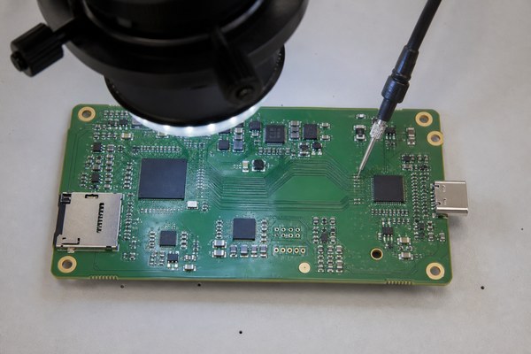
- Set the impedance: State the required differential impedance in the fabrication drawing and identify every controlled pair. Let the PCB fabricator calculate line width and spacing from the finished copper, dielectric thickness, material, solder mask, and reference-plane distance.
- Keep pairs coupled: Route each positive and negative conductor together with consistent width, spacing, and layer assignment. Avoid unnecessary separation around pads or components.
- Preserve the reference: Keep every pair over a continuous plane. Do not cross plane splits, voids, antipad fields, or poorly stitched layer transitions.
- Limit discontinuities: Minimize long neck-downs, test pads, branches, connector-to-protection stubs, and abrupt geometry changes.
- Control pair skew: Follow the PHY vendor’s intra-pair skew limit. Add tuning only where the added bends do not create excessive coupling or impedance variation.
- Manage vias: Use the fewest practical layer transitions, keep both signal vias geometrically balanced, reduce unused via stubs where required, and place ground-return vias beside the transition.
- Separate noise sources: Keep data pairs away from switch-node copper, inductors, oscillators, clocks, and other fast-edge or high-current nets.
- Verify lane mapping: Confirm mux connections, plug-orientation routing, polarity inversion, and lane swapping against the controller documentation. Do not assume the PHY supports every swap.
- Check the full channel: Include connector breakout, protection devices, muxes, vias, and package escape in the loss and discontinuity review; a short PCB trace alone does not prove compliance.
How Do CC1 and CC2 Work in a USB-C PCB Design?
CC1 and CC2 make the receptacle reversible. When a plug is inserted, only the CC contact connected through the cable detects the partner. The controller uses that active contact to determine plug orientation and select the corresponding SuperSpeed lane path.
A sink presents Rd on both CC pins. A source presents Rp on both CC pins and reads the detected CC voltage to confirm attachment and advertise the available Type-C current. A dual-role port needs a Type-C or PD controller to alternate and manage the source and sink states; fixed resistors alone cannot implement controlled role changes.
After attachment, the active CC line remains the configuration path and carries USB PD signaling when PD is supported. The other CC contact can supply VCONN to an electronically marked or active cable. CC1 and CC2 must remain separate; shorting them together prevents correct orientation detection and VCONN control.
On the PCB, place the CC terminations, controller, and protection close to the connector, keep both CC routes short, and protect them against ESD and possible VBUS overvoltage. During bring-up, test both plug orientations and verify the CC states, VBUS enable timing, advertised current, and PD negotiation. A source must keep VBUS off until a valid sink attachment is detected.
How Should USB-C Power Delivery Be Designed on a PCB?
Design every VBUS component and copper segment for the highest permitted PD contract and its credible fault conditions. Do not qualify the path only at the 5 V startup state.
- Set the power target: Define source, sink, or dual-role operation; maximum negotiated voltage and current; required PD revision; cable current capability; and whether Standard or Extended Power Range applies.
- Rate every component: Check the connector, protection IC, power-path FETs, current-sense element, capacitors, converter, and discharge circuit against the maximum contract voltage, continuous current, and credible transients.
- Size the VBUS path: Calculate resistance and voltage drop through contacts, copper planes, neck-downs, vias, switches, and the sense element. Connect parallel VBUS contacts into balanced copper so one contact does not carry a disproportionate share.
- Control power sequencing: Follow the controller reference design for attach detection, FET turn-on, soft-start, inrush limiting, VBUS discharge, reverse-current blocking, and detach behavior.
- Route current sensing: Use Kelvin connections where required, keep the sense pair symmetrical, and separate it from switch nodes and gate-drive currents.
- Provide VCONN correctly: Add the specified current-limited and protected VCONN path when the port must power an electronically marked or active cable.
- Manage heat: Calculate FET and sense-resistor dissipation at continuous load, provide copper area and thermal vias, and verify temperature rise inside the final enclosure at the highest ambient condition.
- Protect fault paths: Include overcurrent, short-circuit, overvoltage, reverse-voltage, and VBUS-to-CC/SBU fault protection appropriate to the port role and maximum voltage.
- Validate the implementation: Test every supported contract with qualified cables and partners while recording VBUS ripple, voltage drop, inrush, current limit, discharge time, component temperature, and PD messages. Claim only power levels supported by the complete hardware, firmware, cable, and compliance result.
Where Should USB-C ESD and Overvoltage Protection Be Placed?
Place protection immediately behind the receptacle, before connector-exposed traces reach the controller or power path. Keep the discharge route short and low-inductance.
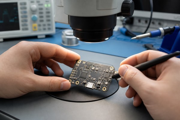
- Establish the protection boundary: Place each device between the receptacle and the protected controller or power circuit. Do not position sensitive components on the connector side of that boundary.
- Protect high-speed lanes: Select low-capacitance ESD devices whose bandwidth, insertion loss, package, and flow-through pinout fit the USB 2.0 or SuperSpeed channel budget.
- Protect CC and SBU: Match the normal working voltage and supported mode, then add short-to-VBUS overvoltage protection where connector faults can expose these pins to VBUS. A low-voltage ESD diode alone may not survive that fault.
- Protect VBUS: Choose overvoltage, surge, reverse-current, and current-limit protection for the maximum supported PD voltage and the port’s source or sink role.
- Use flow-through routing: Route connector pins into the protection device and then onward to the controller. Avoid branches, long stubs, unnecessary test pads, and repeated neck-downs.
- Shorten the ground return: Connect protection ground pads to a solid low-inductance ground structure with short copper and nearby vias. Do not route a discharge through a long thin trace before reaching the plane.
- Separate exposed traces: Keep the short connector-side segment away from protected signals, clocks, reset lines, and high-impedance nodes to reduce ESD coupling.
- Verify device limits: Check working voltage, clamp voltage, dynamic resistance, capacitance, pulse rating, leakage, package parasitics, and the system-level ESD target for each signal group.
- Inspect and test the path: Review connector-to-device placement in the PCB layout, confirm assembly polarity and grounding, then perform controlled ESD and fault testing on the assembled product rather than relying on component ratings alone.
How Do USB-C PCB Stackup, Impedance, and Board Thickness Work Together?
Finished board thickness is a mechanical requirement. Select it from the USB-C connector drawing, mounting style, enclosure datum, and manufacturing tolerance. A top-mount receptacle may work with several standard thicknesses, while a mid-mount or straddle-mount part can impose a narrow thickness range. A nominal 1.6 mm board is not a universal USB-C requirement.
Controlled impedance comes from the production stackup, not the overall board thickness alone. Trace width, pair spacing, finished copper thickness, dielectric thickness and dielectric constant, solder mask, and distance to the reference plane all affect the differential impedance. The target must come from the applicable interface and PHY requirements; the final geometry should be calculated for the fabricator’s actual materials and process.
The layer arrangement must give each USB pair a continuous reference plane from the connector to the PHY or mux. USB 2.0 can often be implemented on a well-planned four-layer board, but SuperSpeed routing may justify more layers when the design needs cleaner reference planes, shorter fanout transitions, less coupling to switching power, or additional routing space. Adding layers helps only when the resulting stackup improves the signal and return paths.
Before fabrication, provide the connector drawing, finished thickness and tolerance, copper weights, material family, proposed layer stack, differential-impedance targets, and the location of every controlled pair. Ask the PCB manufacturer to return the producible trace geometry for approval and to verify impedance with the agreed coupon or test method. That measurement confirms the fabricated transmission-line geometry; it does not by itself prove that the complete USB channel passes signal-integrity or compliance testing.
What USB-C PCB Design Mistakes Cause Charging or Data Failures?
Use the symptom to select the first circuit domain to inspect, not to declare a root cause. Each row below is a diagnostic starting point; confirm the fault with measurements, schematic review, layout review, and controlled substitution.
| Failure Symptom | Probable Failure Domain | Initial Diagnostic Check |
| VBUS remains absent after connection | CC termination, controller supply, port-role configuration, or power-path enable logic | With a known-good partner and cable, measure CC1, CC2, VBUS, controller supply, and power-switch gate timing during attachment |
| Port works in only one plug orientation | CC2 path, duplicated USB 2.0 contacts, orientation-mux control, or one SuperSpeed lane set | Repeat the same test in both orientations, then compare CC detection, mux state, and end-to-end connectivity for the affected lane set |
| USB 2.0 attachment occurs but enumeration fails | D+/D- connectivity, pair topology, protection-device loading, reference-path discontinuity, or solder defect | Inspect the connector joints, verify D+/D- pin mapping and stubs, and observe reset and enumeration signaling with the intended host |
| SuperSpeed falls back or disconnects | Channel loss, intra-pair skew, via discontinuities, plane gaps, mux configuration, or connector breakout | Confirm the negotiated link state, review the complete channel from receptacle to PHY, and run the applicable transmitter, receiver, or channel tests |
| USB PD contract is not completed | CC protection path, PD-controller configuration, firmware policy, cable capability, or VBUS switching sequence | Capture PD protocol messages while recording CC, VBUS, current, and power-switch gate timing |
| Connector, FET, or sense element overheats | Contact resistance, unbalanced VBUS current sharing, copper neck-down, insufficient vias, or component conduction loss | Measure millivolt drop across each path segment and component temperature at the maximum supported continuous load |
| Damage follows insertion or an ESD event | Protection working voltage, clamp path, short-to-VBUS exposure, or high-inductance discharge return | Verify component ratings and connector-to-protection placement before repeating controlled fault or immunity testing |
Record the partner, cable capability, plug orientation, negotiated mode, load, temperature, and measurement points for every failure. A certified cable is useful for isolation, but it does not certify the end product or increase the port’s implemented capabilities.
What Should You Check Before Sending a USB-C PCB to Fabrication?
Run a joint schematic, layout, mechanical, manufacturing, and test review before releasing Gerber or ODB++ data. A final design-rule check does not prove that the port role, footprint, stackup, or protection strategy is correct.
- Freeze the port specification: Record the USB data mode and maximum data rate, power role, maximum voltage and current, PD behavior, Alternate Modes, and cable assumptions.
- Verify the connector: Compare the symbol, pin numbering, footprint, 3D position, shell stakes, and board thickness with the connector manufacturer’s current drawing.
- Audit CC behavior: Check CC1 and CC2 components, dead-battery behavior, controller supply, VCONN, and source/sink state transitions.
- Review every signal path: Trace D+/D-, TX/RX, SBU, polarity, mux control, AC coupling, vias, and reference planes end to end.
- Confirm the stackup: Obtain the fabricator’s proposed dielectric and copper construction and approve the controlled-impedance geometry.
- Calculate the power path: Check copper width, planes, neck-downs, via count, contact sharing, voltage drop, and component dissipation.
- Inspect protection placement: Confirm connector-first routing, low-inductance returns, suitable capacitance, and overvoltage ratings.
- Check assembly access: Review paste apertures, thermal mass, connector coplanarity, inspection visibility, rework space, and panel orientation.
- Add useful test points: Expose controller rails, VBUS, CC nodes, fault outputs, and low-speed controls without creating high-speed stubs.
- Release complete data: Provide fabrication notes, impedance table, Gerber or ODB++, drill files, BOM, pick-and-place data, assembly drawings, and test requirements.
For a production-oriented USB C PCB Design review, include the controller and connector datasheets with the release package. They let the fabricator and assembler distinguish intentional features from missing data and flag footprint or stackup conflicts before boards are built.
FAQs About USB-C PCB Design
Q1: Can a USB-C receptacle be replaced with a similar-looking part?
A1: Treat every connector substitution as a footprint and qualification change. Compare contact population, pin numbering, mounting height, board-edge datum, shell stakes, rated current, mating life, paste pattern, and keep-outs before approving the alternate part.
Q2: How should USB-C connector solder joints be inspected?
A2: Use inspection methods that cover both visible anchors and hidden signal joints. Combine optical inspection with X-ray or another validated method when the connector body obscures critical pads, then add mechanical and functional checks appropriate to the product.
Q3: Can a USB-C receptacle be hand-soldered on a prototype?
A3: Hand soldering is acceptable only when every joint can be formed and inspected without damaging the connector or PCB. Fine hidden contacts and large shell tabs often make controlled reflow or hot-air assembly more repeatable.
Q4: Which cable should be used to validate a USB-C board?
A4: Use known-good cables whose certified data rate and power capability match each tested mode. One charge-only, USB 2.0, or lower-rated cable cannot validate unsupported SuperSpeed or high-power behavior.
Q5: Does using a certified USB-C cable make the product compliant?
A5: No, cable certification does not certify the end product. It reduces one test variable, while the port, protocol, power behavior, signal integrity, interoperability, and product implementation still require their applicable verification.
Q6: What should a production USB-C functional fixture test?
A6: Test the functions that can reveal assembly escapes without duplicating full compliance testing. Typical coverage includes both orientations, VBUS presence and drop, CC detection, USB enumeration, negotiated mode, selected PD contracts, and connector continuity.
Q7: When should a damaged USB-C connector be replaced instead of reworked?
A7: Replace it when contacts, insulator, shell retention, plating, or PCB pads are mechanically compromised. Cosmetic shell marks may be reviewable, but intermittent contact, lifted pads, deformation, or heat damage should not be accepted through repeated touch-up.
Q8: What surface finish is suitable for a USB-C connector footprint?
A8: Select the finish with the connector footprint and assembly process. ENIG is common for fine-pitch SMT boards, but solderability, flatness, shelf life, cost, and the assembler’s validated process should drive the final choice.
Q9: Should the USB-C shell connect directly to digital ground?
A9: The shell connection must follow the product’s EMC and chassis-ground strategy. Enclosure construction, cable shielding, ESD return paths, safety requirements, and verification results determine whether the connection is direct or uses a controlled coupling network.
Q10: What connector records should be controlled for production?
A10: Control the manufacturer, exact part number, revision, approved alternates, drawing, qualification evidence, and incoming-inspection criteria. This prevents an unreviewed mechanical or electrical change from entering assembly under a generic BOM description.
Conclusion
Do not release a USB-C PCB until the port role, connector footprint, CC behavior, VBUS rating, controlled-impedance stackup, protection boundary, and both plug orientations have been verified. Freeze those decisions before ordering prototypes, then use measured bring-up results to correct the design before production tooling or volume assembly.
Send your Gerber or ODB++ files, BOM, quantity, connector drawing, stackup, impedance requirements, assembly needs, firmware or programming scope, and test plan to sales@bestpcbs.com. EBest Circuit can review the manufacturing package for PCB fabrication, controlled impedance, connector assembly, inspection access, and production-test requirements before the build.