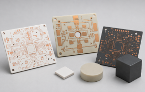
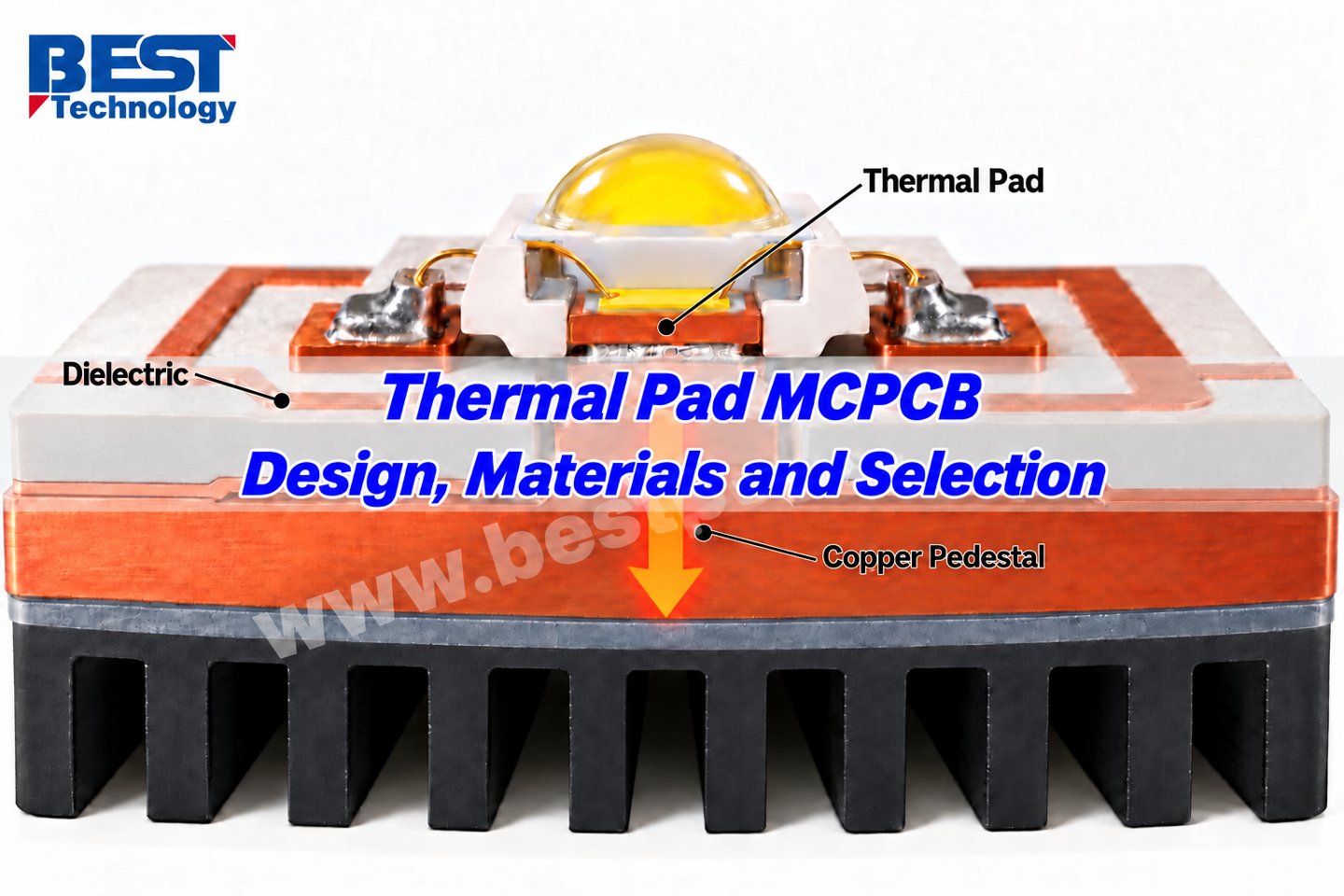
A thermal pad MCPCB commonly refers to a metal-core board that connects an LED’s thermal pad to a metal pedestal through a solder joint, bypassing the dielectric beneath that pad. This direct thermal path can reduce one part of the heat-flow resistance. It works only when the package’s electrical connections and the board’s isolation scheme allow that connection.
The first design decision is therefore electrical as well as thermal: can the LED’s heat-transfer pad safely connect to the metal base? Once that is established, compare the complete path through the package, solder, board, mounting interface and heat sink.
Key Takeaways
- A direct thermal path bypasses dielectric locally beneath the LED thermal pad; other circuitry still needs insulation.
- A copper base alone does not prove that a board has a direct thermal path.
- Dielectric thickness, conductivity and effective heat-transfer area must be considered together.
- A board-to-heat-sink interface pad serves a different purpose from a solderable thermal land.
- Verify package compatibility, solder quality and operating temperature before approving a stack-up.
What Does “Thermal Pad MCPCB” Mean?
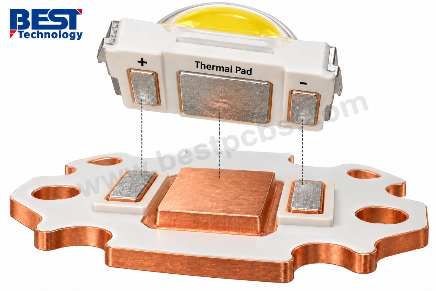
In LED board discussions, the term often describes a direct-thermal-path MCPCB rather than a soft pad placed under a circuit board. A metal pedestal reaches the LED’s thermal contact location, with a soldered connection between the package and pedestal.
PCB thermal pads can refer to different parts. Three related parts are easy to confuse:
- Package thermal pad: the exposed heat-transfer surface on the underside of the LED or component.
- Board thermal land: the solderable surface that mates with that package pad.
- Thermal interface pad: a separate material between the board base and heat sink.
For a thermal pad PCB, specify which one you mean on drawings and quotation requests. Asking for a “thermal pad” without a cross-section can result in a different construction from the one intended.
How Does a Direct Thermal Path Differ from a Conventional MCPCB?
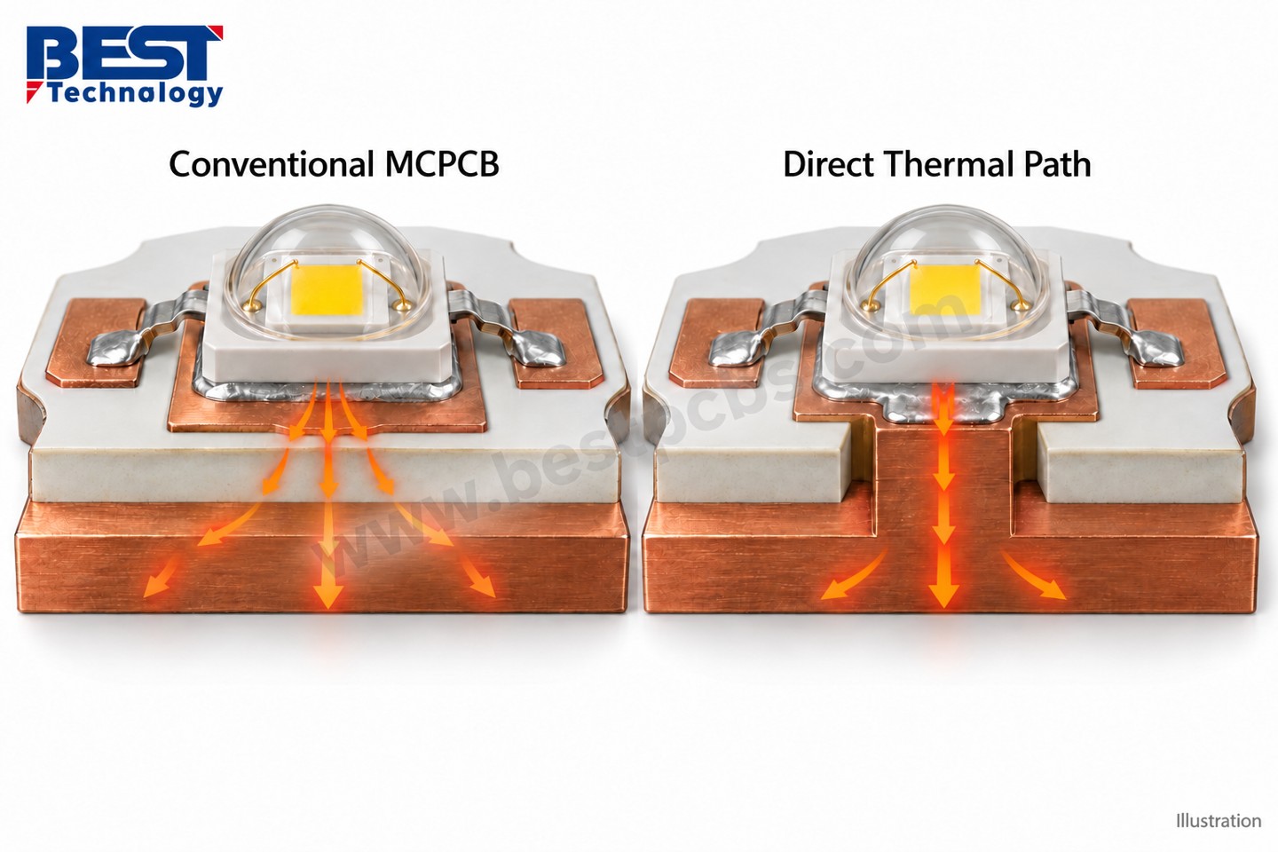
A conventional insulated MCPCB carries heat through its dielectric before it reaches the metal base. A direct thermal path bypasses that dielectric at the designated thermal contact while retaining electrical insulation beneath the surrounding circuit.
Cree LED describes heat flowing from the LED package through its thermal pad into the PCB and onward to a heat sink. Adura’s SinkPAD description explains the local dielectric bypass and specifies compatibility with electrically neutral thermal pads. Neither principle makes every LED package interchangeable.
At EBest Circuit, we provide metal-core PCB manufacturing and PCB assembly services. For a thermal-pad design, send the LED part number and proposed stack-up together so we can review the board and assembly requirements against the same package information.
Which Material Parameters Should You Compare?
Compare dielectric thickness and dielectric thermal conductivity on the same basis before comparing material grades. A conductivity value for a metal base or a complete test structure cannot simply replace the dielectric value.
The following published Henkel/Bergquist examples describe Thermal Clad dielectric grades. They are reference material data, not measured performance or confirmed stock for an EBest Circuit board.
| Dielectric Grade | Thickness (µm) | Dielectric k (W/m·K) |
| HT-04503 | 76 | 2.2 |
| HT-07006 | 152 | 2.2 |
| MP-06503 | 76 | 1.3 |
Source and conditions: Henkel/Bergquist’s Thermal Clad Comprehensive Selection Guide, dielectric selection table. Thickness uses an optical method; dielectric conductivity uses extended ASTM D5470. Values are published reference characteristics. The table does not provide a temperature-specific curve, so these numbers should not be treated as guaranteed across the operating range.
HT-04503 and HT-07006 illustrate why thickness matters: their listed dielectric conductivity is the same, but their thickness differs. MP-06503 provides a same-thickness comparison with HT-04503. Confirm the current grade, construction and applicable data sheet before ordering.
When Should You Choose a Conventional or Direct-Path Board?
Choose a conventional insulated MCPCB when its verified thermal performance and electrical isolation meet the design. Evaluate a direct-path structure when resistance beneath a compatible package pad is a significant part of the thermal budget.
| Selection Point | Conventional MCPCB | Direct Thermal Path |
| Below the thermal land | Dielectric separates land and base | Metal connection bypasses dielectric locally |
| Electrical relationship | Land remains isolated by the specified dielectric | Thermal contact connects electrically to the base |
| Package suitability | Depends on isolation and heat budget | Requires a compatible pad connection and geometry |
| Primary selection trigger | Specified isolation and temperature target are met | Local dielectric resistance needs reduction |
| Heat-sink interface | Still needs a suitable mounting interface | Still needs a suitable mounting interface |
A direct-path board does not remove the package’s internal thermal resistance or the heat sink’s limits. If the dominant problem is a poor mounting interface or inadequate cooling to ambient, changing the board alone may deliver little improvement. Compare alternatives with the same LED, heat load, mounting arrangement and ambient conditions.
How Can You Estimate Dielectric Thermal Resistance?
For a uniform layer carrying heat straight through its thickness, estimate MCPCB thermal resistance with R = t / (k × A). Use thickness t in metres, conductivity k in W/m·K and area A in m²; the result is K/W.
Calculated example, not a test result: assume a 100 µm dielectric, conductivity of 2 W/m·K and a uniform 5 × 5 mm heat-transfer area.
- t = 0.0001 m
- A = 0.005 × 0.005 = 0.000025 m²
- R = 0.0001 ÷ (2 × 0.000025) = 2 K/W
- At an assumed 3 W of heat crossing that layer, ΔT = 3 × 2 = 6 K.
This simplified calculation excludes lateral spreading, solder and mounting contact resistance, package resistance, temperature-dependent properties and parallel heat paths. It is useful for comparing variables, not predicting an assembled LED’s junction temperature. Use heat dissipated into the path, rather than automatically treating all electrical input as heat.
How Should You Define the Thermal Pad and Electrical Isolation?
PCB thermal pad design starts with the exact component’s recommended land pattern and pad connection. There is no universal MCPCB thermal-pad size that fits every LED with the same external package dimensions.
- Identify the pad’s electrical function. Confirm whether it is neutral, connected to an electrical terminal, or subject to a specified connection requirement.
- Match the footprint. Check the thermal contact, anode, cathode, orientation and clearances against the current package drawing.
- Define the cross-section. Show where dielectric remains and where the thermal contact joins the metal base.
- Review the enclosure connection. Decide whether the base is floating, grounded or connected mechanically to conductive parts.
- Approve assembly geometry. Confirm pedestal height, coplanarity and solder-joint requirements with the board and assembly teams.
Do not connect an electrically active thermal pad to a common metal base merely because the footprint fits. An unexpected base connection can change the circuit or create a short. Package documentation and the approved isolation design take priority over a generic board drawing.
Does a Direct-Path MCPCB Still Need Thermal Interface Material?
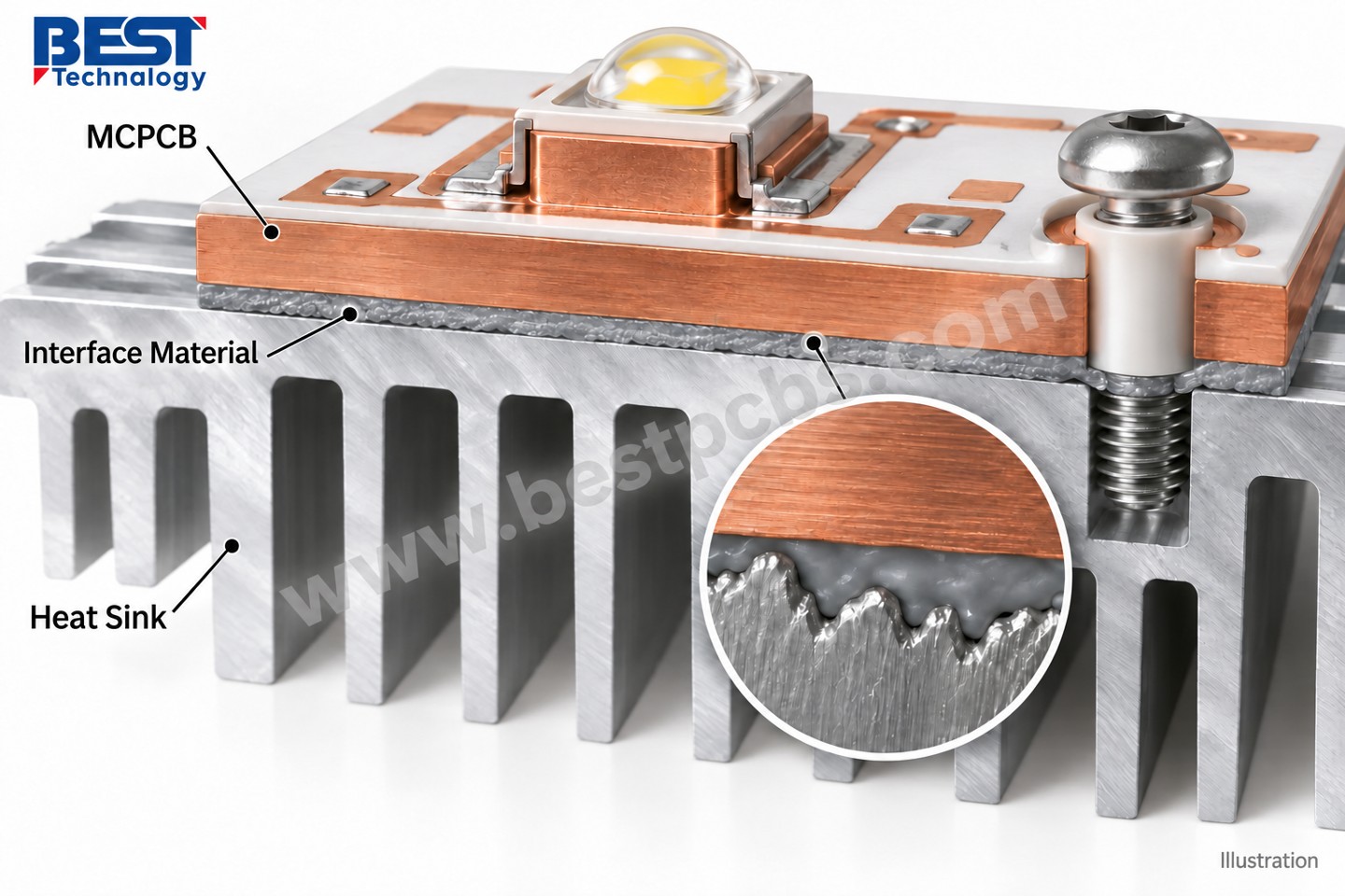
It may still need interface material between the metal base and heat sink because a direct path inside the board does not eliminate the separate mounting interface.
Choose an interface for the actual gap, surface flatness, clamping arrangement and electrical isolation requirement. A compliant pad may accommodate a gap that a thin grease layer cannot; adding unnecessary thickness can also increase resistance. Use the interface supplier’s pressure and thickness data for the selected product.
Do not insert a soft gap pad into a location designed for a soldered LED thermal contact. Those materials perform different jobs and require different assembly conditions.
How Do You Verify the Assembled Thermal Path?
Verify electrical isolation and operating temperature in the final mounting arrangement; a successful continuity test alone does not establish thermal performance.
- Before assembly: compare the approved stack-up, package drawing, thermal contact location and circuit isolation.
- During assembly validation: confirm paste deposition, placement and a reflow profile suitable for the component and board. Use supplier guidance rather than a universal temperature setting.
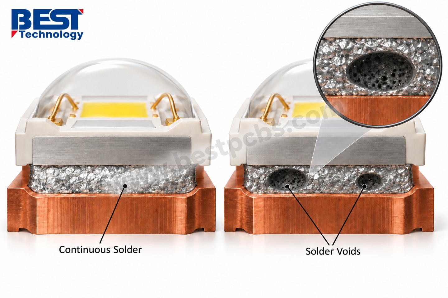
- After reflow: inspect hidden solder contacts with an appropriate method. Define voiding criteria for the actual package and application; do not adopt an unsupported universal percentage.
- During operation: record ambient conditions, drive current, mounting pressure or torque, interface material and measurement location. Run until temperatures stabilize.
- Before release: compare measured values and any junction-temperature estimate with the component’s specified limits and the project’s approved margin.
Stop the test if temperature exceeds the approved limit, rises abnormally, or electrical isolation fails. Review the suspected cause, make a controlled correction and repeat the same test conditions. An infrared image can locate a hot region, but it does not by itself prove the junction temperature or the cause of overheating.
What Should You Send Us for a Thermal Pad MCPCB Review?
Send the LED part number, manufacturing files and mounting details so we can assess the intended heat path and board requirements together.
- Gerber files, board outline and a proposed cross-section.
- LED data sheet, land pattern and thermal-pad electrical connection.
- Base material, dielectric grade and thickness, copper weight and surface finish.
- Heat load or operating conditions, temperature target and heat-sink interface.
- Quantity, assembly scope and required electrical and thermal checks.
For related construction options, see our direct-thermal-path board page. Email the project files to sales@bestpcbs.com. We will review the requested structure; material availability, pad geometry and acceptance requirements need confirmation for the actual design.