pcb
Home > Blog

Posts Tagged ‘surface treatment’

How to Distinguish Hard Gold and Soft Gold Plating on PCB?
星期五, 14 6 月, 2024

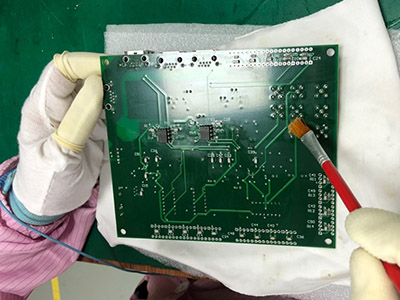
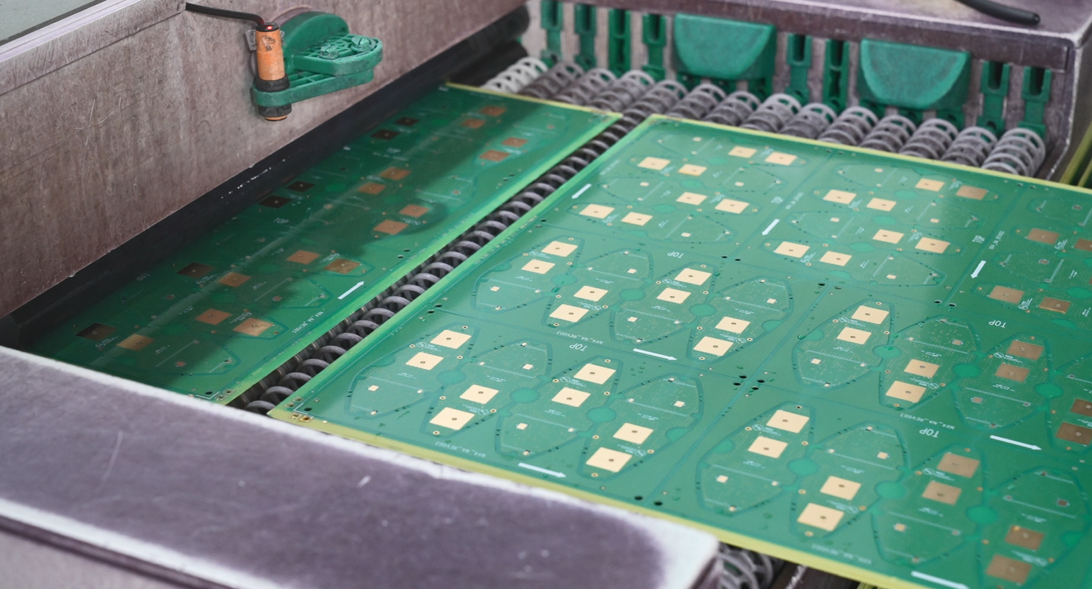
Gold plating is a common surface finish in PCB manufacturing, also known as nickel gold electroplating. It provides excellent conductivity, corrosion resistance and good durability to electronic devices. However, not all gold plating is created equal. There are two primary types of gold plating are used in PCB fabricating: hard gold plating and soft gold plating. They differ in properties, manufacturing process and applications, let’s explore it today!

How to Distinguish Hard Gold and Soft Gold Plating on PCB?

What are Hard Gold Plating and Soft Gold Plating?

In the manufacturing process of printed circuit boards (PCBs), we often hear the words “soft gold” and “hard gold”. They are actually describing the different metal materials used in the gold-plating process.

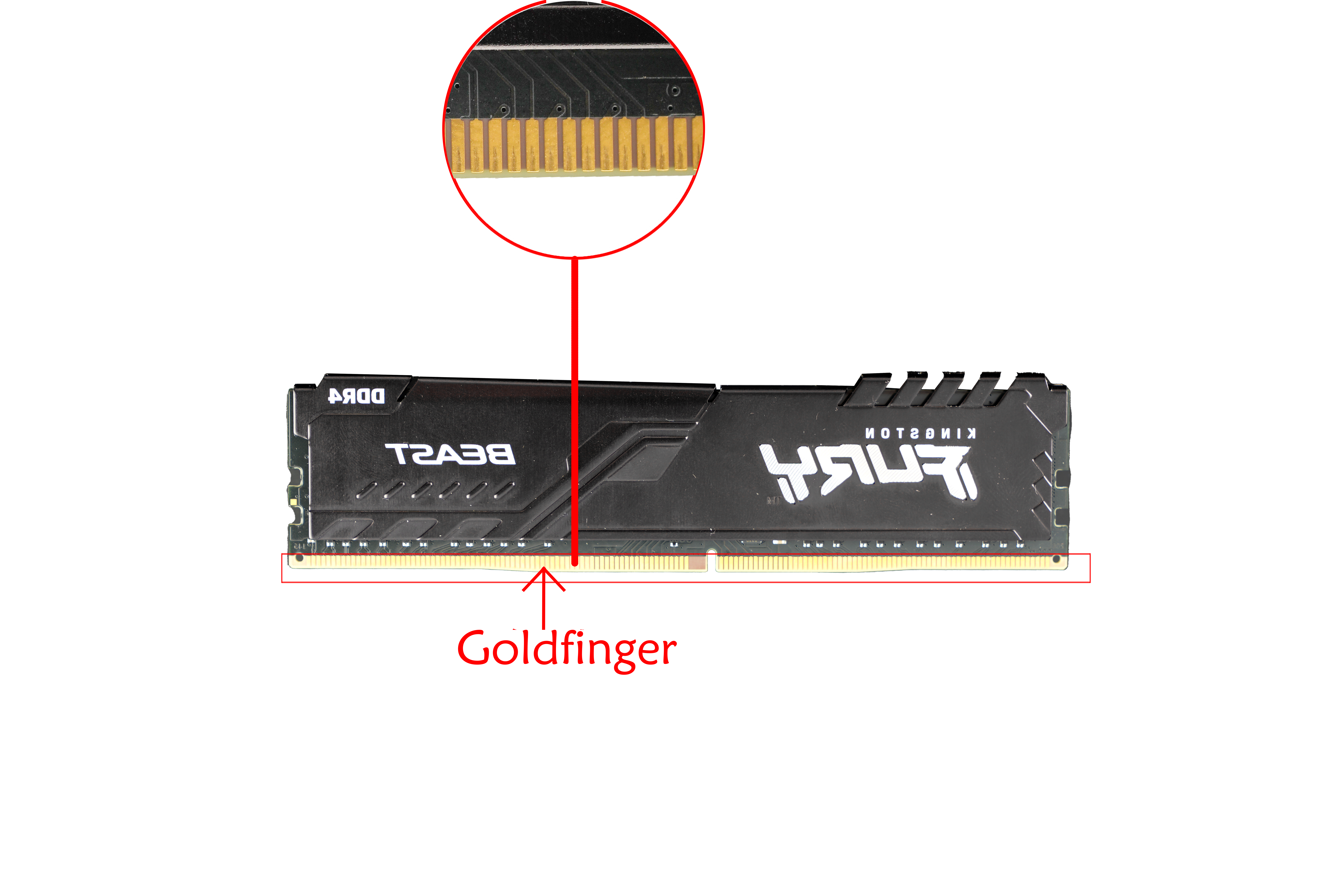
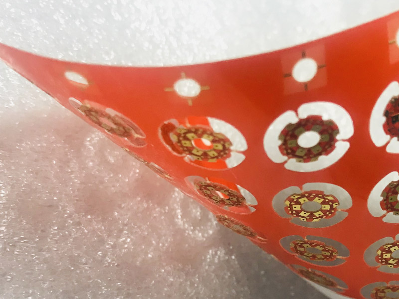
Hard gold usually refers to an alloy formed by electroplating process. This alloy is doped with other metal elements, such as nickel, cobalt, etc., to make it harder and more resistant to friction. Hard gold is especially suitable for places that require force and friction, such as the edge contact points of circuit boards (commonly known as “gold fingers”), because it can withstand frequent insertion and removal operations. Although the processing process of hard gold is complex, it can be doped with other metals to improve the hardness of gold, making it more suitable for making hollow jewelry or for industrial applications.

How to Distinguish Hard Gold and Soft Gold Plating on PCB?

Soft gold refers to the state of pure gold or close to pure gold, because of the high purity of gold, it is relatively soft. Soft gold is mainly used for aluminum wire on COB (Chip On Board), or the contact surface of mobile phone keys, because it can maintain good electrical conductivity and weldability. The processing process of soft gold is relatively simple, does not require complex alloying process, and maintains the soft characteristics of gold, which is suitable for the production of solid jewelry or for applications requiring good electrical conductivity.

How to Distinguish Hard Gold and Soft Gold Plating on PCB?

Properties and applications: hard gold plating vs soft gold plating

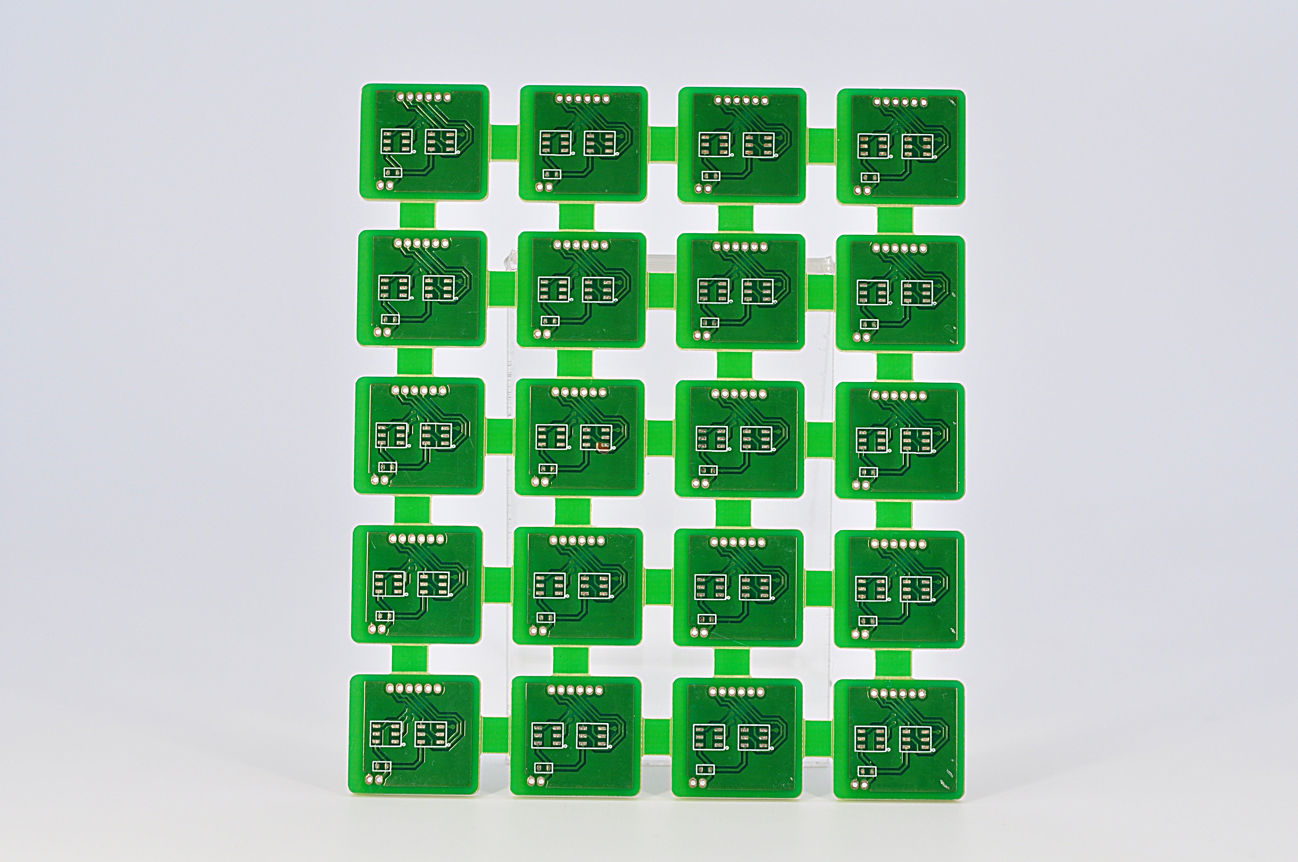
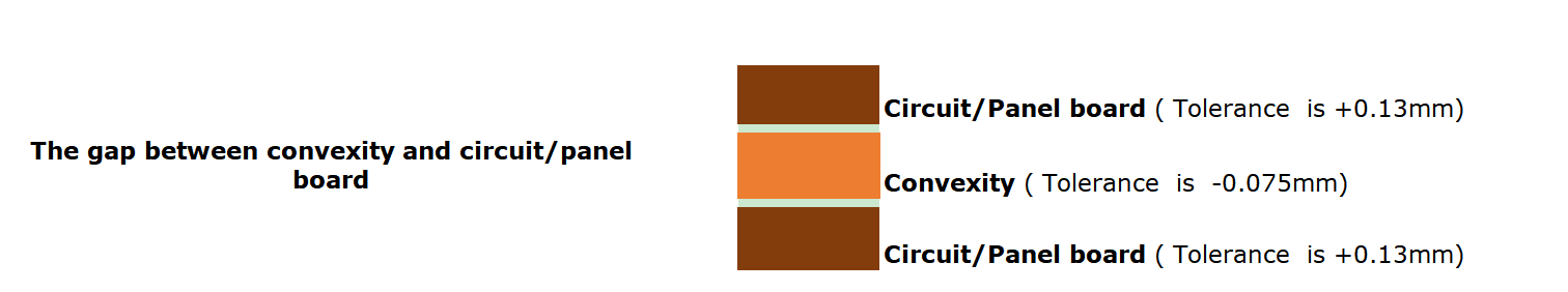
Hard gold plating is known for its high hardness, typically achieved by alloying gold with small amounts of nickel or cobalt. So, it has highly resistant to wear and mechanical stress. The thickness of hard gold plating is usually greater than that of soft gold plating, ranging from 30 to 50u’’ or more. Best Technology can make up to 50u’’ if you required. Due to the hardness of the hard gold plating, they are commonly used in edge connectors, keypads, and contact points where repeated mechanical action occurs.

The manufacturing process of soft gold plating involves a chemical process to deposit a thinner layer of pure gold onto the PCB surface. The coated pure gold without any alloying elements, resulting in a softer finished compared to the hard gold plating. Additionally, the thickness of soft gold plating is typically thinner than that of hard gold plating, usually around 1 to 3u’’. Due to the softness and conductivity properties, the soft gold plating technology is often used in applications requiring high conductivity and precision, such as wire bonding and fine-pitch components in high-frequency and high-speed circuits.

What’s the difference between gold plating and immersion gold?

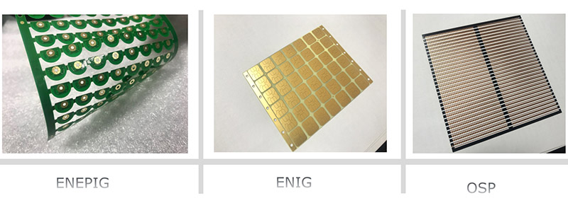
Actually, Immersion Gold is mostly called ENIG (electroless nickel immersion gold) surface treatment method. The advantage of this method is that nickel and gold can be attached to copper without electroplating process, and its surface is smoother than gold plating, which is especially important for the shrinking electronic parts and components requiring flatness.

The method of leaching gold is chemical deposition. A coating is formed by chemical redox reaction, which is generally thick. Electroplating gold is based on the principle of electrolysis, also known as electroplating. Most other metal surface treatments are electroplating. In actual product applications, 90% of the gold PCB board is dipped in gold, because the poor weldability of the electric gold-plated board is its fatal defect.

How to Distinguish Hard Gold and Soft Gold Plating on PCB?

Nickel gold coating with stable color, good brightness, smooth coating and good weldability can be deposited on the surface of printed circuit by gold leaching process. It can be divided into four stages: pretreatment (degreasing, micro-etching, activation, post-leaching), nickel plating, gold leaching, post-treatment (waste gold washing, DI washing, drying). The thickness of gold leaching is 0.025-0.1um. Gold is used in the surface treatment of the circuit board because gold has strong electrical conductivity, good oxidation resistance and long service life. General applications such as keyboard board, gold finger board, etc.

Choosing between hard gold plating and soft gold plating for your PCB depends on your specific application requirements. At Best Technology, we offer expert guidance and high-quality PCB manufacturing services to help you select the best surface finish for your needs. Choose us as your trusted PCB supplier to ensure reliable and efficient solutions for all your electronic projects.

You may also like

What Are Differences of ENIG VS ENEPIG in PCB Manufacturing – Series 2
星期二, 2 1 月, 2024

In our last blog, we simply introduced ENIG surface treatment in PCB manufacturing, and this time, we will share more information about the comparison of ENIG and ENEPIG.

What is ENEPIG Surface Treatment?

ENEPIG stands for Electroless Nickel Electroless Palladium Immersion Gold. This type of metal coating on the PCB pad surface consists of three layers—nickel, palladium, and gold. Apart from protecting the copper surface from corrosion and oxidation, the ENEPIG surface treatment is also suitable for high-density SMT (Surface Mount Technology) designs.

For its manufacturing process, manufacturers begin by activating the copper surface, followed by depositing a layer of electroless nickel, then a layer of electroless palladium, and finally, a layer of immersion gold. The process is somewhat similar to the one they follow in the ENIG process, but adding a palladium layer to the ENIG technology. The palladium layer not only improves the surface protection of the PCB, but also prevents nickel from deteriorating and inhibits interactions with the gold layer.

Pros of ENEPIG Surface Treatment

  • Reduce the black pad issues
  • Excellent solderability and high reflow soldering performance
  • Provide high-reliable wire bonding capability
  • High-density design available
  • Meet the miniaturization standards
  • Suitable for extra thin PCBs

Cons of ENEPIG Surface Treatment

  • Expensive than ENIG process
  • Thicker palladium layer will decrease the effective of SMT soldering
  • Longer wettability time

What are the Differences Between ENIG and ENEPIG?

The main difference between ENIG and ENEPIG is the palladium layer. This is the extra layer that added in ENEPIG process, which provides high oxidation resistance, enhance the electrical performance of the surface cleanliness and improve the abrasion resistance of the PCB surface. However, the palladium layer also increases the cost of manufacturing.

Additionally, the inconsistent surface cleanliness of ENIG, resulting from low solder joint reliability, particularly in gold wire bonding, is a concern. Extra procedures are also required to prevent nickel corrosion in ENIG. When considering it into manufacturing, the ENIG is well-suited for lower-end electronic products.

(ENIG_VS_ENEPIG)

The Considerations of Selecting ENIG or ENEPIG Surface Finishing

Though both two surface treatments offer excellent electrical performance and heat dissipation properties, there are still some conditions that need to consider when choose them.

  • Budget

Cost is an important factor when choose a suitable surface treatment. As we explain above, ENEPIG is expensive than ENIG, if you are trying to find a relative cost-effective coating, then ENIG is the best choice.

  • End-applications

The end-applications or finished products also determined the selection of surface finishing. For example, if your PCB will be used in high temperature applications, ENIG would be the better one since it can withstand high temperature.

  • Flatness

Many traditional surface finishes have poor flatness and smoothness, this brings the big challenge of small-size components mounted. Especially for those fine-pitch components like BGA, an uneven surface can result many problems. However, both ENIG and ENEPIG offer highly smooth surface finishes, forming thin and uniform layers on the solder pads.

  • Bonding demand

ENEPIG provides the optimal choice for wire bonding due to its highly smooth surface finish, which enhances wire bonding capabilities.

  • Environment-friendly

Some traditional surface treatments contain hazardous substances, making them non-compliant with RoHS requirements. Both ENIG and ENEPIG made by Best Technology are fully RoHS compliant and lead-free, so you are don’t worry about the environment unfriendly.

At the end, the choice between ENIG and ENEPIG surface treatments in PCB manufacturing involves a careful consideration of various factors. While both options offer excellent electrical performance, heat dissipation properties, and compliance with environmental standards like RoHS, specific project requirements and priorities will guide the decision-making process. If you are still confuse about the selection of surface treatment, welcome to contact with us, Best Team will give you a best solution that can meet your specific demands and save money for you.

You may also like

How to choose surface finish on Printed Circuit Board?
星期六, 17 12 月, 2022

When finish the PCB design, we should choose a suitable surface finish to protect traces from corrosion. Nowadays, the most popular surface treatments for PCB manufacturer to use are HASL/LF HASL, OSP and ENIG.

Different surface treatment has its unique functionality and the cost also is different. This article we will show you the pros and cons of the three surface finishing which use while the PCB manufacturing process.

HASL Surface Finish

HASL (Hot Air Solder Level) can be known as tin-lead HASL and lead-free HASL, it was the mainstream surface treatment technology in the 1980s, but with the increased of “small and high density” demands in PCB, there are less and less circuit boards use the HASL technology because it will cause the defective products due to the solder point are easy to leave on the board surface during SMT process. In view of this situation, some PCB board manufacturers or designers prefer use OSP or immersion gold to ensure the good quality products as well as smooth production process.

  • Tin-lead HASL

Advantages:

1) Economical and widely available.

2) Excellent solderability.

3)Better mechanical strength & lustrousness than lead-free HSAL.

Disadvantages: it is harmful to environment and violates RoHS compliance.

  • Lead-free HASL

Advantages: low cost, good solder performance and environmental.

Disadvantages: mechanical strength & lustrousness are not good than lead HASL.

In additional, due to the poor surface flatness of HASL circuit boards, neither leaded nor lead-free HASL is not suitable for soldering fine-pitch components or plated through-holes, because it will cause the short circuits and poor welding during the assembly process.

(LF_HASL)

OSP

OSP (Organic Solderability Preservatives) also named as pre flux, the working principle is to generate a layer of organic film chemically on the copper surface to protect the surface from oxidation or vulcanization in the room environment. Meanwhile, OSP also can increase the oxidation resistance, heat shock resistance and moisture resistance of a PCB. 

OSP is equivalent to an anti-oxidation treatment, the protective thin film can be easily removed by the flux quickly under the high soldering temperature, then it makes the exposed copper surface immediately combined with the molten solder in a very short time to become a solid solder spot.

At present, the usage of OSP surface finishing process has increased significantly because it is appropriated for both low and high-end products. If your application has no surface connection functional requirements or storage life limitations, the OSP process is the most desirable surface treatment process.

(OSP_surface_treatment)

Advantage:

1)With all the advantages of bare copper soldering, expired (more than 3 months) boards can also be resurfaced, but one time is better.

2)Good for fine-pitch, BGA and smaller components.

3)Low cost and easy to rework.

4)Simple process and easy to ensure quality.

Disadvantage:

1)OSP is easily affected by acid and humidity, so must be packed with vacuum.

2)Need to do surface treatment again if storage time more than 3 months.

3)It should be used within 24 hours after unpacking.

4)OSP is an insulating layer, so the test point must be printed with solder paste to remove the original OSP layer for electrical testing.

ENIG

ENIG (Electroless Nickel/Immersion Gold) is one of a chemical nickel gold deposition method, the working principle is to generate a layer of coating by chemical REDOX reaction to get a thicker gold layer. Currently, ENIG is mainly used in the surface of the circuit board with connection functional requirements and long storage life.

Advantage:

1)Can be stored long time as well as no oxidation.

2)Good flatness surface and suitable for small solder point components.

3)Good solderability.

4)Can be used as the base material for COB wire bonding.

Disadvantage:

1)High cost than other two surface treatments.

2)Easy to exist black-pad issue during production process.

(ENIG)

As we can know from above information, each PCB surface treatment has its own merit and demerit, you can choose the one according to the effect you want to reach, as well as your cost. 

If you don’t know which is best for you, you can send inquiry to us, our professional engineering team and PCB sales will choose the suitable one for you. Welcome to contact us if you have any other questions.

You may also like

Differences Between Immersion Gold and Gold Plating In PCB?
星期三, 7 12 月, 2022

With more and more extensive usage of Printed Circuit Boards, the IC become more and more integrated and IC pins on PCB are also more denser (such as 0603, 0402 spec ICs), which brings a big difficulty to SMT process. In addition, the shelf life of HASL board is very short, and Gold-plated board can solve such problems perfectly, that’s why it is common and popular to use gold board in high precision and ultra-small assembly process. Nowadays, there are two kinds of gold coating method in PCB industry – Immersion gold & Gold plating. To make you a sense of them, today we will simply introduce their definition and the differences between two of them.

Part 1: What is Immersion Gold (ENIG)

Immersion Gold also named as ENIG (Electroless Nickel/Immersion Gold) is generating a layer of coating by chemical REDOX reaction, is a kind of chemical nickel gold deposit surface finish during PCB manufacturing process. We can get a thicker layer of gold, but as its weak adhesion through immersion, it is also known as Soft Gold.

Part 2: What is Gold Plating

Gold plating is an another surface treatment of depositing a thin layer of gold on PCB surface by plating, the working principle is to dissolve nickel and gold (commonly known as “gold salt”) in the chemical potion, then immerse the circuit board in the electroplating cylinder and through the current on the copper foil surface of the PCB to generate a layer of gold plating. The gold particles attached to the PCB, as strong adhesion also known as “hard gold”. Gold plating is widely use in electronic products as its characteristics of hardness, excellent abrasion resistance and not easy to be oxidized. For example, the gold finger of flash driver in our computer is hard gold.

Part 3: The differences between Immersion Gold and Gold Plating

  • In generally, the gold thickness of immersion is thicker than plating, and immersion gold is golden yellow while gold plating is yellowish white, so just from appearance, most customers prefer like immersion gold.
  • Due to the crystal structures between them are different, immersion gold is easier to operate in SMT process, and won’t cause the poor soldering issue.
  • Immersion gold is softer than plating way, so if boards required gold fingers, it is always use plate-gold as its good wear resistance properties.
  • There is only nickel gold on the solder pad, so under the conductor skin effect, the signal transmission won’t be affected in copper layer.
  • Compared with gold plating, immersion gold has more denser crystal structure and is not easy to oxidation.
  • With the denser line width and space requirements, plating method is easily to cause short circuits, but since immersion gold board only has gold on solder pads, which won’t exist such issue.
  • The adhesive between solder mask and copper layer on circuit is stronger as there is only nickel gold on immersion board, so it is easier for engineers to make compensation when adjust line space.
  • Black-Pad won’t be happened to immersion board after assembly because it has good flatness than plating method.
  • Immersion gold is more economy than plating.

Best Technology is a professional PCB manufacturer with over 16 years experiences, and we have rich and mature technical to fabricate immersion gold and gold-plated boards. Warm welcome to contact us at sales@bestpcbs.com if you have any questions or RFQs about printed circuits, we are always online.

You may also like

Why ENEPIG More Suitable for Ceramic PCB Wire Bonding?
星期四, 20 10 月, 2022

There are many surface treatment choices that can be used on Ceramic PCB, but why ENEPIG is one of options we always recommend to our customers whom have wire bonding demands?

In the application of Ceramic PCB, COB or wire bonding was widely used for the packaging technology in thin, short, high speed of electronic products. The Chip On Board (COB) technology refers to a technology in which bare chips are directly attached to the PCB board and then connected electronically through metal wires, namely “Wire Bonding”. Due to gold wire has an excellent electrical conductivity, thermal conductivity, corrosion and oxidation resistance, gold wire is often used as a main bonding material in microelectronics packaging.

What is ENEPIG?

ENEPIG, is a type of surface treatment on Printed Circuit Boards and ceramic PCB, the full name of it is Electroless Nickel – Electroless Palladium – Immersion Gold, now it is widely used in wire bonding field.

How does it work and what’s the standard thickness of each layer?

  • Electroless Nickel: Nickel acts as a barrier layer, preventing copper from interacting with the other metals involved in this plating technology, particularly gold. The layer is deposited on the catalytic copper surface using an oxidation-reduction reaction. The result is a layer that is between 2.0 to 5.0 microns thick.
  • Electroless Palladium: Palladium is a relatively stable metal at room temperature, and it is difficult to be oxidized within 400℃. The chemically deposited palladium layer has a neat lattice arrangement, uniform grain size and compact structure. Adding palladium layer between nickel layer and gold layer can effectively prevent the diffusion of nickel layer to gold layer. The Palladium is a layer with a thickness between 0.03 to 0.10 microns, it also depends on the final applications.
  • Immersion Gold: The main function of the gold layer is to bond with the gold wire. If there is no palladium layer as a diffusion barrier between the nickel layer and the gold layer, the gold layer can also bond with the gold wire after reflow, as long as the gold layer reaches a certain thickness. For example, when the thickness of the electroplated nickel gold reaches 0.3um, it can bond with the gold wire. In addition, gold itself has a good bonding ability with gold wire, and in ENEPIG process, due to the palladium layer protects the gold layer from the pollution of nickel, only a thin gold layer (0.03um~0.05umm) is needed to have a good bonding property. This’s why there’s cost advantage of ENEPIG than that of thicker ENIG.
(ENEPIG product)

Why choose ENEPIG?

ENIPIG has a good wiring bonding ability, solder joint reliability, multiple reflow soldering and excellent storage time, can correspond to and meet the requirements of a variety of different assemblies.  Below is a comparison about performance of different surface treatments:

(Comparison-about-performance-of-different-surface-treatments)

Advantages  of ENEPIG

  • “Black Nickel” free — The palladium layer separates the Nickel layer from the gold layer, it can prevents the mutual migration of gold and nickel, so no black nickel will appear
  • Excellent gold wire bondability — the gold plating/coating is very thin, can be used for gold wire bonding as well aluminum wire bonding
  • Palladium acts as an additional barrier layer to further reduce copper diffusion to surface, thus ensuring good solderability
  • Cost-effective than ENIG
  • Lead-free nickel
  • Good compatibility between coating and solder paste
  • Very suitable for packaging components such as SSOP, TSOP, QFP, TQFP, PBGA

Best Technology is a 16+ years PCB manufacturer and we made many ENEPIG PCBs and ceramic PCBs for our customers, welcome to contact us if you have demands on ENEPIG PCB.

You may also like

What kind of finishing recommended for the extra thin FR4 PCB
星期四, 18 6 月, 2020

As we know, the extra thin PCB means the thickness of printed circuit board is more thin than normal PCB, which is refer to a thickness smaller than 0.4mm for 1L/ 2L & 4L PCB. For extra thin PCB, we know they are all very thin and are easily to be broken, so the option for the surface treatment of the extra thin PCB is very crucial.

So, what kind of finishing to be recommended for the extra thin Rigid PCB?

extra thin FR4 PCB
0.15mm extra thin FR4 PCB_Best Technology

Generally, there are 3 kinds finishing can be recommended for the extra thin PCB. It is OSP, ENIG (Electroless Nickel Immersion Gold), and ENEPIG.

extra thin pcb finishing

But you may want to ask that lead-free Tin is also a common finishing for the PCB. Why not recommend LF HASL? 

That’s because while LF HASL Process, the PCB will be easy to be blew away, people will use heated compressed air to leveling (blowing) on the coating molten tin (lead) solder, during this process, the traces will be easy to be broken as well.

So normally, we will not recommend the LF HASL finishing for an ultra thin FR4 PCB.

HASL lead-free is only suitable for a board with minimum thickness of 0.6mm, while the standard gold immersion surface coating can support PCB with a minimum thickness of 0.2mm. For the surface treatment of ENEPIG , which plate only needs to be about 0.1 microns for palladium and about 0.1 microns for gold, (palladium is a precious metal that is much harder than gold), so for board with ENEPIG finishing, its surface will looks more smooth, that’s also why it is the most recommended surface treatment for an extra thin PCB.

extra thin PCB
0.13mm extra thin Rigid FR4 PCB_Best Technology

If you are searching for an extra thin PCB, feel freely to ask or send your inquiry to us. We will be pleased to share you more information regarding the extra thin PCB.

You may also like