

There are many surface treatment choices that can be used on Ceramic PCB, but why ENEPIG is one of options we always recommend to our customers whom have wire bonding demands?
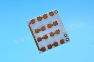
In the application of Ceramic PCB, COB or wire bonding was widely used for the packaging technology in thin, short, high speed of electronic products. The Chip On Board (COB) technology refers to a technology in which bare chips are directly attached to the PCB board and then connected electronically through metal wires, namely “Wire Bonding”. Due to gold wire has an excellent electrical conductivity, thermal conductivity, corrosion and oxidation resistance, gold wire is often used as a main bonding material in microelectronics packaging.
What is ENEPIG?
ENEPIG, is a type of surface treatment on Printed Circuit Boards and ceramic PCB, the full name of it is Electroless Nickel – Electroless Palladium – Immersion Gold, now it is widely used in wire bonding field.
How does it work and what’s the standard thickness of each layer?
- Electroless Nickel: Nickel acts as a barrier layer, preventing copper from interacting with the other metals involved in this plating technology, particularly gold. The layer is deposited on the catalytic copper surface using an oxidation-reduction reaction. The result is a layer that is between 2.0 to 5.0 microns thick.
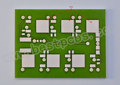
- Electroless Palladium: Palladium is a relatively stable metal at room temperature, and it is difficult to be oxidized within 400℃. The chemically deposited palladium layer has a neat lattice arrangement, uniform grain size and compact structure. Adding palladium layer between nickel layer and gold layer can effectively prevent the diffusion of nickel layer to gold layer. The Palladium is a layer with a thickness between 0.03 to 0.10 microns, it also depends on the final applications.
- Immersion Gold: The main function of the gold layer is to bond with the gold wire. If there is no palladium layer as a diffusion barrier between the nickel layer and the gold layer, the gold layer can also bond with the gold wire after reflow, as long as the gold layer reaches a certain thickness. For example, when the thickness of the electroplated nickel gold reaches 0.3um, it can bond with the gold wire. In addition, gold itself has a good bonding ability with gold wire, and in ENEPIG process, due to the palladium layer protects the gold layer from the pollution of nickel, only a thin gold layer (0.03um~0.05umm) is needed to have a good bonding property. This’s why there’s cost advantage of ENEPIG than that of thicker ENIG.
Why choose ENEPIG?
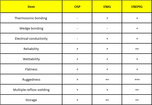
ENIPIG has a good wiring bonding ability, solder joint reliability, multiple reflow soldering and excellent storage time, can correspond to and meet the requirements of a variety of different assemblies. Below is a comparison about performance of different surface treatments:
Advantages of ENEPIG
- “Black Nickel” free — The palladium layer separates the Nickel layer from the gold layer, it can prevents the mutual migration of gold and nickel, so no black nickel will appear
- Excellent gold wire bondability — the gold plating/coating is very thin, can be used for gold wire bonding as well aluminum wire bonding
- Palladium acts as an additional barrier layer to further reduce copper diffusion to surface, thus ensuring good solderability
- Cost-effective than ENIG
- Lead-free nickel
- Good compatibility between coating and solder paste
- Very suitable for packaging components such as SSOP, TSOP, QFP, TQFP, PBGA
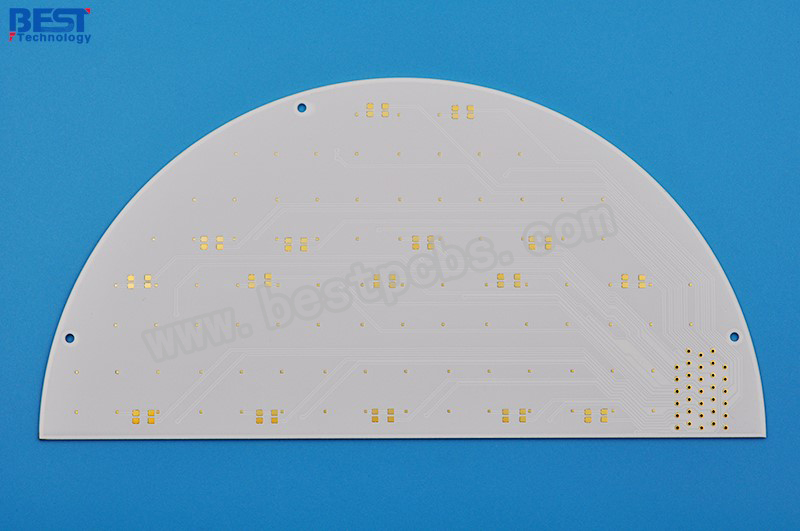
EBest Circuit (Best Technology) is a 16+ years PCB manufacturer and we made many ENEPIG PCBs and ceramic PCBs for our customers, welcome to contact us if you have demands on ENEPIG PCB.
You may also like


Tags: surface treatment