A solder mask bridge is the narrow solder mask area left between nearby PCB pads or solder mask openings. It separates exposed copper pads, controls solder flow, and helps reduce solder bridging during SMT assembly.
This feature matters most in fine-pitch PCB designs. If the bridge is wide enough, it supports stable soldering. If it is too narrow, it may break, shift, disappear, or become a solder mask sliver.
This guide explains solder mask bridge width, minimum design limits, solder mask aperture bridges, common defects, gang opening decisions, and PCB fabrication rules.
What Is a Solder Mask Bridge?
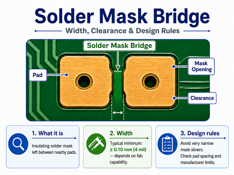
A solder mask bridge in PCB is the strip of solder mask material left between two adjacent solder mask openings. It is formed by the solder mask layer, not by copper.
Its role is to keep solderable pads separated during assembly. When molten solder spreads during reflow, the bridge works as a physical barrier and helps prevent solder from joining nearby pads.
This feature is common around fine-pitch ICs, connectors, QFN pads, QFP leads, small SMD parts, and dense test pad arrays. In these areas, pad spacing is tight, so the remaining mask area must be checked carefully.
A solder mask bridge is a solder control feature, not an electrical connection.
Why Does a PCB Need a Solder Mask Bridge?
A PCB uses a solder mask bridge to improve solder control and reduce short-circuit risk during assembly. This is especially important when exposed pads are close together.
Main functions include:
- Separating nearby solder pads during reflow.
- Reducing solder bridging on fine-pitch components.
- Controlling solder paste spread after heating.
- Improving visual inspection around dense pad areas.
- Supporting stable batch assembly for repeat production.
Without this bridge, solder may flow more easily between adjacent pads. This can create shorts, increase rework, and reduce assembly yield.
Solder Mask Bridge vs Web vs Dam: Are They the Same?
Yes. In most PCB fabrication discussions, solder mask bridge, solder mask web, and solder mask dam refer to the same narrow solder mask area between two adjacent openings.
The difference is mainly usage. Bridge describes the shape. Dam describes the function of blocking solder flow. Web describes the thin mask strip seen in DFM reports.
| Term | Meaning | Used In | Check Point |
|---|---|---|---|
| Solder Mask Bridge | Mask strip between pads | PCB layout | Finished width |
| Solder Mask Web | Thin mask strip | DFM review | Stability |
| Solder Mask Dam | Solder barrier | Fabrication | Minimum dam width |
| Solder Resist Dam | Same mask barrier | Supplier documents | Mask capability |
Solder Mask Bridge vs Opening: What Is the Difference?
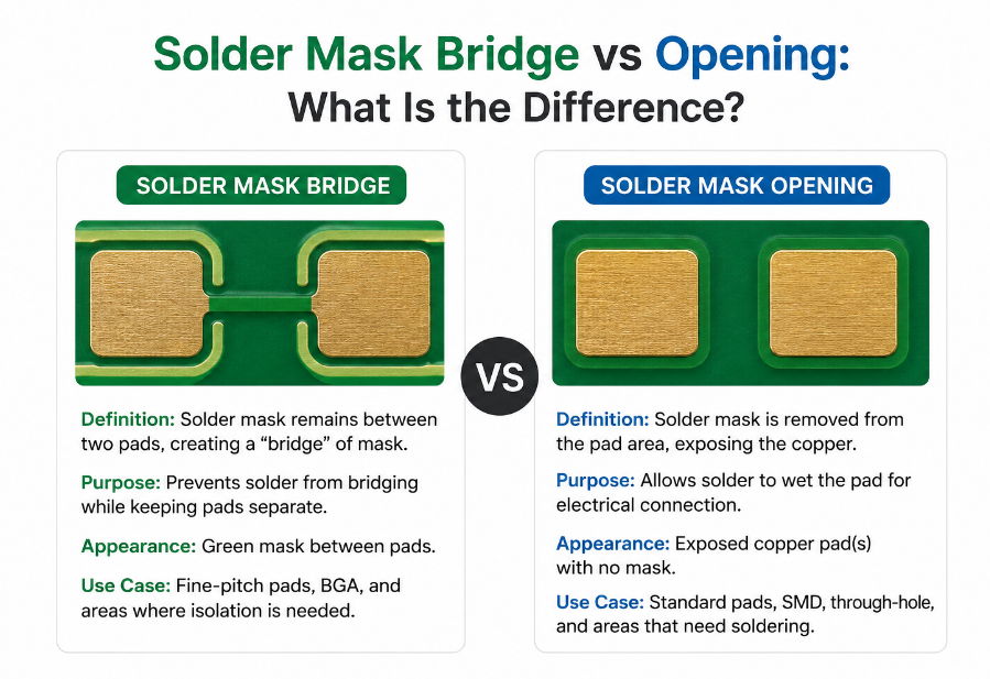
A solder mask bridge is the solder mask that remains between pads. A solder mask opening is the exposed area where solder mask is removed for soldering.
| Item | Solder Mask Bridge | Solder Mask Opening |
|---|---|---|
| Feature | Mask remains | Mask is removed |
| Location | Between pads | Over copper pad |
| Purpose | Blocks solder flow | Allows soldering |
| Controlled By | Dam width | Mask clearance |
| Risk | Broken or missing dam | Oversized opening |
| Assembly Effect | Reduces solder bridging | Supports solder wetting |
| Fabrication Concern | Width and adhesion | Pad exposure and alignment |
| Fix | Increase gap or use gang opening | Adjust clearance |
These two features must be checked together. If the solder mask opening is too large, the remaining bridge becomes smaller. If the opening is too small, solder mask may cover part of the pad.
How Is Solder Mask Bridge Width Calculated?
Solder mask bridge width is calculated from pad-to-pad spacing after solder mask clearance is applied on both sides.
Solder Mask Bridge Width = Pad-to-Pad Space − 2 × Solder Mask Clearance
For example, if two pads have 0.20 mm spacing and solder mask clearance is 0.05 mm per side, the remaining bridge width is:
0.20 − 0.05 × 2 = 0.10 mm
This calculation shows why copper spacing alone is not enough. The final mask bridge depends on the exposed opening size, not only the distance between copper pads.
Registration tolerance should also be considered. If the solder mask shifts during imaging, the effective bridge width may become smaller on one side.
What Is the Minimum Solder Mask Bridge Width?
The minimum solder mask bridge width depends on solder mask color, copper thickness, surface finish, imaging method, and factory capability. It is not one fixed value for all PCB suppliers.
| Condition | Common Reference | Note |
|---|---|---|
| Green solder mask | 4 mil / 0.10 mm | Easier for fine dams |
| Blue solder mask | 5 mil / 0.125 mm | Needs more margin |
| Red solder mask | 5 mil / 0.125 mm | Check fine-pitch pads |
| Black solder mask | 6 mil / 0.15 mm | Harder to expose and inspect |
| White solder mask | 7 mil / 0.175 mm | Wider dam preferred |
| Matte solder mask | 6–7 mil / 0.15–0.175 mm | Confirm first |
| Heavy copper PCB | Larger margin | Copper height affects mask edge |
| Fine-pitch IC | DFM review required | Do not rely only on CAD |
| Mass production PCB | More process margin | Repeatability matters |
Green solder mask usually supports narrower dams than black or white solder mask. Heavy copper, HASL finish, dense pad layout, and small registration margin can all require a wider bridge.
What Factors Affect Solder Mask Bridge Width?
Solder mask bridge width is affected by both PCB design and manufacturing control. A CAD file may show a bridge, but the finished board depends on real process limits.
Main factors include:
- Pad spacing: smaller pad gaps leave less solder mask between openings.
- Solder mask clearance: larger clearance reduces the remaining bridge.
- Mask registration: alignment shift can reduce effective bridge width.
- Solder mask color: green usually supports finer mask dams.
- Copper thickness: heavy copper makes mask edge control harder.
- Surface finish: ENIG is usually better for dense fine-pitch pads than HASL.
- Exposure control: weak exposure may reduce bridge strength.
- Developing pressure: strong developing may damage narrow mask features.
- Factory capability: each PCB supplier has its own safe production range.
These factors should be reviewed together. A bridge that is safe on a green standard copper PCB may not be safe on a black heavy copper PCB.
Solder Mask Bridge vs Sliver: What Is the Difference?
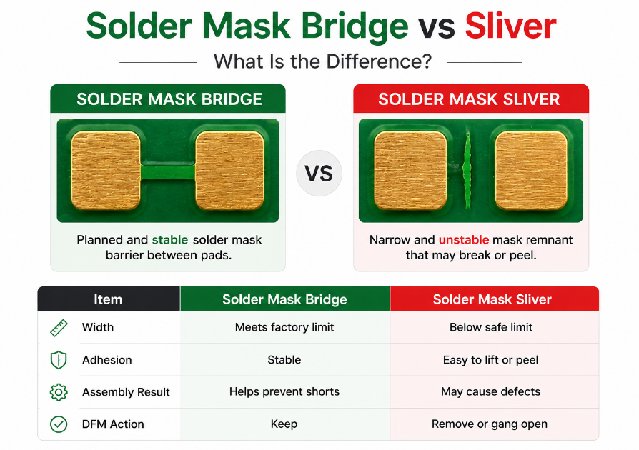
A solder mask bridge is a planned solder barrier. A solder mask sliver is a narrow, unstable mask remnant that may break, peel, or disappear.
| Item | Solder Mask Bridge | Solder Mask Sliver |
|---|---|---|
| Purpose | Planned barrier | Unstable leftover mask |
| Width | Meets factory limit | Below safe limit |
| Shape | Continuous | Thin or irregular |
| Adhesion | Stable | Easy to lift |
| Fabrication Result | Remains after processing | May break or disappear |
| Assembly Result | Helps prevent shorts | May create defects |
| DFM Action | Keep | Remove or gang open |
Slivers often appear when solder mask openings are too close or clearance is too large. In that case, the remaining solder mask cannot form a stable bridge.
What Are Common Solder Mask Bridge Defects and Causes?
- Missing dam:
The bridge is partly or fully gone. Main causes include small bridge width, excessive developing, oversized mask opening, or weak adhesion. Risk: solder bridging. - Broken bridge:
The bridge breaks between pads. Causes include narrow dam width, high copper thickness, poor curing, or strong developing pressure. Risk: poor pad separation. - Offset bridge:
The bridge shifts from the center. Causes include film alignment error, LDI calibration drift, or registration tolerance. Risk: reduced isolation width. - Burrs on bridge edge:
Rough mask edges appear near pads. Causes include uneven exposure or poor developing. Risk: residue, poor soldering, or micro-shorts. - Mask residue:
Residue remains between pads after developing. Causes include incomplete cleaning or poor process control. Risk: soldering defects. - Peeling or lifting:
The bridge lifts during assembly or rework. Causes include weak cleaning, poor adhesion, or very narrow design. Risk: exposed copper and shorts.
Most defects appear first in fine-pitch SMT areas because the available spacing is small and process variation has less room.
When Should You Remove the Bridge and Use a Gang Opening?
Use a gang opening when the bridge is too narrow to manufacture reliably. A gang opening removes the small mask strips between pads and creates one shared solder mask opening.
Use gang opening when:
- Bridge width is below factory capability.
- Fine-pitch IC pads create solder mask slivers.
- QFN, QFP, BGA, or connector pads have very small gaps.
- Black, white, or matte solder mask makes fine dams unstable.
- Heavy copper affects solder mask edge control.
- DFM review reports missing dam risk.
- Stencil design can control solder paste volume.
- The component datasheet allows shared mask opening.
What Solder Mask Bridge Design Rules Should You Follow?
Follow these rules before PCB fabrication:
- Confirm minimum solder mask bridge width with the PCB supplier.
- Calculate bridge width: pad gap − 2 × solder mask clearance.
- Use supplier-approved solder mask clearance, not only CAD defaults.
- Add more margin for black, white, matte, and heavy-copper PCB designs.
- Review fine-pitch ICs, QFN, QFP, BGA, connectors, and test pads.
- Avoid solder mask aperture bridges below the factory limit.
- Use ENIG for dense SMT pads when flatness matters.
- Use gang opening when the bridge becomes a sliver.
- Confirm CAM changes before mass production.
- Check stencil design when mask dams are removed.
How to Design a PCB Solder Mask Bridge?
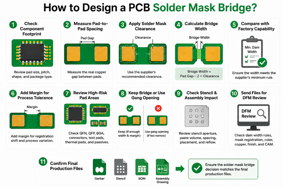
Step 1: Check the component footprint.
Review pad size, pad pitch, pad shape, and package type first. Fine-pitch QFN, QFP, BGA, connector, 0201, and 0402 areas need extra review because the remaining solder mask bridge is often very narrow.
Step 2: Measure the real pad-to-pad spacing.
Check the copper gap between adjacent pads, not only the component pitch. A 0.5 mm pitch part may still have a very small gap if the pads are wide. Pad gap is the starting value for bridge width calculation.
Step 3: Apply the correct solder mask clearance.
Use the PCB supplier’s recommended solder mask clearance instead of only using CAD defaults. Larger clearance exposes more copper but reduces the bridge. Smaller clearance protects the bridge but may cause solder mask to cover the pad edge.
Step 4: Calculate the solder mask bridge width.
Use this formula: bridge width = pad gap − 2 × solder mask clearance. For example, if the pad gap is 0.20 mm and clearance is 0.05 mm per side, the bridge width is 0.10 mm.
Step 5: Compare the result with factory capability.
Check whether the calculated width meets the supplier’s minimum solder mask dam rule. Also consider solder mask color, copper thickness, surface finish, and production quantity. A value that works for green solder mask may not work for black or white solder mask.
Step 6: Add margin for process tolerance.
Do not design exactly at the factory limit. Solder mask registration shift, exposure variation, developing pressure, and copper height can reduce the finished bridge. Add more margin for fine-pitch pads, heavy copper PCB, and matte solder mask.
Step 7: Review high-risk pad areas.
Check QFN side pads, QFP leads, BGA fanout, board-to-board connectors, test pad arrays, thermal pads, and small passive components. These areas often create missing dams, solder mask slivers, or bridge offset.
Step 8: Decide whether to keep the bridge or use gang opening.
Keep the bridge only when it has enough finished width and process margin. If it becomes a sliver or falls below the supplier’s limit, use a gang opening or adjust the pad design. A controlled gang opening is safer than an unstable narrow bridge.
Step 9: Check stencil and assembly impact.
If the bridge is removed, solder paste control becomes more important. Review stencil aperture size, paste volume, component spacing, placement accuracy, and reflow profile. This is especially important for fine-pitch ICs and QFN thermal pads.
Step 10: Send files for DFM review.
Ask the PCB supplier to check solder mask dam width rules, mask registration, solder mask color, copper thickness, surface finish, and CAM changes. Also confirm whether any solder mask openings will be enlarged during CAM processing.
Step 11: Confirm the final production files.
Before batch PCB or PCBA production, confirm whether the solder mask bridge is preserved, adjusted, or changed to gang opening. The approved Gerber, stencil file, BOM, and assembly drawing should match the final production decision.
FAQs About Solder Mask Bridge
Q1: Does a solder mask bridge improve PCBA yield?
A1: Yes. A stable bridge separates close pads and reduces solder bridging during reflow. It is useful for fine-pitch ICs, connectors, QFN pads, and small SMD parts. In batch PCBA, stable mask dams help reduce shorts and rework.
Q2: Can stencil design replace a solder mask bridge?
A2: Not fully. Stencil aperture reduction and paste volume control can reduce solder bridging, but they do not replace a physical mask barrier. Best results come from matching solder mask design, stencil design, and reflow control.
Q3: Is solder mask bridge width the same as pad spacing?
A3: No. Pad spacing is the copper gap. Bridge width is the mask left after clearance is applied. Bridge width = pad gap − 2 × solder mask clearance.
Q4: Why does the Gerber show a bridge but the PCB has no dam?
A4: The designed bridge may be below factory capability. It may be removed during CAM review or disappear during developing. A visible Gerber bridge does not guarantee a finished dam.
Q5: Do vias affect solder mask bridge design?
A5: Yes. Vias near pads can reduce mask space and create slivers. This is common near BGA fanout and dense test pads. Via tenting, plugging, and mask opening rules should be checked together.
Q6: Can solder mask bridge defects cause shorts?
A6: The mask itself is non-conductive, but missing dams, residue, burrs, or poor solder control can let solder connect nearby pads. The short usually comes from solder bridging, not from the mask material.
Q7: Should prototypes and mass production use the same bridge rule?
A7: Yes. A prototype may pass once with a narrow dam, but mass production needs repeatability. Use the final production rule before approving batch PCBA.
Q8: How should solder mask bridges be inspected before SMT?
A8: Check whether dams exist, whether they are centered, and whether there are missing dams, burrs, peeling, or residue.
Q9: Does solder mask thickness affect bridge reliability?
A9: Yes. Uneven or thin solder mask can weaken narrow dams. Heavy copper makes edge coverage harder.
Q10: Can thermal pads use solder mask bridges?
A10: Yes, but thermal pad areas need careful review. Large exposed pads may use segmented openings or stencil windowpane design.
Q11: What files should be sent for solder mask review?
A11: Send Gerber or ODB++, stackup, solder mask color, copper thickness, surface finish, BOM, and assembly requirements.
Q12: How can a PCBA supplier reduce solder bridging without dams?
A12: The supplier can reduce stencil apertures, control solder paste volume, improve placement accuracy, tune reflow, and inspect fine-pitch areas closely. When dams are removed, process control becomes more important.
Conclusion
A solder mask bridge affects solder control, short prevention, and PCBA yield. The bridge must be wide enough, centered, and stable after fabrication and assembly.
For reliable PCBA, review pad spacing, solder mask clearance, mask color, copper thickness, surface finish, stencil design, DFM results, and SMT process control before production.
EBest Circuit provides PCB fabrication, PCBA assembly, DFM review, stencil support, component sourcing, SMT assembly, testing, and batch production for global projects. Send your Gerber files, BOM, and assembly requirements to sales@bestpcbs.com for a fast PCB and PCBA quotation.